
CHAPTER EIGHT
Class A Amplifiers
8.1 INTRODUCTION
The class A amplifier is typically used as the first amplification stage of a receiver or a transmitter where minimum noise is desired. This is achieved with a cost of relatively low efficiency. In a receiver the first stage in an amplifier chain handles low power levels, so the low efficiency of the first amplifiers actually wastes little power. Power amplifiers with different class designations are used in later stages. The variety of amplifier classes are described in [1] and will be covered more extensively in Chapter 9. The primary properties of importance to class A amplifier design are gain, bandwidth control, stability, return loss, and noise figure. Noise figure was considered in Chapter 7, but the other topics are described in the present one.
8.2 DEFINITION OF GAIN [2]
In low-frequency circuits, gain is often thought of in terms of voltage or current gain, for example, the ratio of the output voltage across the load to the input applied voltage. At radio frequencies it is difficult to directly measure a voltage, so typically some form of gain is used. But once the notion of power is introduced, there are several definitions of power gain that might be used.
1. Power Gain This is the ratio of power dissipated in the load, ZL, to the power delivered to the input of the amplifier. This definition is independent of the generator impedance, ZG. Certain amplifiers, especially negative resistance amplifiers, are strongly dependent on ZG.
2. Available Gain This is the ratio of the amplifier output power to the available power from the generator source. This definition depends on ZG but is independent of ZL.
3. Exchangeable Gain This is the ratio of the output exchangeable power to the input exchangeable power. The exchangeable power of the source is defined as
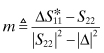
(8.1)
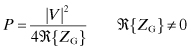
For negative resistance amplifiers P < 0! Furthermore, this definition is independent of ZL.
4. Insertion Gain This is the ratio of output power to the power that would be dissipated in the load if the amplifier were not present. There is a problem in applying this definition to mixers or parametric upconverters where the input and output frequencies differ.
5. Transducer Power Gain This is the ratio of the power delivered to the load to the available power from the source. This definition depends on both ZG and ZL. It gives positive gain for negative resistance amplifiers as well. Since the characteristics of real amplifiers change when either the load or generator impedance is changed, it is desirable that the gain definition reflect this characteristic. Thus, the transducer power gain definition is found to be the most useful.
8.3 TRANSDUCER POWER GAIN OF A TWO-PORT NETWORK
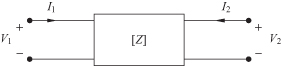
The linear two-port circuit in Fig. 8.1 is characterized by its impedance parameters:
(8.2)
![]()
FIGURE 8.1 Two-port circuit expressed in impedance parameters.
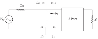
But the relationship between the port 2 voltage and current is determined by the load impedance as illustrated in Fig. 8.2:
FIGURE 8.2 Equivalent circuit to determine the input available power.
(8.4)
![]()
Substitution of this for V2 in Eq. (8.3) gives the input impedance. This is dependent on both the contents of the two-port circuit itself and also the load:
(8.5)
![]()
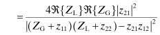
This will be used to determine the transducer power gain. The power delivered to the load is P2:
(8.6)
![]()
Since the power available from the source at port 1 is
(8.7)

the transducer power gain can be shown to be
(8.8)
![]()
(8.9)
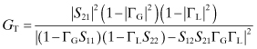
Similar expressions can be obtained for y, h, or g parameters by simply replacing the corresponding zij with the desired matrix elements and by replacing the ZG and ZL with the appropriate termination. However, for RF and microwave circuits, scattering parameters are the most readily measured quantities. The transducer power gain will be found in terms of the scattering parameters in the following section.
8.4 TRANSDUCER POWER GAIN USING S PARAMETERS
The available power, Pa, when the input of the two-port circuit is matched with ![]() , was given by Eq. (4.170) in Chapter
4:
, was given by Eq. (4.170) in Chapter
4:

At the output side of the circuit, the power delivered to the load is given by the following:
The transducer gain is simply the ratio of Eq. (8.11) to Eq. (8.10):
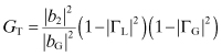
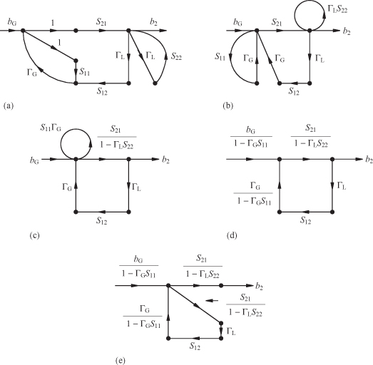
As this stands, b2 and bG are not very meaningful. However, this ratio can be expressed entirely in terms of the known S parameters of the two-port circuit. From the description of the S parameters as a matrix corresponding to forward- and backward-traveling waves, the two-port circuit can be represented in terms of a flow graph. Each branch of the flow graph is unidirectional and the combination describes the S matrix completely. The presumption is that the circuit is linear. The problem of finding b2/bG can be done using either algebra or some flow graph reduction technique. The classical method developed for linear systems represented as flow graphs uses Mason’s nontouching loop rules. The method shown below is easier to remember, but it is more complicated to administer to complex circuits that require a computer analysis. For the relatively simple graph shown in Fig. 8.3 the simpler method works well. This method of flow graph reduction is based on four rules:
1. The cascade of two branches in series can be reduced to one branch with the value equal to the product of the two original branches (Fig. 8.4a).
2. Two parallel branches can be reduced to one branch whose value is the sum of the two original branches (Fig. 8.4b).
3. As illustrated in Fig. 8.4c, a self-loop with value Y with an incoming branch X can be reduced to a single line of value
(8.13)
![]()
4. The transfer function remains unchanged if a node with one input branch and N output branches can be split into two nodes. The input branch goes to each of the new nodes. Similarly, the transfer function remains unchanged if a node with one output branch and N input branches can be split into two nodes. The output branch goes to each of the new nodes (Fig. 8.4d).
FIGURE 8.3 Flow graph equivalent of two-port circuit in Fig. 8.2.
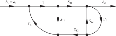
FIGURE 8.4 Flow graph reduction rules for (a) two series branches, (b) two shunt branches, (c) a self-loop, and (d) splitting a node.
These rules can be used to finish the calculation of the transducer power gain of expression (8.12) by finding b2/bG. The first step in this reduction is the splitting of two nodes shown in Fig 8.5a by use of rule 4. This forms a self-loop in the right-hand side of the circuit. The lower left-hand node is also split into two nodes (Fig. 8.5b). The incoming branches to the self-loop on the right-hand side are modified by means of rule 3 (Fig. 8.5c). In the same figure, another self-loop is made evident on the left-hand side. In this case there are two incoming branches modified by the self-loop. Use of rule 3 produces Fig. 8.5d. Splitting the node by means of rule 4 results in Fig. 8.5e. The resulting self-loop modifies the incoming branch on the left-hand side (rule 3). The result is three branches in series (rule 1) so the transfer function can now be written by inspection:
(8.14)
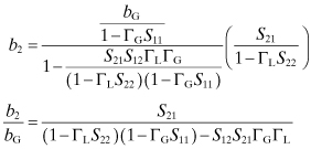
FIGURE 8.5 Demonstration of amplifier flow graph.
This ratio can be substituted into the transducer power gain expression Eq. (8.12). Thus, the transducer power gain is known in terms of the scattering parameters of the two-port circuit and the terminating reflection coefficients:
(8.15)

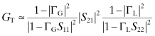
This is the full equation for the transducer power gain. Other
expressions making use of approximations are strictly speaking a fiction, though
this fiction is sometimes used to characterize certain transistors. For example,
unilateral power gain is found by setting S12
= 0. In real transistors S12 should be small,
but it is never actually 0. The maximum unilateral power gain is found by setting
S12 = 0, ![]() , and
, and ![]() :
:
(8.16)
8.5 SIMULTANEOUS MATCH FOR MAXIMUM POWER GAIN
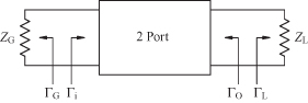
Maximum gain is obtained when both the input and output ports are simultaneously matched. One way to achieve this is to guess at a ΓL and calculate Γi (Fig. 8.6). The generator impedance then is made to match the complex conjugate of Γi. With this new value of ΓG, a new value of Γo is found. Matching this to ΓL means the that ΓL changes. This iterative process continues until both sides of the circuit are simultaneously matched.
FIGURE 8.6 Definition of reflection coefficients for two-port circuit.
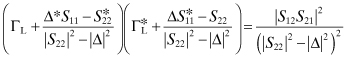
A better way is to recognize this as basically a problem with two equations and two unknowns. Simultaneous match forces the following two requirements:
Since both of these equations have to be satisfied simultaneously, finding ΓG and ΓL requires solution of two equations with two unknowns. These can be written in terms of the determinate of the S matrix, Δ, as follows:.
Substitution of Eq. (8.20) into Eq. (8.19) eliminates ΓL:
(8.21)
This expression can be rearranged in the usual quadratic form. After taking the complex conjugate, this yields the following:
(8.22)
![]()
This equation can be rewritten in the form
where
(8.24)
![]()
(8.25)
![]()
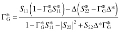
In the solution of Eq. (8.23) the required generator reflection coefficient for maximum gain is
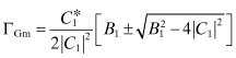
In a similar fashion the load reflection coefficient for maximum gain is
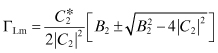
where
(8.28)
![]()
(8.29)
![]()
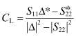
The parameters Bi and Ci are determined solely from the scattering parameters of the two-port circuit. The − sign is used when Bi > 0, and the + sign is used when Bi < 0. Once the terminating reflection coefficients are known, the corresponding impedances may be determined:
(8.30)
![]()
(8.31)
![]()
8.6 STABILITY
A stable amplifier is an amplifier where there are no unwanted oscillations anywhere. Instability outside the operating band of the amplifier can still cause unwanted noise and even device burn out. Oscillations can only occur when there is some feedback path from the output back to the input. This feedback can be a result of an external circuit, external feedback parasitic circuit elements, or by an internal feedback path such as through Cμ in a common emitter bipolar transistor. Of these three sources, the last is usually the most troublesome. The following sections describe a method for determining transistor stability and some procedures to stabilize an otherwise unstable transistor.
8.6.1 Stability Circles
The criteria for unconditional stability require that
|Γi| ≤ 1 and |Γo| ≤ 1 for any passive terminating loads. A
useful amplifier may still be made if the terminating loads are carefully chosen to
stay out of the unstable regions. It is helpful to find the borderline between the
stable and the unstable regions. For the input side, this is done by finding the
locus of points of ΓL that will give |Γi| = 1. The borderline
between stability and instability is found from Eq. (8.19) when ![]() and |Γi| = 1:
and |Γi| = 1:
(8.32)
![]()
This can be squared and then split up into its complex conjugate pairs:
(8.33)
![]()
The coefficients of the different forms of ΓL are collected together:
(8.34)
![]()
Equation (8.35) can be put in a form that can be factored by completing the square. The value |m|2, defined below, is added to both sides of this equation:

where
Substitution of Eq. (8.37) into Eq. (8.36) and upon simplification yields the following factored form:
This is the equation of a circle whose center is
The radius of the load stability circle is
The center and radius for the generator stability circle can be found by symmetry:
(8.41)
(8.42)
These two circles, one for the load and one for the generator, represent the borderline between stability and instability. These two circles can be overlaid on a Smith chart. The center of the circle is located at the vectorial position relative to the center of the Smith chart. The “dimensions” for the center and radius are normalized to the Smith chart radius (whose value is unity).
The remaining issue is which side of these circles is the stable region.
Consider first the load stability circle shown in Fig. 8.7. If a matched transmission line with Z0 = 50 ![]() were
connected directly to the output port of the two-port circuit, then ΓL =
0. This load would be located in the center of the Smith chart. Under this
condition, Eq. (8.17) indicates that
Γi = S11. If the known value
of |S11| < 1, then |Γi|
< 1 when the load is at the center of the Smith chart. If one point on one
side of the stability circle is known to be stable, then all points on that side of
the stability circle are also stable. The same rule would apply to the load side
when ZG is replaced by a matched load =Z0. Then from Eq. (8.18) Γo = S22.
were
connected directly to the output port of the two-port circuit, then ΓL =
0. This load would be located in the center of the Smith chart. Under this
condition, Eq. (8.17) indicates that
Γi = S11. If the known value
of |S11| < 1, then |Γi|
< 1 when the load is at the center of the Smith chart. If one point on one
side of the stability circle is known to be stable, then all points on that side of
the stability circle are also stable. The same rule would apply to the load side
when ZG is replaced by a matched load =Z0. Then from Eq. (8.18) Γo = S22.
FIGURE 8.7 Illustration of stability circles where shaded region is unstable.
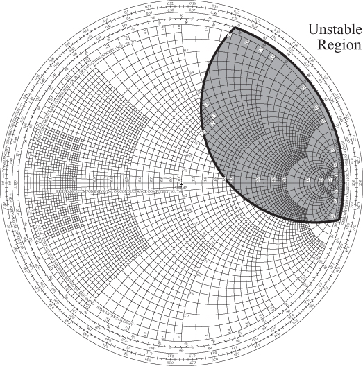
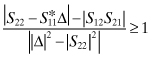
Unconditional stability requires that both |Γi| < 1 and |Γo| < 1 for any passive load and generator impedances attached to the ports. In this case if |S11| < 1 and |S22| < 1, the stability circles would lie completely outside the Smith chart. Conditional stability occurs when at least one of the stability circles intersects the Smith chart. As long as the load and source impedances are on the stable side of the stability circle, stable operation occurs. Avoiding unstable regions for a potentially unstable transistor will usually not provide the maximum transducer power gain condition as given by Eqs. (8.26) and (8.27). Avoiding unstable operation will usually require compromising the maximum gain for a slightly smaller but often acceptable gain. Clearly, using an impedance too close to the edge of the stability circle can result in unstable operation because of manufacturing tolerances. It is usually best to have an unconditionally stable circuit. An approach to make this happen is given in Section 8.6.3.
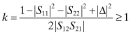
8.6.2 Rollett Criteria for Unconditional Stability
It is often useful to determine if a given transistor is unconditionally stable for any pair of passive impedances terminating the transistor. The two conditions necessary for this are known as the Rollett stability criteria [3] and are given as follows:
Rollett’s original derivation was done using any one of the volt-ampere immittance parameters, z, y, h, or g. Subsequently, Rollett’s stability equations were expressed in terms of S parameters as shown in Eqs. (8.43) and (8.44). Others arrived at stability conditions that appeared different from these, but it was pointed out that most of these alternate formulations were equivalent to those in Eqs. (8.43) and (8.44) [4]. The derivation of these two quantities will be given in this section.
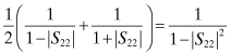
The first of these equations is based on unconditional stability occurring when the load stability circle lies completely outside the Smith chart and when |S11| < 1, that is,
or
where Eq. (8.46) describes the case where the stability circle encompasses the entire Smith chart within it. Substitution of Eqs. (8.39) and (8.40) into Eq. (8.45) gives
Squaring Eq. (8.47) gives the following:
(8.48)
![]()
(8.49)
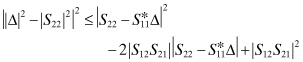
The last term on the right-hand side of Eq. (8.50) can be expanded:
(8.51)
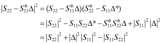
Expansion of |Δ|2 gives
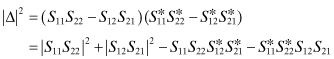
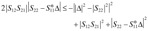
By subtracting |S12S21|2 inside the parenthesis in Eq. (8.52) and adding the same value outside the parenthesis, the quantity inside the parenthesis is equivalent to |Δ|2 given in Eq. (8.53). Thus Eq. (8.52) can be factored as shown below:
(8.54)
where Eq. (8.55) is based on the temporary definitions:
(8.56)
![]()
(8.57)
![]()
(8.58)
![]()
The original inequality, Eq. (8.50), written in terms of these new variables is
By first squaring both sides and then canceling terms, Eq. (8.59) can be greatly simplified:
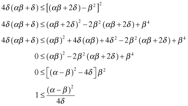
Taking the square root of Eq. (8.60) yields
(8.61)
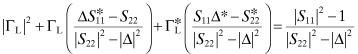
This is the same as Eq. (8.43), which has now been demonstrated. Since the value of k is symmetrical on interchange of ports 1 and 2, the same result would occur with either the generator or load port stability circle.
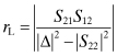
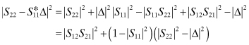
The second condition for unconditional stability, Eq. (8.44), can also be demonstrated based on the requirement that |Γi| < 1. The second term of the right-hand side of Eq. (8.17) can be modified by multiplying it by 1 (=S22/S22) and adding 0 (=S12S21 − S12S21) to the numerator. This results in the following:

The complex quantity 1 − ΓLS22 can be written in polar form as 1 − |ΓLS22|ejθ. Any passive load must lie within the unit circle |ΓL| ≤ 1, so |ΓL| is set to 1. As described in [5], the quantity
![]()
which appears in Eq. (8.62), is a circle as pictured in Fig. 8.8 centered at
and with radius
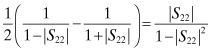
FIGURE 8.8 Representation of circle with |ΓL| = 1.

Equation (8.62) is expressed in terms of this circle:
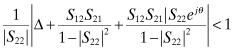
The phase of the load is chosen so that it maximizes the left-hand side of Eq. (8.63). However, it must still obey the stated inequality. This means that Eq. (8.63) can be written as the sum of the two magnitudes without violating the inequality condition:
Comparison of the far right-hand side of this expression with 0 results in the following inequality:
If the process had begun with the condition that |Γo| < 1, then the result would be the same as Eq. (8.64) with the 1’s and 2’s interchanged:
When Eqs. (8.64) and (8.65) are added together,
However, from the definition of the determinate of the S parameter matrix,
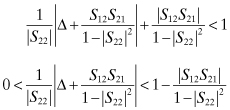
When the term |S12S21| in Eq. (8.67) is replaced with something larger, as given in Eq. (8.66), the inequality is still true:
(8.68)
An alternate, but equivalent, set of requirements for stability are [4]
(8.69)
![]()
and either
or
The requirement of Eq. (8.70a) or (8.70b) is equivalent to |Δ| < 1.
8.6.3 Stabilizing a Transistor Amplifier
There are a variety of approaches to stabilizing an amplifier. In Section 8.6.1, it was suggested that stability could be achieved from a potentially unstable transistor by making sure the chosen amplifier terminating impedances remain inside the stable regions at all frequencies as determined by the stability circles.
Another method would be to load the amplifier with an additional shunt or series resistor on either the generator or load side. The resistor is incorporated as part of the the two-port parameters of the transistor. If the condition for unconditional stability is achieved for this expanded transistor model, then optimization can be performed for the other circuit elements in order to achieve the desired gain and bandwidth. It is usually better to try loading the output side rather than the input side in order to minimize increasing the amplifier noise figure.
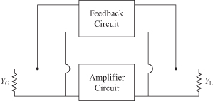
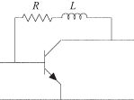
Another approach that is sometimes useful is to introduce an external feedback path that can neutralize the internal feedback of the transistor. The most widely used scheme is the shunt–shunt feedback circuit shown in Fig. 8.9. The y parameters for the composite circuit are simply the sum of the y parameters of the amplifier and feedback two-port circuits:
(8.71)
![]()
FIGURE 8.9 Shunt–shunt feedback for stabilizing a transistor.
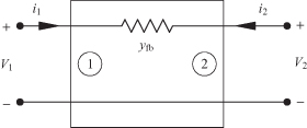
To use this method, the transistor scattering parameters must be converted to admittance parameters (Appendix D). The y parameters for a simple series admittance, yfb can be found from circuit theory (Fig. 8.10):
(8.72)
![]()
(8.73)
![]()
FIGURE 8.10 Two-port representation of feedback circuit.
Consequently, the composite y parameters are
(8.74)
![]()
(8.75)
![]()
(8.76)
![]()
(8.77)
![]()
If y12c could be made to be zero, then S12c would also be zero and unconditional stability could be achieved:
(8.78)
![]()
Since the circuit parameter g12a < 0 the value gfb < 0 must be true also. Since it is not possible to have a negative passive conductance, complete removal of the internal feedback is not possible. However, the susceptance, b12a can be canceled by a passive external feedback susceptance. Although total removal of y12a cannot be achieved, yet progress toward stabilizing the amplifier can often be achieved. There is no guarantee that neutralization will provide a composite y matrix that is unconditionally stable. In addition, neutralization of the feedback susceptance occurs at only one frequency.
As an example, consider a transistor to have the following S parameters at a given frequency:
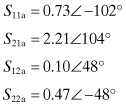
For this transistor, k = 0.752 and |Δ| = 0.294 as found from Eqs. (8.43) and (8.44). Conversion of the S parameters given by Eq. (8.79) to y parameters gives
(8.80)
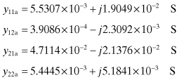
Nothing can be done about g12a, but b12a can be removed by setting bfb = b12a = −2.3092 × 10⁻³. The composite admittance matrix becomes
(8.81)
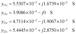
The composite scattering parameters can now be found and the stability factor calculated yielding k = 2.067 and |Δ| = 0.4037. The transistor with the feedback circuit is unconditionally stable at the given frequency. This stability has been achieved by adding inductive susceptance in shunt with the transistor input and output ports.
Broadband stability can be achieved by replacing the feedback inductor with an inductor and resistor as shown in Fig. 8.11. A starting value for the inductor can be found as described for the single-frequency analysis. The resistor is typically in the 200- to 800-Ω range, but optimum values for R and L are best found by computer optimization.
FIGURE 8.11 Broadband feedback stabilization.
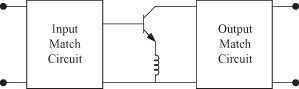
8.7 CLASS A POWER AMPLIFIERS
Class A amplifiers, whether for small-signal or large-signal operation, are intended to amplify the incoming signal in a linear fashion. This type of amplifier will not introduce significant distortion in the amplitude and phase of the signal. A linear class A power amplifier will introduce low-amplitude harmonic frequency components and low intermodulation distortion (IMD). An example of IMD can be described in terms of a double sideband suppressed carrier wave that is represented as
(8.82)
![]()
where ωc is the high-frequency carrier frequency and ωm is the low-frequency modulation frequency. Intermodulation distortion would result in frequencies at ωc ± nωm and harmonic distortion would cause frequency generation at kωc ± nωm. The later harmonic distortion can usually be filtered out, but the third-order IMD is more difficult to handle because the distortion frequencies are near if not actually inside the system pass band. Clearly, this distortion in a class A amplifier is a greater problem for power amplifiers than for small-signal amplifiers. Reduction of IMD depends on efficient power combining methods and careful design of the transistors themselves.
A transistor acting in the class A mode remains in its active state throughout the complete cycle of the signal. Two examples of common emitter class A amplifiers are shown in Fig. 8.12. The maximum efficiency of the class A amplifier in Fig. 8.12a has been shown to be 25% (e.g., see [6]). However, if an RF coil can be used in the collector (Fig. 8.12b), the efficiency can be increased to almost 50%. This can be shown by recognizing first that there is no ac flow in the bias source and no dc flow in the load, RL. The total current flowing in the transistor collector is
(8.83)
![]()
and the total collector voltage is
(8.84)
![]()
FIGURE 8.12 Class A amplifiers with (a) collector resistor and (b) collector inductor.
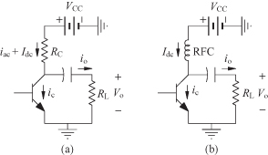
Both the quiescent current, IQ, and the output current, Io, are defined in Fig. 8.13. The quiescent current, IQ, is the direct current flowing through the collector, which sets the ac operating point. When the load is drawing the maximum instantaneous power,
(8.85)
![]()
FIGURE 8.13 Magnitude of output current and quiescent current of class A amplifier.
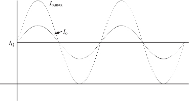
At this point, the maximum output voltage is
(8.86)
![]()
where |Vo,max| ≈ VCC.
The dc power source supplies
(8.87)
![]()
The maximum average power delivered to the load can now be written in terms of the supply voltage:
(8.88)
![]()
The collector efficiency is
(8.89)
![]()
This definition is meaningful for high-gain amplifiers where Pi
![]() Po. For the class A amplifier the maximum
collector efficiency is ηc ≈ 50%. The Vo,max will always be slightly less than the
supply voltage because of Vbe or Vce,sat. However, it should be noted that many
times high-power amplifiers do not have high gain, so the power-added efficiency
offers a more useful quality factor for a transistor than if Pi were neglected. Power-added efficiency will be used in
Section 8.9.2 for analysis of multistage amplifiers.
Po. For the class A amplifier the maximum
collector efficiency is ηc ≈ 50%. The Vo,max will always be slightly less than the
supply voltage because of Vbe or Vce,sat. However, it should be noted that many
times high-power amplifiers do not have high gain, so the power-added efficiency
offers a more useful quality factor for a transistor than if Pi were neglected. Power-added efficiency will be used in
Section 8.9.2 for analysis of multistage amplifiers.
8.8 POWER COMBINING OF POWER AMPLIFIERS
Design of power FET amplifiers requires use of large-gate
periphery devices. However, eventually, the large gate periphery causes other
problems, such as impedance matching especially at RF and microwave frequencies.
Bandwidth improvement can be obtained by combining several transistors, often on a
single chip. An example of combining two transistors is shown in Fig. 8.14 [7, 8]. The separation of the
transistors may induce odd-order oscillations in the circuit even if the stability
factor of the individual transistors (even-order stability) indicate they are
stable. This odd-order instability can be controlled by adding Rodd between the two drains to damp out such oscillations.
This resistor is typically less than 400 ![]() .
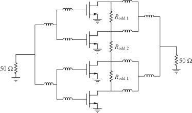
Symmetry indicates no power dissipation when the outputs of the two transistors are
equal and in phase. An example of a four-transistor combining circuit is shown in
Fig. 8.15, which now includes resistors
Rodd1 and Rodd2 to help suppress odd-order oscillations.
.
Symmetry indicates no power dissipation when the outputs of the two transistors are
equal and in phase. An example of a four-transistor combining circuit is shown in
Fig. 8.15, which now includes resistors
Rodd1 and Rodd2 to help suppress odd-order oscillations.
FIGURE 8.14 Power combining two transistors [7, 8].
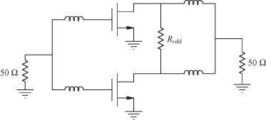
FIGURE 8.15 Power combining four transistors [7, 8].
8.9 PROPERTIES OF CASCADED AMPLIFIERS
An ideal amplifier is completely unilateral so that there is no feedback signal returning from the output to the input side. Under this condition, analysis of cascaded amplifiers results in some interesting properties related to noise figure and efficiency. The results obtained will be approximately valid for almost unilateral amplifiers, even if some of the “amplifiers” are mixers or attenuators. The following two sections deal with the total noise figure and total efficiency, respectively, of a cascade of unilateral amplifiers.
8.9.1 Friis Noise Formula
The most critical part for achieving low noise in a receiver is the noise figure and gain of the first stage. This is intuitively clear since the magnitude of the noise in the first stage will be a much larger percentage of the incoming signal than it will be in subsequent stages where the signal amplitude is much larger. Although both signal and noise get amplified the same amount, the difference between the signal and noise increases. For a receiver with n unilateral stages, the total noise factor for all n stages is [9]
where NT,n is the total noise power delivered to the load. This can be expressed in terms of the sum of the noise added by the last stage, Nn, and that of all the previous stages multiplied by the gain of the last stage:
If the nth stage were removed, and its noise factor measured alone, then its noise factor would be
(8.92)
![]()
By substitution Eq. (8.91) into Eq. (8.90) an expression for the noise factor is obtained that separates the contributions of the noise coming from the last stage only from the previous n − 1 stages:
(8.94)
![]()
Canceling the Gn in the second term and substituting (8.93) yields
The second term in Eq. (8.95) is the same as Eq. (8.90) except that n has been reduced to n − 1. This process is repeated n times, giving what is known as the Friis formula for the noise factor for a cascade of unilateral gain stages:
(8.96)
![]()
Clearly, the noise factor of the first stage is the most important contributor to the overall noise factor of the system. If the first stage has reasonable gain, the subsequent stages can have much higher noise factor without affecting the overall noise factor of the receiver.
8.9.2 Multistage Amplifier Efficiency
For a multistage amplifier, the overall power efficiency can be found that will correspond in some way with the overall noise figure expression. Unlike the noise figure, however, the efficiency of the last stage will be found to be most important. Again, this would appear logical since the last amplifying stage handles the greatest amount of power so that poor efficiency here would waste the most amount of power. For the kth stage of an n-stage amplifier chain, the power-added efficiency is
where
| P o, k = output power of the kth stage |
| P i, k = input power to the kth stage |
| P d, k = source of power, which is typically the dc bias for the kth stage |
If the input power to the first stage is Pi,1, then
and for the kth stage alone
When Eqs. (8.98) and (8.99) are substituted into the efficiency equation, Eq. (8.97), the power from the power source can be found:
(8.100)
![]()
The total added power for a chain of n amplifiers is
(8.101)
![]()
The efficiency for the whole amplifier chain is clearly given by the following:

Replacing the power levels in Eq. (8.102) with their explicit expression gives the value for the overall efficiency of a chain of unilateral amplifiers:
(8.103)
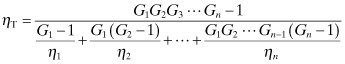
When each amplifier stage has a gain sufficiently greater than 1, the overall efficiency becomes
(8.104)
This final equation highlights the assertion that it is most important to make the final stage the most efficient one.
8.10 AMPLIFIER DESIGN FOR OPTIMUM GAIN AND NOISE
The gain for a nonunilateral amplifier was previously given as Eq. (8.18) is repeated here:
(8.105)
If S12 is set to zero, thereby invoking the unilateral approximation for the amplifier gain, then
(8.106)
This approximation, of course, removes the possibility of analytically determining the transistor stability conditions. Using this expression, a set of constant gain circles can be drawn on a Smith chart for a given transistor. That is, for a given set of device scattering parameters and for a fixed load impedance, a set of constant gain circles can be drawn for a range of generator impedances expressed here in terms of ΓG.
The noise figure was previously found in Eq. (7.40). As was done for the
constant gain circles, constant noise figure circles can be drawn for a range of
values for the generator admittance, YG =
GG + jBG. The optimum gain occurs when ![]() and the minimum noise figure occurs
when YG = Yopt. These two source impedances are rarely the same, but a
procedure is available to at least optimize for both of these parameters
simultaneously [10]. As seen on the Smith chart in Fig. 8.16, it appears possible that the least damage to
either the gain or the noise figure is obtained if the actual chosen generator
impedance lies on a line between
and the minimum noise figure occurs
when YG = Yopt. These two source impedances are rarely the same, but a
procedure is available to at least optimize for both of these parameters
simultaneously [10]. As seen on the Smith chart in Fig. 8.16, it appears possible that the least damage to
either the gain or the noise figure is obtained if the actual chosen generator
impedance lies on a line between ![]() and
Yopt. It has been found that addition of
series emitter inductance, such as shown in Fig. 8.17, will lower the minimum noise figure of the circuit
because it lowers the effective Fmin and
rn. This series inductance also increases
the real part of the input impedance. The output impedance does not affect the noise
figure but can be manipulated to adjust the gain.
and
Yopt. It has been found that addition of
series emitter inductance, such as shown in Fig. 8.17, will lower the minimum noise figure of the circuit
because it lowers the effective Fmin and
rn. This series inductance also increases
the real part of the input impedance. The output impedance does not affect the noise
figure but can be manipulated to adjust the gain.
FIGURE 8.16 Constant gain and noise figure circles.
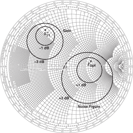
FIGURE 8.17 Series inductive feedback can be used to lower noise figure.
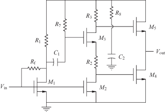
Low-noise, wide-band amplifiers have been reported using CMOS technology. Wide bandwidth can be achieved using negative feedback by using a resistor between the gate and source (or base and emitter). Since the gain is reduce by the factor of 1 + T where T is the loop gain, then the bandwidth increases by 1 + T. However, even a larger bandwidth and a better noise figure can be achieved by using inductive source (or emitter) degeneracy along with an added input inductor and shunt capacitor [11]. Inductors are problematic in integrated circuit (IC) designs because of their size and relatively poor Q. A wide-bandwidth CMOS circuit with a noise figure below 4.8 dB has been reported that uses no inductors. Low noise is achieved in Fig. 8.18 by using a feed-forward technique that effectively cancels noise [12]. This circuit provides not only noise cancellation but enhanced gain (11 dB in this case) that former feed-forward designs lacked. Noise coming out of the input matching transistor, M1, is canceled by M2 and M3, and delivered to M4 and M5 through two feed-forward paths. The capacitor C2 is large enough to provide an effective RF ground.
FIGURE 8.18 Feed-forward noise cancellation low-noise amplifier described in [12].
8.11 CONCLUSION
This chapter began with a definition and graphical derivation of the most useful form of power gain, the transducer power gain. A linear analysis of an amplifier focuses on gain, bandwidth, stability, and noise. An analytical treatment for bandwidth is usually intractable, so this aspect is normally done by computer simulation. An introduction to class A power amplifiers is given along with a schematic of at least one integrated circuit low-noise amplifier that can be implemented with CMOS technology.
PROBLEMS
8.1. Using the flow graph reduction method, verify the reflection coefficient found in Eq. (8.17).
8.2. The measured scattering parameters of a transistor in an amplifier circuit are found to be the following:
a. Determine the stability factor, k, for this transistor.
b. Determine the y parameters for this circuit.
c. Determine the circuit at 1.5 GHz that would neutralize (almost unilateralize) the circuit. While this procedure does not guarantee stability in all cases, it usually helps lead toward greater stability.
d. Determine the new scattering parameters for the neutralized circuit.
e. Determine the generator and load impedances that would give maximum transducer power gain (not unilateral power gain).
f. What is the value for the maximum transducer power gain?
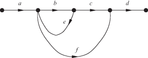
8.3. Determine the transfer function for the flow graph in Fig. 8.19.
FIGURE 8.19 Flow graph for Problem 8.3.
8.4. A certain transistor has the following S parameters:
![]()
Determine whether this transistor is unconditionally stable.
8.5. Verify Eq. (8.38).
8.6. A three-stage amplifier consists of three individual unilateral amplifiers. The first one (the input stage) has a gain G1 = 10 dB, a noise factor F1 = 1.5, and an efficiency η1 = 1%. For stage 2, G2 = 20 dB, F2 = 10, and η2 = 5%. For stage 3, G3 = 5 dB, F3 = 15, and η3 = 50%. What is the overall total noise factor for the cascaded amplifier? What is the overall total efficiency for the cascaded amplifier?
REFERENCES
1. H. L. Krauss, C. W. Bostian, and F. H. Raab, Solid State Radio Engineering, New York: Wiley, pp. 371–382, 1980.
2. P. J. Khan, private communication, 1971.
3. J. M. Rollett, “Stability and Power-Gain Invariants of Linear Twoports,” IRE Trans. Circuit Theory, CT-9, pp. 29–32, March 1962.
4. D. Woods, “Reappraisal of the Unconditional Stability Criteria for Active 2-Port Networks in Terms of S Parameters” IEEE Trans. Circuits Syst., CAS-23, pp. 73–81, Feb. 1976.
5. T. T. Ha, Solid State Microwave Amplifier Design, New York: Wiley, 1981.
6. S. G. Burns and P. R. Bond, Principles of Electronic Circuits, Boston: PWS Publishing, 1997.
7. R. G. Reitag, S. H. Lee, and D. M. Krafcsik, “Stability and Improved Circuit Modeling Considerations for High Power MMIC Amplifiers,” 1988 IEEE Microwave Theory Tech. Symp. Digest, pp. 175–178, 1988.
8. R. G. Freitag “A Unified Analysis of MMIC Power Amplifier Stability,” 1992 IEEE Microwave Theory Tech. Symp. Digest, pp. 297–300, 1992.
9. H. T. Friis, “Noise Figures of Radio Receivers,” Proc. IRE, 32, pp. 419–422, July 1944.
10. R. E. Lehmann and D. D. Heston, “X-Band Monolithic Series Feedback LNA,” IEEE Trans. Microwave Theory Tech., MTT-33, pp. 1560–1566, Dec. 1985.
11. A. Bevilacqua and A. M. Niknejad, “An Ultrawideband CMOS Low-Noise Amplifier for 3.1–10.6-GHz Wireless Receivers,” IEEE J. Solid State Circuits, 39, pp. 2259–2268, Dec. 2004.
12. Q. Li and Y. P. Zhang, “A 1.5-V 2–9.6-GHz Inductorless Low-Noise Amplifier in 0.13-µm CMOS,” IEEE Trans. Microwave Theory Tech., 55, Oct. 2007.