
CHAPTER TWELVE
Phase-Lock Loops
12.1 INTRODUCTION
Phase-lock loops (PLL) became widespread with the availability of high-quality integrated circuit operational amplifiers (op-amps) in the 1960s. Since then this versatile circuit has found applications across the frequency spectrum in consumer, commercial, deep space, and military projects. Understanding the operation of the PLL incorporates RF techniques, oscillator design, closed-loop control theory, analog circuit design, and digital circuit design. The references listed at the end of this chapter provide insight beyond the present scope [1–4]. This chapter begins with the basic concepts, which are later expanded into practical designs.
12.2 PLL DESIGN BACKGROUND
The PLL uses negative feedback to tailor its performance. The primary design parameters are response time, transient performances, bandwidth, damping ratio, and phase margin. The type and order of a closed-loop system define the complexity and response to a stimulus. At least two of the components of a PLL, the voltage-controlled oscillator (VCO) and the phase detector, are high-frequency components. There may also be amplifiers, mixers, frequency multipliers, and other oscillators that require RF techniques.
Many integrated circuits are presently available that combine many of the PLL functions on a single chip. Operational amplifiers often are used in filter circuits, which may be either inverting or noninverting designs as required by the phase-lock loop design. Integrators, dc amplifiers, Schmitt triggers, and offset circuits are used to set the loop operation. Resistor/capacitor circuits provide phase shift for stability. The VCO keeps the loop locked.
12.3 PLL APPLICATIONS
A phase-lock loop can be used to multiply, divide, or filter different frequencies. The latter is illustrated in a space probe rapidly moving away from Earth. To recover data from the probe, the transmitter frequency must be known. The signal is very weak because of the distance, and the low signal-to-noise ratio requires a very small receiver filter bandwidth to recover the data. However, because of the relative motion, there is a significant and changing Doppler shift to the transmit frequency. The system requires a filter that may be only a few hertz wide, operating at a varying frequency that is centered at several gigahertz. The PLL helps keep the filter centered on the correct frequency.
An electronic PLL is one form of a closed-loop system. The cruise control in an automobile is another. A switching power supply, a camera’s light meter, a radio’s automatic gain control, the temperature control in a building, a car’s emission system controls, and a touch-tone dialing system are examples of closed-loop systems. A broadcast receiver changes frequency with a button push or electronically. Each time the station is accurately centered with no manual adjustment required. Physically, these PLLs are all very different, but they all have common characteristics and must be made stable.
The concept of feedback control is illustrated by the simple action of controlling the speed of a car. If the desired speed is 60 mph, then this becomes the reference speed. Any deviation from this speed is an error. The accelerator pedal is the control element. On level terrain, a constant pressure on the pedal will maintain constant speed. As the car goes up a hill, it will slow down, and the difference between the actual speed and the reference value generates an error. This error generates a command to push the accelerator pedal to increase the speed, but there will continue to be a slight error. As the car crests the hill and starts down, the speed will increase. Releasing pedal pressure will slow the acceleration, but an error will remain until a steady-state condition is again reached. For this example, the driver’s brain is the feedback path. The driver controls the sense of the feedback by knowing when to push and when to release the pedal. By his reaction time, he controls how close to the reference he maintains the car’s speed. He may decide to rapidly change the correction to tightly match the desired speed, or he may choose to compensate slowly so his speed averages out to the correct value. His actions coupled with the car’s controls form a system closely analogous to a phase-lock loop. Replace the human with an electrical circuit that senses the speed error, include another circuit that tempers the response time, and couple it to the accelerator controls. This is the typical cruise control system.
12.4 PLL BASICS
A PLL is a closed-loop system used for frequency control. Three and sometimes four building blocks are common to most PLL designs:
1. The phase detector.
2. The loop filter.
3. The voltage-controlled oscillator.
4. In addition a frequency divider is used when the output frequency is to be a multiple of the reference input frequency.
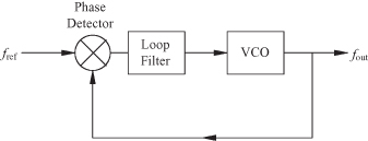
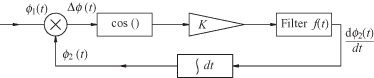
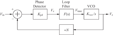
Figure 12.1 illustrates the connection of these blocks to make a complete phase-lock loop. The phase detector has two inputs and one output. This block can be realized by a specialized mixer based on those described in Chapter 11 where the IF port pass band goes down to dc. If the two input signals are very close in frequency, then the output will contain a term at twice the input frequency and a term that is almost zero frequency. The loop error signal in the PLL is the near-zero term. This error signal goes to the loop filter, which may be as simple as a capacitor and a resistor, or it can be one or more operational amplifiers with many resistors and capacitors. The VCO is the control element of this loop. The input is a control voltage from the loop filter, while the output is the required frequency. The time integral of this frequency is the phase that when compared with the input phase gives the error voltage to the loop filter.
FIGURE 12.1 Basic phase-lock loop.
When the loop is first turned on, the VCO frequency is not controlled by an error voltage. The loop filter output voltage can be anywhere between the high and low limits set by the power supply. However, the phase detector produces an error voltage that is the difference between the actual VCO frequency and the reference frequency. Like the cruise control example, this signal tells the loop filter whether the VCO frequency is too high or too low relative to the reference frequency. If the error signal indicates that the VCO frequency is less than the reference, the loop filter adjusts the control voltage to raise the VCO frequency. If the VCO frequency is too high, the loop filter changes the voltage and lowers the VCO frequency. The loop filter sets how fast the error is corrected. Some loops may be designed for a fast bumpy ride, while others may require a slow response, resulting in a smooth ride. When the loop filter has done its job, the VCO frequency will exactly match the reference frequency, and the two inputs will have a constant phase difference. This match in frequency and constant phase difference will be maintained even if the reference frequency changes. With each change, the PLL again goes through the settling out process. If the reference is noisy, the PLL is in a continual state of change, working hard to follow the input.
12.5 LOOP DESIGN PRINCIPLES
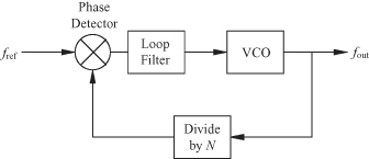
The important top-level PLL parameters are the input and output frequency, the response time, the loop bandwidth, and the loop damping ratio. The PLL block diagram in Fig. 12.2 includes a frequency divider in the feedback path. Both frequencies coming into the phase detector must be locked together at the same frequency. This will force the output frequency, fout, to be N times the reference frequency, fref. The actual design process can be summarized in three steps. First, each component should be thoroughly understood and tested individually. Second, when the components are assembled together, they should give the required phase margin and bandwidth for stability. Third, closed-loop analysis should show that the final connection matches the system level goals both in theory and experimentally. The basic building blocks, except in exotic applications, are those shown in Fig. 12.2. This section describes in greater depth each of these functions.
FIGURE 12.2 Phase-lock loop with frequency counter.
12.5.1 Phase Detectors
Phase detectors come in many configurations. These include those with logic level inputs, passive and active analog designs, and sampling versions used for high-frequency multiplication. In addition, there are phase detectors with automatic frequency search features to aid in initial frequency acquisition. In its simplest form, a phase detector is a frequency mixer. As described in Chapter 11, when two signals come into the mixer, the output consists primarily in the sum and difference frequencies. The sum frequency is filtered out by the loop filter. The difference frequency, historically called the beat note, is typically a few kilohertz or less in a PLL. If the two input frequencies are exactly the same, the phase detector output is the phase difference between the two inputs. This loop error signal is filtered and used to control the VCO frequency. The two input signals can be represented by sine waves:
(12.1)
![]()
(12.2)
![]()
The difference frequency term is the error voltage given as
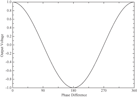
where Km is a constant describing the conversion loss of the mixer. Equation (12.3) is a time-varying cosine waveform at the beat note frequency. When the two frequencies are identical, the output voltage is a function of the phase difference, Δϕ = ϕ1 − ϕ2:
This is maximum when Δϕ = 0 °, a minimum when Δϕ = 180 °, and zero when Δϕ = 90 ° or 270 ° (Fig. 12.3).
FIGURE 12.3 Phase detector voltage output as function of phase difference.
In the frequency domain, the phase detector can be modeled as
(12.5)
![]()
which at low frequencies is simply the slope of the voltage versus phase curve. The units for Kpd is V/rad:
Thus, Kpd = 0 when Δϕ = 0 ° or 180 ° and is at its extreme values at Δϕ = 90 ° or 270 °.
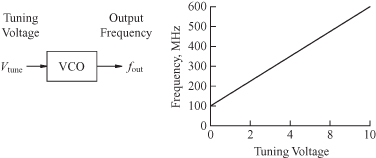
12.5.2 Voltage-Controlled Oscillator
The voltage-controlled oscillator is the PLL control element in which the output frequency changes monotonically with its input tuning voltage. A linear frequency versus tuning voltage is an adequate model for understanding its operation (Fig. 12.4):
FIGURE 12.4 Voltage-controlled oscillator tuning.
In a PLL, the ideal VCO output phase may be expressed as
where ϕ2(t) is the output phase of the VCO, ω0 is the free-running VCO frequency when the tuning voltage is zero, and Kvco is the tuning rate with the dimension of rad/s-V.
The error voltage from the phase detector first steers the frequency of the VCO to exactly match the reference frequency, then holds it there with a constant phase difference. It is modeled as having a low-frequency gain Kvco and one or more poles of the following form:
(12.9)
![]()
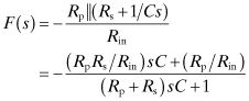
12.5.3 Loop Filters
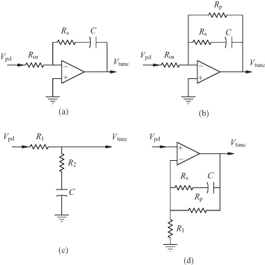
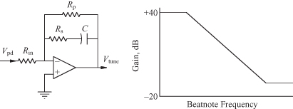
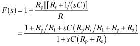
A loop filter is a low-frequency circuit that filters the phase detector error voltage, which in turn controls the VCO frequency. The filter may be either active or passive, but it is usually a simple analog design. In extreme cases it might be an entire microprocessor. This discussion will be limited to analog loop filters such as the representative topologies shown in Fig. 12.5. Figure 12.5a shows an op-amp integrator with nearly infinite dc gain. This is the loop filter often associated with the type 2 PLL. The order and type of a PLL is defined in Section 12.9. Figure 12.5b shows an operational amplifier loop filter with a finite gain and is associated with a type 1 PLL. Figure 12.5c is a passive filter used with a phase detector whose output is current rather than voltage. This type of detector is frequently found in synthesizer ICs and is associated with a type 2 PLL. While the loop filter is a simple circuit, its characteristic is important in determining the final closed-loop operation. The wrong design may make the loop unstable, causing oscillation or have an undesirable response. The loop filters shown in Fig. 12.5 are of the form
(12.10)
![]()
where −a is a zero and −b is a pole.
FIGURE 12.5 Loop filter used in (a) type 2 second-order PLL, (b) type 2 third-order PLL, (c) type 1 second-order PLL, and (d) type 1 second-order inverting PLL.
12.5.4 Frequency Dividers
When the output frequency must be a multiple of the input frequency, frequency dividers may be included in a PLL. Most dividers use a digital circuit, although analog techniques dating from 1939 are available for very high frequency devision. With the availability of complete synthesizers on a single IC, fewer stand-alone divider circuits are on the market. Most dividers have a division ratio equal to a binary number or switchable from a binary to a binary +1 (e.g., divide by 64 or 65). The upper limit on the input frequency is about 3 GHz, although only a few ICs will go that high. Divide by four circuits have been demonstrated with inputs above 14 GHz, but this is a very specialized device not required by most PLLs. For a linear analysis when the loop bandwidth is much less than the reference frequency, dividers are modeled as a gain element with a value = 1/N.
12.6 LINEAR ANALYSIS OF THE PLL [5]*
From the perspective of the time domain, the control voltage for the VCO is
where f(t) is the impulse response of the filter and Ve is the error voltage coming from the phase detector. The Laplace transform of f(t) is
(12.12)
![]()
and the inverse transform can be obtained in principle by the integral:
(12.13)
![]()
Substituting Eq. (12.11) into the derivative of Eq. (12.8) gives the VCO frequency:
(12.14)
![]()
where Δϕ(t) = ϕ1(t) − ϕ2(t). Consequently, a general equation describing the phase error is
(12.15)
![]()
For a given input phase ϕ1, the solution of this equation describes the exact operation of the PLL. However, to avoid carrying along ω0, a new phase variable may be defined:
The equation for the phase error is now given without ω0:
This suggests an alternate representation for the phase-lock loop as shown in Fig. 12.6. In this representation the multiplier is replaced by a subtracter and a cosinusoidal nonlinearity while the VCO is replaced by an integrator.
FIGURE 12.6 Time-domain nonlinear phase-lock loop.
When the phase error Δϕ deviates from 90 ° by a small amount, cos(Δϕ − 90 °) ≈ Δϕ. Then Eq. (12.18) becomes
where
(12.20)
![]()
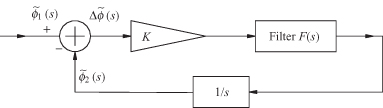
If the Laplace transform of ψ1(t) is represented by ![]() and the Laplace transform of Δϕ(t) is represented by
and the Laplace transform of Δϕ(t) is represented by ![]() , then the Laplace transform of Eq. (12.19) is
, then the Laplace transform of Eq. (12.19) is
(12.21)
![]()
This linear frequency-domain equation for the PLL can be represented as shown in Fig. 12.7. The solution for the phase error gives
FIGURE 12.7 Frequency-domain linear phase-lock loop.
so that the phase shift at the output of the PLL is
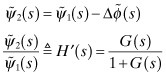
where G(s) = KF(s)/s. The phase error can in turn be written in terms of this phase transfer function:
This is the difference of the two phase terms entering the phase detector. A frequency multiplier circuit will incorporate a frequency divider in the feedback loop, so that K → KN. However, the output will differ from ![]() by the frequency multiplier factor, N, and the transfer function from input to output is
by the frequency multiplier factor, N, and the transfer function from input to output is
For example, let N = 1, the phase of the incoming signal be given by ϕ1(t) = ωt + ϕ0, and the PLL has no filter so that F(s) = 1. Readjusting the phase reference as was done in Eqs. (12.16) and (12.17) gives
(12.26)
![]()
(12.27)
![]()
In the frequency domain this becomes
(12.28)
![]()
The phase error is found from Eq. (12.22):
(12.29)
![]()
The inverse transform in this case is straightforward and gives the phase error in the time domain:
(12.30)
![]()
The steady-state phase error is found by allowing t → ∞:
(12.31)
![]()
Clearly, the phase will change when the incoming frequency changes, so that phase lock is not achieved.
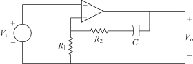
The insertion of a low-pass filter into the PLL will produce lock. An active filter such as that shown in Fig. 12.8 is recognized as basically a noninverting amplifier. The inverting amplifier would have right half-plane poles in the PLL and is therefore unstable unless the VCO or phase detector circuit can accommodate the minus sign. For the noninverting case, the voltage transfer function can be found by writing node equations at the input nodes of the operational amplifier:
(12.32)
![]()
FIGURE 12.8 Possible active low-pass filter for PLL.
The phase transfer factor is found from Eq. (12.23):
(12.33)
![]()
Thus, using Eq. (12.24), the phase error is easily obtained:
(12.34)
![]()
(12.35)
![]()
Rather than find the inverse transform this time, the final value theorem may be used to find the steady-state phase error:
(12.36)
![]()
In this case, the phase error is independent of frequency and in the steady state is zero.
12.7 LOCKING A PHASE-LOCK LOOP
The previous sections examined the individual elements of a PLL. A simple loop with no frequency divider will serve as an example of how these parts work together. Assume that initially the loop is not locked, and the reference frequency is 100 MHz. A tuning voltage of 5 V is required to make the VCO frequency operate at 100 MHz. The phase detector can produce a cosine wave beat note of 1 V peak to peak.
An inverting op-amp type 1 loop filter will be used with a gain of 100 at low frequency and a gain of 0.1 at high frequency (Fig. 12.9). With the loop unlocked, the VCO frequency could be anywhere within its operating limits. Assume that it is operating at 101 MHz, so that there is a 1-MHz beat note at the phase detector output when the reference frequency is first applied. This beat note frequency is high enough to only be amplified with a gain of 0.1 by the loop filter. The VCO tuning voltage will be modulated by the phase detector output of 0.1-V peak to peak, but this voltage will not cause any significant change in the VCO frequency.
FIGURE 12.9 (a) Type 1 loop filter and (b) its frequency response.
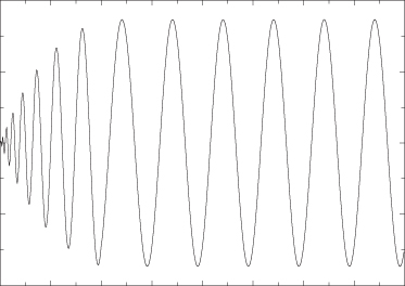
Since the VCO frequency is too far away from the reference frequency, there is not enough gain in the loop to bring the loop into lock. However, if the VCO frequency is 100.1 MHz when the reference frequency is applied, the beat note frequency is 100 kHz. That is well within the high-gain frequency range of the loop filter for this design. The amplified beat note voltage modulates the VCO frequency. As the VCO frequency swings closer to the reference frequency, the beat note frequency gets even lower, and it enters an even higher gain region of the loop filter. This action accelerates the VCO frequency change until it crosses the reference frequency. At this point the beat note frequency is zero. The PLL has been designed as a stable closed-loop system, and the VCO is at the same frequency as the reference. The transient phase detector output voltage and the VCO tuning voltage are shown in Figs. 12.10 and 12.11, respectively. The input voltage to the VCO is 5 V when the PLL is at frequency lock. Since the loop filter has a dc inverting gain of 100, the voltage at the phase detector output is
FIGURE 12.10 Phase detector voltage as PLL pulls into lock.
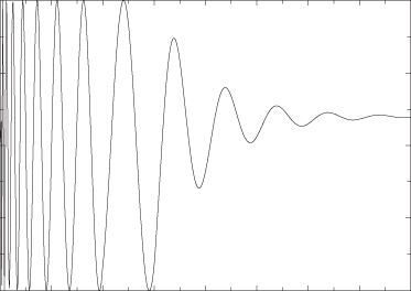
FIGURE 12.11 VCO tuning voltage as PLL pulls into lock.
The maximum voltage from the phase detector was specified to be 1 V peak to peak or Ve = 0.5 V from the zero level to the peak. This would occur when Δϕ = 0 ° as specified by Eq. (12.4). This equation then gives the value for KmVaVb = 1. When Ve = −50 mv as given in Eq. (12.37) the value for the phase difference from Eq. (12.4) is Δϕ = arccos(2Ve/KmVaVb) = arccos(−0.1) = 95.7 °. The loop filter will keep the VCO at 100 MHz and maintain a 95.7 ° phase difference between the two phase detector inputs.
An oscillator accumulates 360 ° of phase rotation in each cycle. If the frequency increases, it will accumulate more phase rotation in a given period of time. If the VCO tries to drift higher in frequency, it will quickly accumulate more phase rotation. The phase detector output voltage will go up, and the loop filter will amplify this change, which will lower the VCO control voltage. The VCO output frequency will drop and return to 100 MHz. The situation is similar for the VCO trying to move lower in frequency. This is the effect of the negative feedback within the loop. The battle for control goes on continuously. Small changes in the VCO due to temperature, noise, or even gravity cause small frequency changes. The PLL will not tolerate errors due to frequency or phase changes. When an error voltage develops at the phase detector output, the loop filter will amplify it and the VCO frequency and phase will return to the correct value. The corrective action of the loop will make whatever adjustments are required to hold the phase and frequency constant.
The initial beat note frequency must be well within the loop filter bandwidth to achieve lock without frequency aiding. In any loop, the first event is to bring the VCO frequency in line with the reference frequency. Once the circuit is in lock, a steady-state phase relationship that satisfies the loop feedback and dc requirements is found that will hold its lock frequency.
12.8 LOOP TYPES
The PLL is a closed-loop system controlled by negative feedback. The closed-loop gain H(s) for the circuit in Fig. 12.7 is described by
where G(s) is called the open loop or forward gain, and G(s)/N is called the loop gain. The forward gain is the product of the phase detector gain, the loop filter gain, and the VCO gain, that is, G(s) = KF(s)/s. The frequency divide ratio is N.
At every point in the loop, the signal has a voltage amplitude and a phase. The function, H′(s), from Eq. (12.23) represents a ratio of two phase terms. The G(s) function can be seen as converting a phase to a voltage in the phase detector and converting voltage to a phase in the VCO. The frequency divider simply multiplies the output of G(s) (a phase or frequency) by 1/N. The functions G(s) and N are both dimensionless quantities.
The number of pure integrators (or number of poles at the frequency origin) in the loop gain G(s)/N determines the type of the system. A VCO is a pure phase integrator that will contribute one pole to the type determination. Therefore, a PLL will be at least type 1. A loop filter with a finite dc gain will not increase the type number. A loop filter with an integrator such as that in Fig. 12.5a, will increase the type to 2.
The order of the PLL is the degree of the denominator polynomial of Eq. (12.38). The loop filter operational amplifier has at least two significant break points: typically one at a frequency between 1 Hz and 100 kHz and a second above 10 MHz. In the example given in Section 12.7 that used a type 1 loop, the only pure integrator is the VCO, so there is only one pole at dc. The loop filter has a dc inverting gain of 100. If the VCO gain is 1 MHz/V and the reference frequency is changed to 103 MHz, the VCO tuning voltage will now be 8 V. This is found from fref = fout = KvcoVtune + f0 where Vtune = 5 gives f0 = 95 MHz. Thus, when fref = 103 MHz, Vtune must be 8 V. With a gain of −100, the phase detector voltage must be Ve = 8/(−100) = −80 mV.
This represents an angular difference of Δϕ = arccos(2Ve/KmVaVb) = 99.2 ° in contrast to 95.7 ° found earlier when the reference frequency was 100 MHz. If the reference frequency continues to change, the VCO frequency will change to match it, which in turn will change the phase detector output voltage. As the reference frequency changes in a type 1 loop, the phase difference changes. This is an important characteristic that is sometimes desirable and other times unacceptable.
If the dc gain of the loop filter is increased to 1000, the phase detector output voltage for a 100-MHz lock is only −5 mV. For phase lock at 103 MHz the phase detector output voltage is −8 mV. These values represent phase differences, Δϕ, of 90.57 ° and 90.92 °, respectively. If the dc gain is further increased, the change of Δϕ with frequency will further decrease. Finally, the dc feedback resistor, Rp, will approach an open circuit and the loop filter dc gain will increase to infinity. The loop filter in Fig. 12.5b is transformed to that shown in Fig. 12.5a.
This loop filter is now a pure integrator, thereby producing a type 2 loop. The total number of integrators for the PLL with this loop filter is two: one for the VCO and one for the loop filter. Among the features of this loop is the constant phase shift between the VCO and reference frequency that is maintained with a change in frequency.
Type 1 and type 2 loops constitute the majority of applications. Type 3 and higher loops are required to solve frequency change problems in unusual situations. For example, a ground-launched missile must track an orbiting satellite during its own launch and orbital insertion. During the launch phase, the rocket is consuming fuel and thus reducing its mass. With a constant force, its acceleration will increase at an increasing rate. As the satellite comes overhead, its transmit frequency is shifted due to the relative motion with the rocket. This shift is changing at an increasing rate. Then the booster separates from the rocket and the force goes to zero during coast. To track the satellite frequency with no phase error requires a PLL type of at least 4. Most high-type loops are used to solve complicated motional problems.
12.9 NEGATIVE FEEDBACK IN A PLL
A frequency change that generates a change in the phase of a stable negative feedback loop generates a correction for the phase error. In the previous example, the type 1 loop filter was described as having a dc inverting gain of 100. The VCO requires 5 V to produce a 100-MHz output. An open-loop connection of the PLL components will demonstrate what is called the “sense” of the loop. For open-loop testing, the VCO is connected to a manually adjustable power supply. With the power supply set at 5 V, there will be a low-frequency beat note observed at the phase detector output. If the voltage is changed to either 4 or 6 V, the beat note will be 1 MHz. The frequency of the VCO cannot be determined from the beat note, since the beat note shows only the frequency difference between the two signals and not which signal is the higher or lower frequency. A complete description of the difference frequency between the VCO and reference requires both a direction and a magnitude. With the loop out of lock, this type of phase detector can only determine the magnitude, |Δϕ|. The VCO frequency must be forced close enough to the reference frequency for the beat note to be inside the loop bandwidth for a PLL with this type of phase detector to pull into phase lock.
In the previous example with the inverting filter, the VCO frequency increased as the tuning voltage decreased as seen from Eq. (12.7) where Kvco < 0. Many VCOs have the opposite characteristic; that is, the frequency increases with increasing tuning voltage. Stability is assured by the appropriate choice of an inverting or noninverting filter. If the loop locked up at 90 ° difference between the two inputs with the positive slope VCO, it will lock up at 270 ° with the negative slope VCO. The phase detector output in either case will be correct to adjust the VCO to match the reference input frequency and phase.
Most synthesizer ICs and PLLs using frequency dividers or logic ICs have a different type of phase detector. Using flip-flops to count the input edges, these phase detectors produce an error voltage that has not only a magnitude but also a sense of the direction between the two inputs. The output is a series of voltage or current pulses. The loop filter averages these pulses to form the control voltage for the VCO. A pulse duty cycle above 50% indicates that the VCO frequency is higher than the reference frequency, and a duty cycle of less than 50% indicates that the VCO frequency is lower. If the VCO is running higher than the reference frequency, the control voltage will force it toward the correct value. If the VCO is running too low, the error voltage will drive the frequency higher. This type of phase detector can drive a PLL into lock even when the VCO and reference frequencies are a great distance apart, far outside the loop bandwidth. The typical IC synthesizer will have a pin available to reverse the sense of the error voltage to accommodate VCOs of either positive or negative tuning slope.
12.10 PLL DESIGN EQUATIONS
Each block of the normal phase-lock loop model (Fig. 12.12) is described by a gain value that may be a constant or a function of frequency. The components are carefully selected to ensure a locking mechanism and stable loop operation. The frequency response of the closed loop is typically displayed as a Bode plot with a minimum frequency of 1 Hz and a maximum frequency between 10 kHz and 10 MHz. The Bode plot describes the filtering bandwidth and in turn the transient response of the PLL to the input voltage.
FIGURE 12.12 Frequency-domain closed-loop model for PLL.
12.10.1 Inverting Loop Filter
An inverting filter, such as that shown in Fig. 12.5b, produces a 180 ° phase shift between its input and output. The VCO would have to match the filter so as to produce an increase in frequency with a decrease in voltage. Thus, with either an inverting filter or a noninverting filter, the phase transfer function given by Eq. (12.25) remains:
The example that follows makes use of a second-order type 1 PLL. The transfer function for the filter in Fig. 12.5b is
The open-loop gain is
When Eqs. (12.40) and (12.41) are substituted into the expression for the the closed-loop PLL [Eq. (12.39)], the result is clearly of second order in the denominator. This can be written in terms of notation commonly used in control theory:
(12.42)
![]()
The variable, ζ, is the damping ratio and ωn is called the natural frequency. The roots of the denominator are
(12.43)
![]()
For the second-order type 1 loop under consideration,
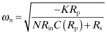
so that
The design specification for a PLL is typically given in terms of a damping ratio and a natural frequency. The design task is to determine circuit values that will meet the specification. The filter response at dc is
(12.47)
![]()
where the minus sign is to be absorbed by K. Thus, Eq. (12.45) can be rearranged to give
and this substituted into Eq. (12.46) to give
(12.49)
![]()
Using Eq. (12.48) to replace Rs above gives,
If, in addition to the damping ratio and the natural frequency, values for C and the dc gain are chosen, then the required resistance values can be found as summarized below. Solution of Eq. (12.50) gives the value for Rp, then Rs, and finally Rin:
(12.52)
![]()
(12.54)
![]()
To guarantee Rp > 0, the first two terms in the brackets of Eq. (12.51) must be more negative than the third term. Since K < 0 for a PLL with an inverting filter, Rp would be positive. Thus
To guarantee Rs > 0, the first term in Eq. (12.53) must be more negative than the second terms:
These two inequalities lead to the following conclusion:
Comparing the first and last inequalities of Eq. (12.57) gives Fdc < 0, which was assumed at the outset. However, Eqs. (12.55) and (12.56) give the explicit requirements for Rp and Rs.
Figure 12.13 illustrates the expected PLL bandwidth versus frequency for several values of damping ratio in a typical second-order circuit. These results are calculated for a natural frequency of 1 Hz. The results can be easily scaled for loops requiring higher natural frequencies. When ζ < 1, the PLL is underdamped and peaking occurs. The response of such a loop to a disturbance will be a damped oscillation that finally converges to the final answer. When ζ > 1, the system is overdamped. The −3-dB frequency is found by setting the transfer function to ![]() and solving for ω3/ωn. It is assumed in doing this that only the denominator terms are frequency dependent. Thus,
and solving for ω3/ωn. It is assumed in doing this that only the denominator terms are frequency dependent. Thus,
(12.58)
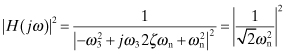
FIGURE 12.13 PLL response with natural frequency of 1 Hz and various damping ratios.
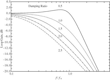
Therefore,
The −3-dB gain frequency, f3, for a damping ratio of 1.0 is 0.6436 times the natural frequency. If a −3-dB frequency of 50 kHz were required with a damping ratio of 1.0, then a natural frequency of 77.889 kHz would be chosen.
A type 2 PLL can be formed by allowing Rp → ∞ to give the filter shown in Fig. 12.5a. Equation (12.44) becomes
(12.60)
![]()
and from Eq. (12.45)
(12.61)
![]()
which gives
Consequently,
12.10.2 Noninverting Loop Filter
Design equations can be developed for a noninverting loop filter like that shown in Fig. 12.5d. The filter transfer function is
The closed-loop gain is found by substituting Eq. (12.64) into Eq. (12.38):
(12.65)
![]()
From this the loop natural frequency and damping ratio can be identified:
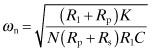
The typical synthesis procedure is to design a PLL for a given natural frequency and damping ratio using a specified capacitance, C. Solving Eq. (12.66) for Rp + Rs and substituting this into Eq. (12.67) gives an equation in terms of one unknown, Rp. First, from Eq. (12.66),
then substitution gives
(12.69)
![]()
This has one unknown, Rp, which can be solved by the quadratic formula as follows:
(12.70)
![]()
where
(12.71)
![]()
(12.72)
![]()
(12.73)
![]()
so that
The value of R1 is associated with the dc voltage gain of the noninverting loop filter:
(12.75)
![]()
The value for Rs is obtained from Eq. (12.68). Physically realizable solutions would require the discriminant of Eq. (12.74) to be positive. This can be found in terms of the PLL parameters:
(12.76)
![]()
The type 2 PLL parameters with the noninverting loop filter can be found by letting Rp → ∞. Thus, the design equations for a given natural frequency, damping ratio, and capacitance for a type 2 PLL are
(12.77)
![]()
or
(12.78)
![]()
and the damping ratio is
(12.79)
![]()
or
(12.80)
![]()
The value for K is given by Eq. (12.41). A second-order loop can be built either as a type 1 or a type 2 with either an inverting or noninverting loop filter. The actual loop order may be several orders higher than 2 when all the extraneous poles are considered. A good design procedure initially ignores these poles and assumes ideal VCOs, phase detectors, operational amplifiers, and the like and determines a set of loop filter values based on the second-order model. Subsequently, nonideal parts can then be added and computer simulation used to refine the analysis.
12.11 PHASE DETECTOR TYPES
Previous sections have introduced both the mixer and flip-flop-based phase detectors. These two widely used configurations have many specialized variations. A sampling phase detector is a third type that is frequently used in RF and microwave applications. The design requirements for a specific application will usually point to the correct choice.
12.11.1 Mixer Phase Detectors
Mixers with a dc-coupled output make an excellent phase detector. At high frequencies, a mixer may be either active (with transistors) or passive (with diodes). The diode versions usually provide the best dc stability. It is the best choice for low-noise designs where the PLL reference input is a low-level signal. The beat note output is typically 100 mV to 1 V peak to peak, depending on the mixer type and application. The mixer type phase detector is the best choice when the input signal is pulsed or noncontinuous. The ability of this type of detector to resolve an angular difference is limited to ±90 °. It has no ability to determine which input is the higher frequency, so it is not capable of frequency discrimination.
12.11.2 Sampling Phase Detectors
Sampling phase detectors (SPD) can be used in a phase-lock loop to produce an output frequency that is an integer multiple of the reference frequency. This mixer relies on a device to generate a comb of frequencies at multiples of the reference. The VCO then uses the correct spectral line to produce an error signal. An SPD is used in a phase-lock loop where the output frequency is an integer multiple of the input frequency. If fout = Nfin + Δf, the SPD output is a cosine wave of frequency Δf. If fout is exactly N times fin, the SPD output is a dc level proportional to the phase difference between its two inputs. The input frequency, fin is typically between 50 and 200 MHz at a power level of +20 dBm or higher, and fout can be at any harmonic of fin up to about 18 GHz or up to about the 150th harmonic of fin.
A sampling phase detector is one of the best choices for a very high frequency PLL where excellent phase noise is a requirement. However, an external circuit is usually required to bring the VCO into lock range. Additionally, provisions must be made to ensure that the VCO will be locked to the correct multiple of fin.
12.11.3 Flip-Flop Phase Detector with Frequency Acquisition Aiding
All of the phase detectors previously discussed have a major drawback. They produce an output equal to the difference between the two input frequencies, either a cosine wave or a triangle wave. However, this output does not have information about whether the VCO is too high in frequency or too low. A PLL using these phase detectors must also include a sweep or search circuit to initially bring the VCO frequency close enough to lock. This can involve a substantial amount of circuitry. The phase detector circuit shown in Fig. 12.14a uses positive edge triggered D-type flip-flops to overcome this problem. The D inputs are connected to a logic 1. Figure 12.14b illustrates the timing sequence. The signal, f1, positive edge arrives first, causing Q1 to clock high. Later the positive edge of f2 causes Q2 to clock high. Two 1’s at the NAND gate’s input cause its output to go low and clear both Q1 and Q2. The output at Q2 is a pulse whose duty cycle represents the time delay between f1 and f2. The pulse at Q2 is very short since it is the sum of the propagation times through the flip-flops and gates. Of course, if f2 arrives before f1, then the output pictures are reversed.
FIGURE 12.14 (a) Phase detector using a D flip-flop and (b) the timing chart.
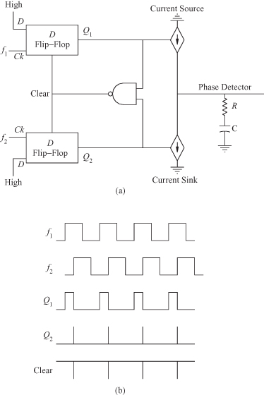
The outputs, Q1 and Q2, turn on the current sources. These current sources either source or sink current to the capacitor, which ramps up or down the phase detector output voltage. The action of this circuit is identical to the op-amp integrator. So the phase detector has added another integrator to the PLL. A PLL using this circuit will be at least a type 2 loop.
The advantage of this circuit is the self-searching capability. If f1 is higher than f2, the output voltage will go to the positive voltage limit. If f1 is lower than f2, the output voltage will go to the negative voltage limit. If f1 equals f2, the output voltage will be proportional to the phase difference. Thus, this circuit can sense which input frequency is higher. The output voltage can then be used to drive the VCO in the correct direction to bring the loop into lock. Once the two frequencies are the same, this circuit becomes a phase detector and drives the VCO for no phase error.
This phase detector circuit is used in many present-day frequency synthesizer ICs, where its built-in search capability makes it ideal for a variety of applications. However, there are at least two drawbacks to this circuit that limits its usage. The largest problem is the short pulse on one of the flip-flop outputs. With high-speed logic, this pulse is only a few nanoseconds long. If f1 and f2 are high in frequency, this pulse width may be a significant part of their period. The pulse dead time due to propagation delays results in a nonlinear phase detector transfer curve. In older versions, there were flat spots with zero gain and regions where the gain reversed its slope. The pulse also contributes heavily to the output noise, easily adding 20 dB of noise to the PLL output even in the most modern devices. The second problem is that the searching capability can become confused if there is any interruption in either f1 or f2. Therefore, this circuit should be used in applications where very low phase noise is not required and the inputs are continuous. For this phase detector the gain is Kpd volts/rad.
12.11.4 Exclusive OR Phase Detector
An exclusive OR gate works as a frequency doubler and phase detector. Figure 12.15 illustrates a typical example for the phase detector. For correct operation, both inputs, f1 and f2, must be at the same frequency and both must have 50% duty cycles. The XOR output will be a logic level waveform at twice the input frequency. The duty cycle of the output depends on the phase difference between the two inputs. Phase shifts of 90 ° or 270 ° produce a 50% duty cycle output. The RC low-pass filter produces a dc value proportional to the duty cycle. For a 90 ° or a 270 ° phase difference, the filter output is one half the difference between the logic high- and logic low-output voltages.
FIGURE 12.15 Exclusive OR phase detector.
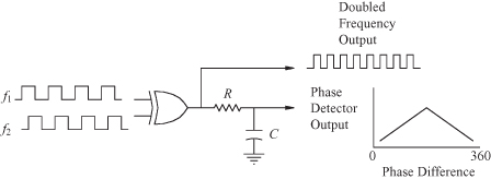
The XOR gate is the functional equivalent of the balanced mixer. This circuit is useful for PLL applications requiring a high-frequency VCO to be divided down and locked to a low-frequency logic-level frequency reference. This phase detector is suitable for low phase noise applications, but it frequently requires an external search circuit to initially achieve lock.
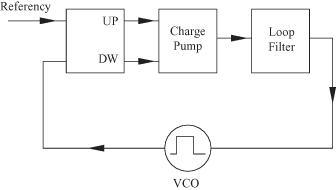
12.11.5 Charge Pump PLL
The charge pump phase-lock loop described by Gardner [6] incorporates a digital phase/frequency detector (PFD) plus a charge pump that basically converts the digital output voltage to an analog current. This in turn is fed to the loop filter. The block diagram is shown in Fig. 12.16 where the PFD has a three-state digital logic output of up, down, and neutral (UP, DW, and N).† This is fed into a charge pump that charges or discharges the loop filter capacitance depending on whether the output logic is UP or DW. If the phase detector is N, the loop is locked and no current flows. The loop filter can be as simple as a shunt capacitance to ground or something like that shown in Fig. 12.5c.
FIGURE 12.16 Charge pump phase-lock loop.
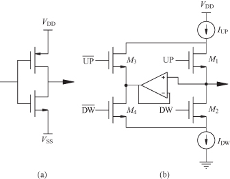
There are a wide variety of charge pump circuits, two of which are shown in Fig. 12.17. The first of these uses positive and negative voltage logic states that charges or discharges the loop filter, depending on the state of the PFD. It is possible for both transistors to be off so that the voltage on the loop filter is floating. The operational amplifier in Fig. 12.17b helps to control this voltage. This circuit, as drawn, uses positive and 0 voltage logic states. When UP is high and DW is 0, transistors M1 and M4 are on and M2 and M3 are off. Current IUP charges the loop filter and IDW draws current through M4 and the low-impedance output of the operational amplifier. The opposite transistors turn on when DW is high and UP is 0, and the loop filter is discharged. The operational amplifier must be capable of handling the current levels of the current sources. Several advanced designs have been proposed that address the floating voltage, the additional complexity of the operational amplifier, and nonideal components [7–9].
FIGURE 12.17 Example charge pump circuits.
12.12 DESIGN EXAMPLES
Example 1
A phase-lock loop design shown in Fig. 12.18 requires an output frequency of 1600 MHz where the reference oscillator is 100 MHz. The design approach chosen is to use an inverting type 2 loop filter with a frequency divider and a mixer phase detector. The VCO chosen shows a typical tuning slope of 1 MHz/V. Measurement of the phase detector output shows a 100-mV peak to peak cosine wave. The filter is to have a 3-dB bandwidth of 100 kHz with a damping ratio of 1.
a. Using a 100-pF capacitor, find the remaining loop filter values.
b. Using a 10-kΩ Rin, find the remaining loop filter values.
FIGURE 12.18 PLL for Example 1.
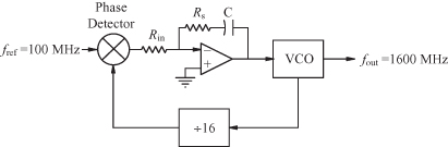
Solution 1
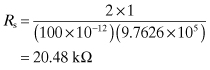
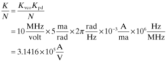
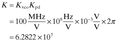
From the graph in Fig. 12.13 the 3 dB frequency for a damping ratio ζ = 1 is f/fn = 0.6435 so that fn = 100 kHz/0.6436 = 155.38 kHz and ωn = 976.26 · 103 rad/s. The type 2 circuit for this example is shown in Fig. 12.16. The output frequency is 16 times the input frequency so N = 16. The value for Kvco is specified to be at 1 MHz/V. The phase detector output is a cosine wave. If the loop locks at 90 ° or 270 °, the phase detector output voltage is zero. For a positive Rin, the slope is the first derivative evaluated at 270 °, so that from Eq. (12.6)
![]()
The 50 mV/rad comes from the 100-mV peak to peak specification. The value for K/N is
(12.81)
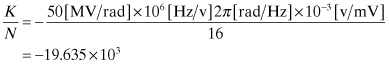
For part (a). where C is set at 100 pF, Eqs. (12.62) and (12.63) are to be used:
(12.82)
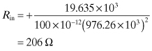
and
(12.83)
Example 2
A synthesizer design shown in Fig. 12.19 requires an output frequency from 900 to 920 MHz. The output frequency can be changed in 1 kHz steps by changing the divide ratio. Design a PLL using a synthesizer IC and an external VCO. The synthesizer IC data sheet lists the current mode phase detector output as 5 mA/rad. The VCO data sheet lists the tuning rate at 10 MHz/V.
FIGURE 12.19 Synthesizer design for Example 2.
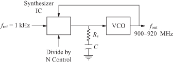
Solution 2
The output frequency must be an integer multiple of the reference frequency so the reference frequency is 1 kHz. The circuit diagram is shown in Fig. 12.19. The divide ratio must change from 900 MHz/1 kHz or 9 × 10⁵ to 920 MHz/1 kHz or 9.2 × 10⁵. The midpoint value, 9.1 × 10⁵ can be used for the design. A damping ratio of 1 is chosen for a rapid settling time when the divide ratio changes. The loop filter must attenuate the pulses from the phase detector output running at 1 kHz. Figure 12.13 shows that 14 dB of attenuation can be expected at 10 times the natural frequency. With a slope of −20 dB/decade, 34 dB attenuation can be expected at 100 times the natural frequency. Choosing fn = 10 Hz or ωn = 62.83 rad/s will work with a 1-kHz reference frequency. Here the value of K is in dimensions of ampere/volt:
The VCO is assumed to have a high input impedance so that the ratio of the voltage, Ve, seen at the input of the VCO to the input current i is
![]()
The phase transfer function is found from G(s):
![]()
where
![]()
Thus,
From Eq. (12.84) K = ω2 and 2ζωn = KCR2 so that
![]()
which gives for C = 100 μF and ζ = 1, R2 = 318 ![]() .
.
Example 3
A frequency synthesizer contains a phase-lock loop circuit that uses a type 1 noninverting filter. The data sheets for the phase detector show that the output waveform has a slope of 100 mV/rad. The VCO nominal output frequency is 3 GHz with a tuning rate of 100 MHz/V. The reference is a 100-MHz crystal oscillator. If Rin = 620 ![]() , Rs = 150
, Rs = 150 ![]() , Rp = 56 kΩ, and C = 1 nF, what is the expected 3-dB bandwidth and damping ratio for this PLL?
, Rp = 56 kΩ, and C = 1 nF, what is the expected 3-dB bandwidth and damping ratio for this PLL?
Solution 3
With a 3-GHz output and a 100-MHz reference, the frequency divide ratio N must be 30:
and
![]()
For the noninverting loop, Eq. (12.66) gives the natural frequency:
![]()
and from Eq. (12.67):
![]()
Finally, the 3-dB frequency for the loop is found from Eq. (12.59):
![]()
Thus, the 3-dB frequency is f3 = 292.9 kHz. This can be confirmed from the curve in Fig. 12.13. A linear interpolation for the 3-dB normalized frequency when ζ = 0.709 is found from Fig. 12.13 to be approximately 1. The natural frequency for this PLL is approximately ωn/2π = 293.7 kHz.
12.13 CONCLUSIONS
Chapter 1 began with a description of a generic superheterodyne transmitter–receiver pair. Each of the components in that block diagram were analyzed using a variety of circuits often requiring special RF design techniques. Passive circuit elements had to be chosen with care because of their stray inductance, parasitic capacitance, skin effect losses, and the like. A large amount of attention was given to filters and impedance transformers. Filters control the bandwidth and are necessary to avoid transmitting unwanted signals and receiving extraneous interference or noise. Impedance matching played a crucial role in determining the gain, stability, and noise figure of amplifiers as well as design of oscillators. The discussion of transmitter power amplifiers described the pros and cons of different types of amplifiers and provided analytical guidelines for their design. Low-phase noise oscillators supply the transmitter carrier frequency by exciting the LO port of a mixer. The modulator and demodulator scheme takes on a wide variety of forms in communication circuits, both analog and digital. The basic forms given in Chapter 11 provide the basic theory for mixers. Not found explicitly on the transceiver block diagram is the phase-lock loop described in this final chapter. Nevertheless, they are pervasive in RF designs and, for example, often are used to lock the frequency of the transmitter and receiver together. The journey does not conclude here, for there are a multitude of applications and designs that were left out, and others yet to be discovered. What was provided in this book is the background for further study and invention.
PROBLEMS
12.1. A phase-lock loop can be described in the frequency domain in terms of the input and output phase angles shown in Fig. 12.7. The input phase is ![]() . The filter transfer function is
. The filter transfer function is
![]()
a. What is the steady-state phase error?
b. What is the steady-state phase error if the capacitance C = ∞?
12.2. The circuit in Fig. 12.7 has an input signal with a phase that varies as ![]() , where ω0 and ϕ0 are offset constant values. The filter has a transfer function given by F(s) = 2 + 10/s2. Determine if this loop provides phase lock. If not, determine if it provides frequency lock.
, where ω0 and ϕ0 are offset constant values. The filter has a transfer function given by F(s) = 2 + 10/s2. Determine if this loop provides phase lock. If not, determine if it provides frequency lock.
Notes
* This material is based on A. J. Viterbi, Principles of Coherent Communication, 1966, by permission of The McGraw-Hill Companies.
† See, for example, the Max9382 PFD from Maxim.
REFERENCES
1. U. L. Rhode, Microwave and Wireless Synthesizers, Theory and Design, New York: Wiley, 1997.
2. J. A. Crawford, Frequency Synthesizer Design Handbook, Norwood, MA: Artech House, 1994.
3. U. L. Rhode and J. C. Whitaker, Communications Receivers, 3rd ed., New York: McGraw-Hill, 1996.
4. B. Razavi, Monolithic Phase-Locked Loops and Clock Recovery Circuits, New York: IEEE Press, 2001.
5. A. J. Viterbi, Principles of Coherent Communication, New York: McGraw-Hill, 1966.
6. F. M. Gardner, “Charge-Pump Phase-Lock Loops,” IEEE Trans. Commun., 28, pp. 1849–1858, Nov. 1980.
7. W. Rhee, “Design of High-Performance CMOS Charge Pumps in Phase-Locked Loops,” Proc. of the 1999 IEEE International Symposium on Circuits and Systems, Orlando, Florida, pp. 545–548, May 1999.
8. R. C. Chang and L-C. Kuo, “A New Low-Voltage Charge Pump Circuit for PLL,” Proc. Of the 2000 IEEE International Symposium on Circuits and Systems, Geneva, Switzerland, pp. V-701–V-704, May 2000.
9. H. Yu, Y. Inoue, and Y. Han, “A New High-Speed Low-Voltage Charge Pump for PLL Applications,” 2005 6th International Conference on ASIC, Shanghai, China, pp. 387–390, Oct. 2005.