
CHAPTER THREE
Impedance Matching
3.1 INTRODUCTION
A major part of RF design is matching one part of a circuit to another to provide maximum power transfer between the two parts. Even antenna design can be thought of as matching impedance of free space to a transmitter or receiver. This chapter describes a few techniques that can be used to match between two real impedance levels. While some comments will be made relative to matching to a complex load, the emphasis will be on real impedance matching. The first part of this chapter will discuss the circuit quality factor, Q. The Q factor is useful in certain matching circuit designs.
3.2 THE Q FACTOR
The circuit Q factor is defined as the ratio of stored to dissipated power in the following form:
(3.1)
![]()
For a typical parallel RLC circuit, the Q becomes
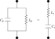
where G is 1/R. For a series RLC circuit,
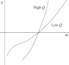
It should be emphasized that Q is defined at circuit resonance. If the circuit reactance is plotted as a function of frequency, the slope of the reactance at resonance is a measure of Q (Fig. 3.1). This is explicitly given as
where B is the susceptance and G the conductance. Alternately,
(3.5)
![]()
where R and X are the resistance and reactance of the circuit. For a series RLC circuit this latter formula will result in the solution given by Eq. (3.3). On the other hand, the Q of a complicated circuit can be readily obtained from Eq. (3.4) or (3.5), numerically if necessary.
FIGURE 3.1 Reactance slope related to Q.
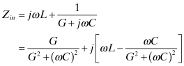
3.3 RESONANCE AND BANDWIDTH
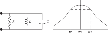
The minimum insertion loss or maximum transmission of a parallel RLC circuit occurs at the resonant frequency of the circuit. When this circuit is excited by a current source, and the output is terminated with an open circuit, the transfer function is
(3.6)
![]()
This is shown in Fig. 3.2. The bandwidth is often defined when the output voltage, Vout, drops from the resonant value by ![]() (or −3 dB). This occurs when the denominator of the transfer function increases from 1/R at resonance to
(or −3 dB). This occurs when the denominator of the transfer function increases from 1/R at resonance to
FIGURE 3.2 Simple parallel resonant circuit.
Equation (3.7) is a quadratic equation in ω2:
Since the resonant frequency is ![]() , and the parallel Q from Eq. (3.2) is ω0C/G = R/ω0L, then Eq. (3.8) can be written in terms of Q and ω0:
, and the parallel Q from Eq. (3.2) is ω0C/G = R/ω0L, then Eq. (3.8) can be written in terms of Q and ω0:
(3.9)
![]()
(3.10)
![]()
The two solutions for ω2 are
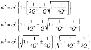
This has been written as a product of two equal terms, so that the original quartic equation has two pairs of equal roots. Taking the square root of Eq. (3.11) provides the two 3-dB frequencies of the resonant circuit:
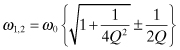
The 3-dB bandwidth of the resonant circuit is the difference between the two 3-dB frequencies:
(3.13)
![]()
The response is clearly not symmetrical about the resonant frequency ω0. The resonant frequency can be found by taking the geometric mean of the two solutions of Eq. (3.12).
(3.14)
However, for narrow bandwidths, the arithmetic mean of the two 3-dB frequencies can be used with small error.
3.4 UNLOADED Q
In real physical reactive elements there are always some resistive losses. The loss in a capacitor or an inductor can be described in terms of its Q. For example, if a lossy inductor is placed in parallel with a lossless capacitor, the Q of the resulting parallel circuit is said to be the circuit Q of the inductor. The inductor Qind then is
(3.15)
![]()
or
(3.16)
![]()
Similarly, for a lossy capacitor, its resistive component could be expressed in terms of the capacitor Qcap. If the inductor, capacitor, and a load resistance RL are placed in parallel, then the total resistance is RT:
(3.17)
![]()
At resonance, XL = XC, so
(3.18)
![]()
The unloaded Q, Qu, is the Q associated with the reactive elements only (i.e., without the load). The bracketed term is the unloaded Q:
(3.19)
![]()
3.5 L CIRCUIT IMPEDANCE MATCHING
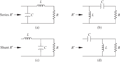
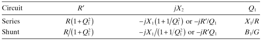
There are four possible configurations that will provide impedance matching with only two reactive elements. In each case, the design of the matching circuits is based on the Q factor, a concept that will become even more important in designing broadband matching circuits [1]. Two of the circuits will be described as the series connection since the reactive element closest to the load resistance is a series reactance (Figs. 3.3a and 3.3b). The circuits with a shunt reactance closest to the load resistance are called the shunt connection (Figs. 3.3c and 3.3d). For the series connection in which the series reactance is an inductance, the total input admittance is given as follows:
(3.20)
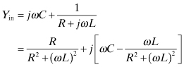
FIGURE 3.3 Four possible L matching circuits.
Resonance occurs when the total shunt susceptance jB = 0. Thus,
(3.21)
![]()
Solution of this for the resonant frequency gives the following expression for the resonant frequency:
(3.22)
![]()
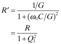
The effect of the load resistor is to modify the resonant frequency somewhat. The conductive part of Yin at this frequency (where B = 0) can be found. Its reciprocal is the input resistance, R′, of the circuit:
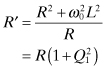
The subscript 1 for Q is present to emphasize this is the first resonator closest to the load. More complicated circuits might have several pertinent Q factors to consider.
At center frequency, the reactance of the series part (i.e., not the capacitance part) will change with changing frequency. Its value can be found from the input admittance expression and is the amount the reactance changes because of the series inductance. This reactance change is
(3.24)
![]()
If X1 represents the series reactance, which in this case is ω0L, then the reactance change of the series element can be found also in terms of Q:
(3.25)
![]()
The second element in the LC section is chosen to resonate out this ![]() :
:
or with Eq. (3.23)
(3.27)
![]()
In the typical synthesis problem, R′ and R are known. Equation (3.23) gives the necessary value of Q1, Eq. (3.3) gives the required L, and Eq. (3.26) or (3.27) gives the required C from X2. This procedure is summarized in Table 3.1.
TABLE 3.1 L Matching Circuit Design Where X1, B1 are Reactance or Susceptance Closest to the Load R
A similar procedure can be applied for the shunt connection in which the shunt capacitance is closest to the load resistance. The input impedance is expressed as follows:
(3.28)
For resonance, the series reactance X = 0. Solution for the resonant frequency for the shunt connection is
(3.29)
![]()
Substituting this back into the input impedance expression gives the input resistance:
(3.30)
The reactance associated with the capacitance is
![]()
Since jX1 = 1/jωC,
(3.31)
![]()
(3.32)
![]()
Since ![]() , the values in Table 3.1 are obtained. The sign of jX2 must always be the opposite of jX1.
, the values in Table 3.1 are obtained. The sign of jX2 must always be the opposite of jX1.
The major feature that should be recognized, whether dealing with elaborate lumped circuits or microwave circuits, if the impedance level needs to be raised, a series connection is needed. If the impedance needs to be lowered, a shunt connection is needed. Furthermore, since the design is based on a resonance condition, the two reactances in the circuit must be of the opposite type. This means two inductors or two capacitors will not work.
3.6 π TRANSFORMATION CIRCUIT
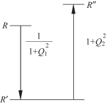
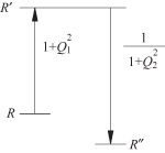
In the previous L matching circuit, the value for Q is completely determined by the transformation ratio. Consequently, there is no independent control over the value of Q that is related to the circuit bandwidth. Addition of a third circuit element gives flexibility to design for bandwidth. If a design begins with a shunt L matching circuit, then addition of another shunt susceptance on the other side of the series element provides the necessary circuit flexibility to be able to choose the circuit Q as a design parameter. The resulting π matching circuit is shown in Fig. 3.4. In this circuit B1 and X2 both act as the impedance transforming elements while the third, B3, is the compensation element that tunes out the excess reactance from the first two elements. As in the L matching circuit, the first shunt element, B1, reduces the resistance level by a factor of ![]() and X2 increases the resistance level by
and X2 increases the resistance level by ![]() where Q2 is a Q factor related to the second element. The final transformation ratio can be R″ < R or R″ > R, depending on which Q is larger as shown in the diagram of Fig. 3.5. To make R″ < R, make Q1 > Q2. The maximum Q, Qmax = Q1, will be the major factor that determines the bandwidth.
where Q2 is a Q factor related to the second element. The final transformation ratio can be R″ < R or R″ > R, depending on which Q is larger as shown in the diagram of Fig. 3.5. To make R″ < R, make Q1 > Q2. The maximum Q, Qmax = Q1, will be the major factor that determines the bandwidth.
FIGURE 3.4 π Impedance transformation circuit.
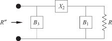
FIGURE 3.5 Diagram showing two-step transformation.
Now consider design of a circuit where R″ < R. Then the first shunt transformation gives
(3.33)
![]()
(3.34)
![]()
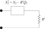
The incremental reactance, X′, is to be added to the series arm. This results in the circuit in Fig. 3.6, which shows that R has been transformed to R′ with a modified series reactance. This series reactance will act to increase the resistance level from R′ to R″. The second transformation Q is
![]()
FIGURE 3.6 Equivalent series reactance after first transformation.
or
(3.35)
![]()
The X2, B3 combination is a series L section with “load” of R′. Consequently,
(3.36)
![]()
(3.37)
![]()
A summary for the design process is shown in Table 3.2. To make R″ < R, make Q1 > Q2 where Q1 = Qmax and follow the design steps in the first column of Table 3.2. For R″ > R, use the second column.
TABLE 3.2 π Matching Circuit Design Formulas
| Step Number | R″ < R | R″ > R |
| 1 | Q1 = Qmax | Q2 = Qmax |
| 2 | ||
| 3 | ||
| 4 | X2 = R′(Q1 + Q2) | X2 = R′(Q1 + Q2) |
| 5 | B1 = Q1/R | B1 = Q1/R |
| 6 | B3 = Q2/R″ | B3 = Q2/R″ |
3.7 T TRANSFORMATION CIRCUIT
The T transformation circuit is the dual to the π transformation circuit and is shown in Fig 3.7. In this circuit, however, the series reactance X1 first raises the resistance level to R′, and the remaining shunt susceptance lowers the resistance level as indicated in Fig. 3.8. The design formulas are derived in the same way as the π circuit formulas and are summarized in Table 3.3.
TABLE 3.3 T Matching Circuit Design Formulas
| Step Number | R″ > R | R″ < R |
| 1 | Q1 = Qmax | Q2 = Qmax |
| 2 | ||
| 3 | ||
| 4 | X1 = Q1R | X1 = Q1R |
| 5 | B2 = (Q1 + Q2)/R′ | B2 = (Q1 + Q2)/R′ |
| 6 | X3 = Q2R″ | X3 = Q2R″ |
FIGURE 3.7 T transformation circuit.
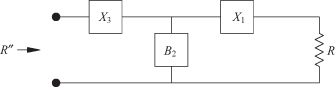
FIGURE 3.8 Diagram showing impedance transformation for T circuit.
3.8 TAPPED CAPACITOR TRANSFORMER
The tapped capacitor circuit is another approximate method for obtaining impedance-level transformation. The description of this design process will begin with a parallel RC to series RC conversion. Then the tapped C circuit will be converted to an L-shaped matching circuit. The Q1 for an equivalent load resistance, Reqv, will be found. Finally, a summary of the circuit synthesis procedure will be given.
3.8.1 Parallel-to-Series Conversion
Shown in Fig. 3.9 is a parallel RC circuit that will be forced to have the same impedance as the series RC circuit, at least at one frequency. The conversion is, of course, valid for only a narrow frequency range, so that this method is fundamentally limited by this approximation.
FIGURE 3.9 Parallel RC to series RC conversion.
The impedance of the parallel circuit is
(3.38)
![]()
The Q for a parallel circuit is Qp = ωCpRp. The equivalent series resistance and reactance in terms of Qp are
3.8.2 Conversion of Tapped C Circuit to an L-Shaped Circuit
The schematic of the tapped C circuit is shown in Fig. 3.10 where R′ is to be matched to R2. The parallel R2C2 section is converted to a series ReqvCeqv, as indicated in Fig. 3.11. Making use of Eqs. (3.39) and (3.40),
(3.41)
![]()
(3.42)
![]()
where Qp = ω0C2R2. Considering R′ as the load, and using the L circuit transformation for a shunt circuit in Table 3.1,
(3.43)
![]()
FIGURE 3.10 Tapped C transformation circuit.
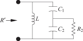
FIGURE 3.11 Intermediate equivalent transformation circuit.
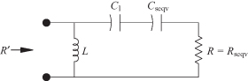
This is the transformed resistance looking through C1 toward the left. Looking toward the right through Cseqv and again using the parallel-to-series conversion Eq. (3.39),
(3.44)
![]()
These two expressions for Rseqv can be equated and solved for Qp:
(3.45)
![]()
3.8.3 Calculation of Circuit Q
An approximate value for Q can be found by equating the impedances of the two circuits in Fig. 3.12:
(3.46)
![]()
FIGURE 3.12 Equate the left- and right-hand circuits.
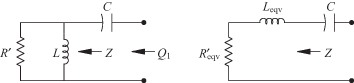
If the Q of the right-hand circuit is approximately that of the left-hand circuit in Fig. 3.12, then
(3.47)
![]()
The variable C represents the total capacitance of C1 and Cseqv in series as implied in Fig. 3.11 and represented in Fig. 3.12. For a high-Q circuit, circuit analysis gives the resonant frequency:
(3.48)
![]()
As a result, the approximate value for Q1 can be found:
(3.49)
![]()
Here Δf is the bandwidth in hertz and f0 is the resonant frequency.
3.8.4 Tapped C Design Procedure
The above ideas are summarized in Table 3.4, which provides a design procedure for the tapped C matching circuit. Similar expressions could be found for a tapped inductor transforming circuit, but such a circuit is typically less useful because high Q inductors are more difficult to obtain than capacitors.
TABLE 3.4 Tapped C Matching Circuit Design Formulas
| Step Number | Tapped C Formula |
| 1 | Q1 = f0/Δf |
| 2 | |
| 3 | |
| 4 | |
| 5 | C2 = Qp/ω0R2 |
| 6 | |
| 7 | C1 = CseqvC/(Cseqv − C) |
3.9 PARALLEL DOUBLE-TUNED TRANSFORMER
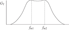
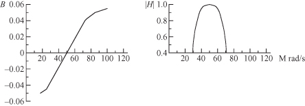
Each of the above described T, π, or tapped C matching circuits provide some control over the bandwidth. Where precise control over the bandwidth is required, a double-tuned circuit allows controlling bandwidth by specifying two different frequencies where maximum transmission occurs. For a small pass band, the midband dip in the transmission coefficient can be made small. Furthermore, the double-tuned circuit is especially useful when a large difference in impedance levels is desired, although its high end frequency range is limited. The filter transmission gain is shown in Fig. 3.13.
FIGURE 3.13 Double-tuned transformer response.
The double-tuned circuit consists of a coupled coil transformer with resonating capacitances on the primary and secondary side. This circuit is shown in Fig. 3.14. The transformer is described by its input and output inductance as well as the coupling coefficient k. The turns ratio for the transformer is
(3.50)
![]()
FIGURE 3.14 Real transformer with resonating capacitances.
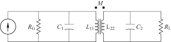
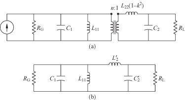
The circuit in Fig. 3.14 can be replaced by an equivalent circuit using an ideal transformer (Fig. 3.15a). Since an ideal transformer has no self-inductance, the inductances and coupling factor, k, must be added to the ideal transformer. The final circuit topology is shown in Fig. 3.15b). Looking toward the right through the ideal transformer, the circuit values in Fig. 3.15b) are
(3.51)
![]()
(3.52)
![]()
(3.53)
![]()
FIGURE 3.15 (a) Alternate equivalent circuit with ideal transformer and (b) final equivalent circuit.
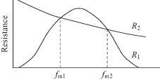
The circuit elements will be chosen to give an exact match at the two frequencies, fm1 and fm2. The circuit in Fig. 3.15b can be conceptually split into two (Fig. 3.16). The resistance R1 with the parallel resonant circuit will never be larger than RG. The right-hand side is an L matching circuit with the reactance of the shunt element monotonically decreasing with frequency. Hence, R2 monotonically decreases. Consequently, if RL is small enough, there will be two frequencies where R1 = R2. This is illustrated in Fig. 3.17.
FIGURE 3.16 Double-tuned circuit split into two.
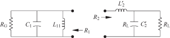
FIGURE 3.17 Plot of left- and right-hand resistance values vs. frequency.
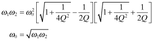
A design procedure for the parallel double-tuned circuit has been reviewed in [1] and is summarized below.The typical synthesis problem is to design a circuit that will match RG and RL over a bandwidth, Δf, at a center frequency, f0, with a given pass-band ripple. The bandwidth and center frequency are approximated by the following:
1. Determine fm1 and fm2 from Δf and f0:
(3.54)
![]()
(3.55)
![]()
The minimum pass-band gain for the filter is dependent on the difference between the match frequencies: The larger the distance between fm1 and fm2, the larger the dip in the center of the pass-band characteristic:
Equation (3.56) provides an approximation to the minimum gain at the center of the pass band, so that it predicts whether a chosen ripple factor can be met.
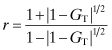
2. Determine the actual transducer gain for the given ripple factor:
(3.57)
![]()
3. Determine the resistance ratio r. If GT > GT,min, then the pass-band ripple specification can be met.
(3.58)
4. Calculate the Q2 at the two matching frequencies:
(3.59)
![]()
(3.60)
![]()
5.
Solve the following simultaneous equations for ![]() and
and ![]() :
:
(3.61)
![]()
(3.62)
![]()
6.
Find the value for ![]() :
:
(3.63)
![]()
7.
Calculate the input susceptance of the right-hand side where ![]() :
:
(3.64)
![]()
(3.65)
![]()
8. Solve the following simultaneous equations for L11 and C1:
(3.66)
![]()
(3.67)
![]()
9. Find the transformer coupling coefficient, and hence L22 and C2:
(3.68)
![]()
(3.69)
![]()
(3.70)
![]()
This procedure has been coded into the program DBLTUNE, and an example of its use is given in Appendix B.
The parallel double-tuned transformer makes use of a coupled coil. Sometimes coupled-coil transformers can be implemented in an integrated circuit with coupled spiral coils. This was referenced in Section 2.4.5 relative to using the ASITIC program.
3.10 CONCLUSIONS
This chapter has provided a variety of circuits that can be used to transform one impedance level to another. Impedance matching is required in many places within a transceiver, especially in the amplifiers. However, the circuit designs described in this chapter do not provide accurate bandwidth specifications, nor do they make use of transmission lines. These topics will be considered later in Chapters 5 and 6.
PROBLEMS
3.1. The graph in Fig. 3.18 shows the susceptance of a circuit as well as the frequency response.
a. From these graphs determine the Q of the circuit.
b. Determine the equivalent circuit that would approximate this frequency response. Give numerical values for the resistive and reactive components.
FIGURE 3.18 Susceptance and frequency response for Problem 3.1.
3.2. Design an impedance transforming network that matches a generator resistance, RG = 400 ![]() to a load resistance RL = 20
to a load resistance RL = 20 ![]() . The center frequency for the circuit is f0 = 6 MHz. The desired ripple (where appropriate) is to be less than 0.25 dB. In some cases, the ripple factor will not be able to be controlled in the design. The problem is to design four different transformation circuits with the above specifications, and for each design do an analysis using SPICE. See Appendix G, Sections G.1 and G.2.
. The center frequency for the circuit is f0 = 6 MHz. The desired ripple (where appropriate) is to be less than 0.25 dB. In some cases, the ripple factor will not be able to be controlled in the design. The problem is to design four different transformation circuits with the above specifications, and for each design do an analysis using SPICE. See Appendix G, Sections G.1 and G.2.
a. Design a two-element L matching circuit and check the results with SPICE.
b. Design a three-element tapped capacitor matching circuit with a bandwidth Δf = 50 kHz and check the results with SPICE to determine the actual bandwidth.
c. Design a three-element π matching circuit with a bandwidth of Δf = 50 kHz and check the results with SPICE to determine the actual bandwidth.
d. Design a double-tuned transformer matching circuit with a bandwidth of Δf = 50 kHz and check the results with SPICE to determine the actual bandwidth.
e. Repeat part (d) for a 3-dB bandwidth of 2 MHz. Again check the results using SPICE.
3.3. The π matching circuit shown in Fig. 3.4 is used to match the load, R = 1000 ![]() to R″ = 80
to R″ = 80 ![]() . If the intermediate resistance level is R′ = 20
. If the intermediate resistance level is R′ = 20 ![]() , determine the following:
, determine the following:
a. What is Q1?
b. What is Q2?
c. What is B1, the first susceptance nearest R?
d. What is the estimated 3-dB bandwidth for this circuit in terms of the center frequency, f0?
3.4. The tapped capacitor transformer is to be used in a narrow band of frequencies around ω = 4 × 10⁹ rad/s. In designing the matching circuit, the tapped C circuit is converted to an L matching circuit. If R2 in Fig. 3.10 is 50 ![]() , C2 = 8 pF, and C1 = 5.0 pF, then what is the total capacitance for the L matching circuit?
, C2 = 8 pF, and C1 = 5.0 pF, then what is the total capacitance for the L matching circuit?
3.5. A lossless π matching circuit has a load resistance R = 340 ![]() . The center frequency is ω0 = 20 × 106 rads/s and the bandwidth is Δω = 5 × 10⁶ rad/s. It is also known that the series element in the π circuit is L2 = 6 µH.
. The center frequency is ω0 = 20 × 106 rads/s and the bandwidth is Δω = 5 × 10⁶ rad/s. It is also known that the series element in the π circuit is L2 = 6 µH.
a. Determine the matching generator resistance that is smaller than the load.
b. Determine the susceptance at the load side.
c. Determine the susceptance at the generator side.
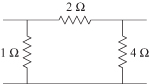
3.6. Determine the impedances that would match both sides of the two-port circuit in Fig. 3.19.
FIGURE 3.19 Circuit for Problem 3.6.
3.7. Show that the part of the circuit in Fig. 3.14 consisting of L11, L22, and M is equivalent to the part of the circuit in Fig. 3.15a consisting of L11, L22, n, and k. This can be done by equating corresponding z parameters of both circuits. Recall that k2 = k1k2, ![]() , and n = L11/M.
, and n = L11/M.
REFERENCE
1. P. L. D. Abrie, Design of RF and Microwave Amplifiers and Oscillators, Norwood, MA: Artech, 1999.