
APPENDIX F
Transistor and Amplifier
Formulas
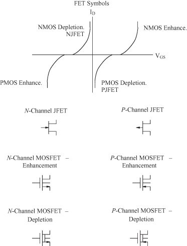
The following formulas are meant as a reminder of the fundamentals given in most standard electronics textbooks. Notation for the formulas have the traditional meanings. Depletion capacitances are all given with a negative sign in the denominator as in C = C0/(1 − V/ϕ)γ. Consequently, when the junction is reverse biased, the minus sign turns into a positive sign. Figure F.1 presents the basic FET features and symbols. The transistor body terminal typically is connected to the source or to ground. When the source is not grounded, the body effect modifies the transistor properties. The equations using the Early voltage, VA, should conform with the sign convention used by SPICE (VA > 0).
FIGURE F.1 FET symbols.
BIPOLAR TRANSISTOR PARAMETERS (BJT)
| Description | Formula |
| Collector current |
|
| Transconductance |
|
| Input resistance |
|
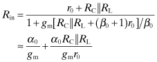
| Output resistance |
|
| Base charging capacitance | CD = τFgm |
| Emitter–base junction |
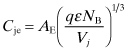
|
| Input capacitance | Cπ = Cb + Cje |
| Collector base |
|
| Collector substrate |
|
| Transition frequency |
|
| Thermal voltage |
|
JUNCTION FIELD-EFFECT TRANSISTOR PARAMETERS (JFET)
| Description | Formula |
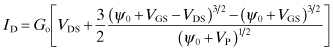
| Saturated drain current |
|
| VDS ≥ VGS − VP | |
| Ohmic region drain current |
|
| VDS < VGS − VP | |
|
|
|
|
|
|
| Transconductance |
|
| Output resistance |
|
| Gate–source capacitance |
|
| Gate–drain capacitance |
|
| Gate–substrate capacitance |
|
| n-Channel JFET | VP < 0 |
| p-Channel JFET | VP > 0 |
METAL–OXIDE SEMICONDUCTOR FIELD-EFFECT TRANSISTOR (MOSFET) PARAMETERS
| Description | Formula |
| Saturation region drain current |
|
| VDS ≥ VGS − Vt | |
| Ohmic region drain current |
|
| VDS < VGS − Vt | |
| Oxide capacitance |
|
| Transconductance |
|
| Output resistance |
|
| Input capacitance | Cin = CGS + CGD = CoxLW |
| Transition frequency |
|
| Surface mobility holes | μs = 200 cm2/V−s |
| Surface mobility electrons | μs = cm2/V−s |
| n-Channel JFET | p-Channel JFET |
| IDSS > 0 | IDSS < 0 |
| VP < 0 | VP > 0 |
|
|
|
|
|
|
| VP < VGS for |IDS| > 0 | VGS < VP for |IDS| > 0 |
| NMOS Enhancement | PMOS Enhancement |
| Vt > 0 | Vt < 0 |
| V GS > V t | V GS < V t |
|
|
|
| NMOS Depletion | PMOS Depletion |
| Vt < 0 | Vt > 0 |
| VGS > Vt < 0 for |IDS| > 0 | VGS < Vt for |IDS| |
|
|
|
SMALL-SIGNAL SINGLE-TRANSISTOR AMPLIFIER CONFIGURATIONS
| MOSFET | BJT |
| Common Source | Common Emitter |
| Rin = RB = R1 |
Rin = (rπ + rb) |
| Rout =
RD |
Rout =
Rc |
|
|
AV =
−gm (Rc |
| Source Degeneration | Emitter Degeneration |
| Rin =
RB = R1 |
Rin =
RB |
| ≈ rπ (1 + gmRE) | |
| Rout = ro[1 + (gm + gmb)RS] + RS | Rout =
RE |
| ≈ ro (1 + gmRE) | |
|
|
|
| Common Gate | Common Base |

|
|
| Rout =
RD |
|
| Gm = gm + gmb |
|
| AV = gm (RC|RL) | |
|
|
|
| Common Drain (Source Follower) | Common Collector (Emitter Follower) |
| Rin =
R1 |
Rin =
RB |
|
|
|
|
|