
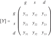
CHAPTER TEN
Oscillators and Harmonic Generators
10.1 OSCILLATOR FUNDAMENTALS
An oscillator is a circuit that converts energy from a power source (usually a dc power source) to ac energy. In order to produce a self-sustaining oscillation, there necessarily must be feedback from the output to the input, sufficient gain to overcome losses in the feedback path, and a resonator. There are a number of ways to classify oscillator circuits, one of those being the distinction between one-port and two-port oscillators. The one-port oscillator has a load and resonator with a negative resistance at the same port, while the two-port oscillator is loaded in some way at the two ports. In either case there must be a feedback path, although in the case of the one-port circuit this path might be internal to the device itself.
An amplifier with positive feedback is shown in Fig. 10.1. The output voltage of this amplifier is
![]()
which gives the closed-loop voltage gain
FIGURE 10.1 Circuit with positive feedback.
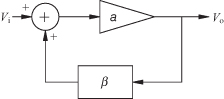
The positive feedback allows an increasing output voltage to feedback to the input side until the point is reached where
(10.2)
![]()
This is called the Barkhausen criterion for oscillation and is often described in terms of its magnitude and phase separately. Hence, oscillation can occur when |aβ| = 1 and ∠aβ = n × 360 °, where n is an integer. An alternate way of determining conditions for oscillation is determining when the value k < 1 for the stability circle as described in Chapter 8. Still a third way will be considered in Section 10.4.
10.2 FEEDBACK THEORY
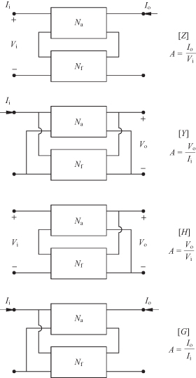
The active amplifier part and the passive feedback part of the oscillator can be considered as a pair of two two-port circuits. Usually the connection of these two port circuits occurs in four different ways: series–series, shunt–shunt, series–shunt, and shunt–series (Fig. 10.2). A linear analysis of the combination of these two two-port circuits begins by determining what type of connection exists between them. If, for example, they are connected in series–series, then the best way to describe each of the two-port circuits is in terms of their z parameters. The composite of the two two-port circuits is found by simply adding the z parameters of the two circuits together. Thus, if [za] and [zf] represent the amplifier and feedback circuits connected in series–series, then the composite circuit is described by [zc] = [za] + [zf]. The form of the feedback circuit itself can take a wide range of forms, but, being a linear circuit, it can always be reduced to a set of z, y, h, or g parameters any one of which can be represented by the symbol k for the present. The term that feeds back to the input of the amplifier is k12f. The k12f term, though small, is a significant part of the small incoming signal, so that it cannot be neglected. The open-loop gain, a, of the composite circuit is found by setting k12f = 0. Then using the normal circuit analysis, the open-loop gain is determined. The closed-loop gain is found by including k12f in the closed-loop gain given by Eq. (10.1). The Barkhausen criterion for oscillation is satisfied when ak12f = aβ = 1.
FIGURE 10.2 Four possible ways to connect the amplifier and feedback circuit. Composite circuit is obtained by adding designated two-port parameters. Units for “gain” are as shown.
10.3 TWO-PORT OSCILLATORS WITH EXTERNAL FEEDBACK
There are a wide variety of two-port oscillator circuits that can be designed. The variety of oscillators results from the different ways the feedback circuit is connected to the amplifier and the variety of feedback circuits themselves. Five of these shown in Fig. 10.3 are known as the Colpitts, Hartley, Clapp–Gouriet [1, 2], Armstrong, and Vackar [2, 3] oscillators. The Pierce oscillator is obtained by replacing the inductor in the Colpitts circuit with a crystal that acts like a high-Q inductor. As shown, the first four of these feedback circuits are drawn in a series–series connection while the Vackar is drawn as a series–shunt configuration. Of course, a wide variety of connections and feedback circuits are possible. In each of these oscillators, there is a relatively large amount of energy stored in the resonant reactive circuit. If not too much power is dissipated in the load, sustained oscillations are possible.
FIGURE 10.3 Oscillator types: (a) Colpitts, (b) Hartley, (c) Clapp–Gouriet, (d) Armstrong, and (e) Vackar.
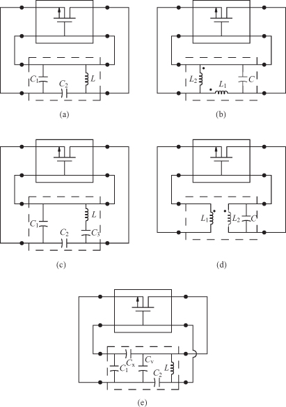
The Colpitts circuit is generally favored over that of the Hartley because the capacitors in the Colpitts circuit usually have higher Q than inductors at radio frequencies and come in a wider selection of types and sizes. In addition, the inductances in the Hartley circuit can provide a means to generate spurious frequencies because it is possible to resonate the inductors with parasitic device capacitances. Because the first element in the Colpitts circuit is a shunt capacitor, it is a low-pass circuit. For similar reasons, the Hartley oscillator is a high-pass circuit and the Clapp–Gouriet oscillator is a band-pass circuit. There is an improvement in the frequency stability of the tapped capacitor circuit over that of a single LC tuned circuit [1]. In a voltage-controlled oscillator application, it is often convenient to vary the capacitance to change the frequency. This can be done using a reverse-biased varactor diode as the capacitor. If the capacitance shown in Fig. 10.4a changes because of, say, a temperature shift, the frequency will change by
FIGURE 10.4 (a) Simple LC resonant circuit and (b) tapped capacitor LC circuit used in Colpitts oscillator.
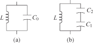
In the tapped circuit in Fig. 10.4b, C0 is the series combination of C1 and C2. Only C2 is used for tuning (Colpitts circuit), and it has a frequency stability given by
This has an improved stability by the factor of C0/C2. Furthermore, by increasing C0 so that C1 and C2 are increased by even more while adjusting the inductance to maintain the same resonant frequency, the stability can be further enhanced. The Clapp–Gouriet circuit exhibits even better stability than the Colpitts [2]. In this circuit, C1 and C2 are chosen to have large values compared to the tuning capacitor C3. The minimum transistor transconductance, gm, required for oscillation for the Clapp–Gouriet circuit increases ∝ ω3/Q. While the Q of a circuit often rises with frequency, it would not be sufficient to overcome the cubic change in frequency. For the Vackar circuit, the required minimum gm to maintain oscillation is ∝ ω/Q. This would tend to provide a slow drop in the amplitude of the oscillations as the frequency rises [2].
The oscillator is clearly a nonlinear circuit, but nonlinear circuits are difficult to treat analytically. In the interest of trying to get an approximate design solution, linear analysis is used. The circuit can be treated by small-signal linear mathematics to just prior to its breaking into oscillation. In going through the transition between oscillation and linear gain, the active part of the circuit does not change appreciably. As a justification for using linear analysis, the previous statement certainly has some flaws. Nevertheless, linear analysis does give remarkably close answers. More advanced computer modeling using methods such as harmonic balance will give more accurate results and in addition provide predictions of output power.
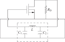
As an example, consider the Colpitts oscillator in Fig. 10.5. Rather than drawing it as shown in Fig. 10.3a as a series–series connection, it can be drawn in a shunt–shunt connection by simply rotating the feedback circuit 180 ° about its x axis. The y parameters for the feedback part are
(10.6)
![]()
FIGURE 10.5 Colpitts oscillator as shunt–shunt connection.
The equivalent circuit for the y parameters now may be combined with the equivalent circuit for the active device (Fig. 10.6). The open-loop gain, a, is found by setting y12f = 0:
(10.8)
![]()
FIGURE 10.6 Equivalent circuit of Colpitts oscillator.
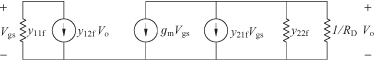
In the usual feedback amplifier theory the y21f term would be considered negligible since the forward gain of the feedback circuit would be very small compared to the amplifier gain. This is not assumed here. The open-loop gain, a, for the shunt–shunt configuration is
(10.9)
![]()
The negative sign introduced in getting ii is needed to make the current go north rather than south, as made necessary by the usual sign convention. Finally, using the Barkhausen criterion, oscillation occurs when βa = 1:
(10.10)
![]()
Making the appropriate substitutions from Eqs. (10.5) through (10.7) results in the following:
Both the real and imaginary parts of this equation must be equal on both sides. Since s = jω0 at the oscillation frequency, all even powers of s are real and all odd powers of s are imaginary. Since gm in Eq. (10.11) is associated with the real part of the equation, the imaginary part should be considered first:
(10.12)
![]()
Solution for the oscillation frequency is
(10.13)
![]()
Solving the real part of Eq. (10.11) with the now known value for ω0 gives the required value for gm:
The value for gm found in Eq. (10.14) is the minimum transconductance the transistor must have in order to produce oscillations. The small-signal analysis is sufficient to determine conditions for oscillation assuming the frequency of oscillation does not change with current amplitude in the active device. The large-signal nonlinear analysis would be required to determine the precise frequency of oscillation, the output power, the harmonic content of the oscillation, and the conditions for minimum noise.
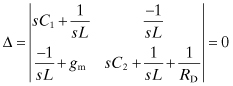
An alternative way of looking at this example involves simply writing down the node voltage circuit equations and solving them. The determinate for the two nodal equations is zero since there is no input signal:
(10.15)
This gives the same equation as Eq. (10.11) and, of course, the same solution. Solving nodal equations can become complicated when there are several amplifying stages involved or when the feedback circuit is complicated. Advanced theory for feedback amplifiers can be used in a wide variety of circuits.
10.4 PRACTICAL OSCILLATOR EXAMPLE
The oscillator shown in Fig. 10.7 is one of several possible versions of the Hartley circuit. In this circuit, the actual load resistance is RL = 50 ![]() . Directly loading the transistor with this size resistance would cause the circuit to cease oscillation. Hence, the transformer is used to provide an effective load to the transistor of
. Directly loading the transistor with this size resistance would cause the circuit to cease oscillation. Hence, the transformer is used to provide an effective load to the transistor of
(10.16)
![]()
and at the same time L2 acts as one of the inductors required by the Hartley circuit. By solving the network in Fig. 10.7b in the same way as described for the Colpitts oscillator, the frequency of oscillation and minimum transconductance can be found:
FIGURE 10.7 (a) Practical Hartley oscillator and (b) equivalent circuit.
For a 10-MHz oscillator biased with VDD = 10 V, the inductances L1 and L2 are chosen to be both equal to 1 μH. The capacitance from Eq. (10.17) is 126.6 pF. If the minimum device transconductance for a MOSFET is at least 0.333 mS, then R from Eq. (10.18) is 3000 ![]() . This transconductance is considerably smaller than is found in typical BJTs so that the minimum gm condition for oscillation is much easier to achieve with a BJT. For the resistance R to be 3000
. This transconductance is considerably smaller than is found in typical BJTs so that the minimum gm condition for oscillation is much easier to achieve with a BJT. For the resistance R to be 3000 ![]() , it will require the transformer turns ratio to be
, it will require the transformer turns ratio to be
![]()
and
![]()
These circuit values can be put into SPICE to check for the oscillation. However, SPICE will give zero output when there is zero input. Somehow, a transient must be used to start the circuit oscillating. If the circuit is designed correctly, oscillations will be self-sustaining after the initial transient. One way to initiate a start-up transient is to prevent SPICE from setting up the dc bias voltages prior to doing a time-domain analysis. This is done by using the UIC (use initial conditions) command in the transient statement. In addition it may be helpful to impose an initial voltage condition on a capacitance or initial current condition on an inductance. A second approach is to use the PWL (piecewise linear) transient voltage somewhere in the circuit to impose a short pulse at t = 0, which forever after is turned off. The first approach is illustrated in the SPICE net list for the Hartley oscillator:
Hartley Oscillator Example. 10 MHz, RL=50
L1 1 16 1uH
VDC 16 0 dc +.1
C 1 2 126.65pF
L2 3 2 1uh
L3 4 0 0.1667e−1u
K23 L2 L3 1.
RL 4 0 50.
MOS1 2 1 0 0 MOS-EX L=1.2um W=10um
VDD 3 0 10
.tran 1ns 2us uic
.op
* MOSIS CMOS 1.2um Level 1 version
.MODEL MOS-EX NMOS (LEVEL=1, PHI=0.6, TOX=2.12E−8,
+TPG=1 ,VTO=0.786, LD=1.647E−7,KP=9.6379E−5,
+U0=591.7,RSH=8.5450E1,GAMMA=0.5863,
+NSUB=2.747E16,
+CGDO=4.0241E−10,CGSO=4.0214E−10,
+CGBO=3.6144E−10,CJ=3.8541E−4,MJ=1.1854,CJSW=1.3940E−10,
+MJSW=0.125195,PB=0.8)
.END
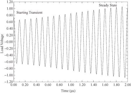
The result of the circuit analysis in Fig. 10.8 shows the oscillation building up to a steady-state output after many oscillation periods.
FIGURE 10.8 10-MHz Hartley oscillator time-domain response.
10.5 MINIMUM REQUIREMENTS OF THE REFLECTION COEFFICIENT
The two-port oscillator has two basic configurations: (1) a common source FET that uses an external resonator feedback from drain to gate and (2) a common gate FET that produces a negative resistance. In both of these the dc bias and the external circuit determine the oscillation conditions. When a load is connected to an oscillator circuit and the bias voltage is applied, noise in the circuit or start-up transients excites the resonator at a variety of frequencies. However, only the resonant frequency is supported and sent back to the device negative resistance. This in turn is amplified and the oscillation begins building up.
Negative resistance is merely a way of describing a power source. Ohm’s law says the resistance of a circuit is the ratio of the voltage applied to the current flowing out of the positive terminal of the voltage source. If the current flows back into the positive terminal of the voltage source, then, of course, it is attached to a negative resistance. The reflection coefficient of a load, ZL, attached to a lossless transmission line with characteristic impedance, Z0, is
Just like viewing yourself in the mirror, the wave reflected off a positive resistance load would be smaller than the incident wave. It is not expected that an image in the mirror would be brighter than the incident light. However, if the ![]() {ZL} < 0, then it would be possible for Γ in Eq. (10.19) to be greater than 1. The “mirror” is indeed capable of reflecting a brighter light than was incident on it. Negative resistance produces oscillations when the denominator of Eq. (10.19) approaches 0. The power needed to create the negative resistance must come from an external power source or bias supply.
{ZL} < 0, then it would be possible for Γ in Eq. (10.19) to be greater than 1. The “mirror” is indeed capable of reflecting a brighter light than was incident on it. Negative resistance produces oscillations when the denominator of Eq. (10.19) approaches 0. The power needed to create the negative resistance must come from an external power source or bias supply.
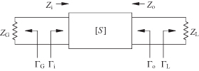
The conditions for oscillation then for the two-port circuit in Fig. 10.9 are
(10.20)
![]()
and
where k is the amplifier stability factor from Eq. (8.43) and Zi is the input impedance of the two-port circuit when it is terminated by ZL. The expression for oscillation in terms of reflection coefficients is easily found by first determining the expressions for Γi and ΓG:
(10.22)
![]()
FIGURE 10.9 Doubly terminated two-port circuit.
If ZG is now replaced by −Zi in Eq. (10.23),
Thus, Eqs. (10.21) and (10.24) are equivalent conditions for oscillation. In any case the stability factor, k, for the composite circuit with feedback must be less than 1 to make the circuit unstable and thus capable of oscillation.
An equivalent condition for the load port may be found from Eq. (10.24). From Eq. (8.17) in Chapter 8, the input reflection coefficient for a terminated two-port circuit was found to be
where Δ is the determinate of the S parameter matrix. Solving the right-hand side of Eq. (10.25) for ΓL gives
But from Eq. (8.18),
(10.27)
The last equality results from Eq. (10.26). The implication is that if the conditions for oscillation exists at one port, they also necessarily exist at the other port.
10.6 COMMON GATE (BASE) OSCILLATORS
A common gate configuration is often advantageous for oscillators because it has a large intrinsic reverse gain (S12g) that provides the necessary feedback. The subscript g, indicates common gate S parameters. Furthermore, feedback can be enhanced by putting some inductance between the gate and ground. Common gate oscillators often have low spectral purity but wide-band tunability. Consequently, they are often preferred in voltage controlled oscillator (VCO) designs. For a small signal approximate calculation, the scattering parameters of the transistor are typically found from measurements at a variety of bias current levels. Probably the S parameters associated with the largest output power as an amplifier would be those to be chosen for oscillator design. Since common source S parameters, Sij, are usually given, it is necessary to convert them to common gate S parameters, Sijg. Once this is done, the revised S parameters may be used in a direct fashion to check for conditions of oscillation.
The objective at this point is to determine the common gate S parameters with the possibility of having added gate inductance. These are derived from the common source S parameters. The procedure follows:
1. Convert the two-port common source S parameters to two-port common source y parameters (Appendix D).
2. Convert the two-port y parameters to three-port indefinite y parameters (Section 4.10).
3. Convert the three-port y parameters to three-port S parameters (Appendix D).
4. One of the three-port terminals is terminated with a load of known reflection coefficient, r.
5. With one port terminated, the S parameters are converted to two-port S parameters, which could be, among other things, common gate S parameters (Appendix E).
The first step, converting the S parameters to y parameters, can be done using the formulas in Table D.1 or Eq. (D.10) in Appendix D. For example, if the common source S parameters, [Ss], are given, the y parameter matrix is
where
(10.29)
![]()
Next the y parameters are converted to the 3 × 3 indefinite admittance matrix using the method given in [4] and Section 4.10. Purely for convenience, the third row and column will be added to the center of the matrix. Then the y11 will represent the gate admittance, the y22 the source admittance, and the y33 the drain admittance. The new elements for the indefinite matrix are then put in between the first and second rows and in between the first and second columns of Eq. (10.28). For example, the new y12 is
(10.30)
![]()
The values for y21, y23, and y32 are found similarly. The new y22 term is found from y22 = −y21 − y23. The indefinite admittance matrix is then represented as follows:
(10.31)
The S parameter matrix for 3 × 3 or higher order can be found from Eq. (D.9) in Appendix D:
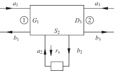
In this equation I is the identity matrix, while G and F are defined in Appendix D. When the reference characteristic impedances, Z0, are the same in all three ports, the F and the F−1 will cancel out. Determining S from Eq. (10.32) is straightforward but lengthy. At this point the common terminal is chosen. To illustrate the process, a common source connection is used in which the the source is terminated by a load with a reflection coefficient, rs, as shown in Fig. 10.10. If the source is grounded, the reflection coefficient is rs = −1. The relationship between the incident and reflected waves is
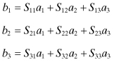
FIGURE 10.10 Three-port with source terminated with rs.
Solution for S11s is done by terminating the drain at port 3 with Z0 so that a3 = 0. The source is terminated with an impedance with reflection coefficient
or for any port
(10.35)
![]()
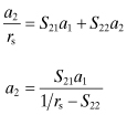
The reflection coefficient is determined relative to the reference impedance, which is the impedance looking back into the transistor. With Eq. (10.34), b2 can be eliminated in Eq. (10.33) giving a relationship between a1 and a2:
(10.36)
The ratio between b1 and a1 under these conditions is
(10.37)
![]()
This represents the revised S11s scattering parameter when the source is terminated with an impedance whose reflection coefficient is rs. In similar fashion the other parameters can be easily found as shown in Appendix E. The numbering system for the common source parameters is set up so that the input port (gate side) is port 1 and the output port (drain) is port 2. Therefore the subscripts of the common source parameters, Sijs, range from 1 to 2. In other words, after the source is terminated, there are only two ports, the input and output. These are written in terms of the three-port scattering parameters, Sij, which of course have subscripts that range from 1 to 3.
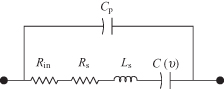
The common gate formulas are given in Appendix E. For a particular RF transistor, in which the generator is terminated with a 5-nH inductor, the required load impedance on the drain side to make the circuit oscillate is shown in Fig. 10.11 as obtained from the program SPARC (S parameters conversion). Since a passive resistance must be positive, the circuit is capable of oscillation only for those frequencies in which the resistance is above the 0-Ω line. An actual oscillator would still require a resonator to force the oscillator to provide power at a single frequency. A numerical calculation at 2 GHz that illustrates the process is found in Appendix E.
FIGURE 10.11 Plot of load impedance required for oscillation when generator side is terminated with 5-nH inductor.
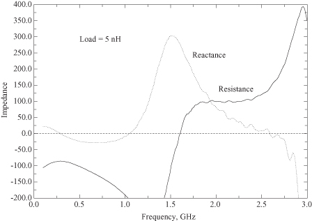
When the real part of the load impedance is less than the magnitude of the negative real part of the device impedance, then oscillations will occur at the frequency where there is resonance between the load and the device. For a one-port oscillator, the negative resistance is a result of feedback, but here the feedback is produced by the device itself rather than by an external path. Specific examples of one-port oscillators use a Gunn or IMPATT diode as the active device. These are normally used at frequencies above the frequency band of interest here. On the surface the one-port oscillator is, in principle, no different than a two-port oscillator whose opposite side is terminated in something that will produce negative resistance at the other end. The negative resistance in the device compensates for positive resistance in the resonator. Noise in the resonator port or a turn on transient starts the oscillation going. The oscillation frequency is determined by the resonant frequency of a high-Q circuit.
10.7 STABILITY OF AN OSCILLATOR
In the previous section, a method has been given to determine whether a circuit will oscillate or not. What is yet to be addressed is whether the oscillation will remain stable in the face of a small current transient in the active device. The simple equivalent circuit shown in Fig. 10.12 can be divided into the part with the active device and the passive part with the high-Q resonator. The current flowing through the circuit is
where A and ϕ are slowly varying functions of time. The part of the circuit with the active device is represented by Zd(A, ω) and the passive part by Z(ω). The condition for oscillation requires the sum of the impedances around the loop to be zero:
FIGURE 10.12 Oscillator model when passive impedance Z(ω) is separated from active device Zd(A, ω).
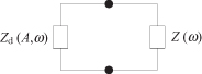
Ordinarily, the passive circuit selects the frequency of oscillation by means of a high-Q resonator. The relative variation of the impedance of the active device with frequency is small, so Eq. (10.39) can be approximated by
In phaser notation the current is
(10.41)
![]()
and
(10.42)
![]()
so that the voltage drop around the closed loop in Fig. 10.12 is
(10.43)
![]()
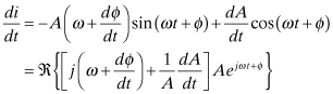
The time rate of change of the current is found by taking the derivative of Eq. (10.38):
(10.44)
Ordinarily, in ac circuit analysis, d/dt is equivalent to jω in the frequency domain. Now with variation in the amplitude and phase, the time derivative is equivalent to
(10.45)
![]()
The Taylor series expansion of Z(ω′) about ω0 is
(10.46)
![]()
Consequently, an expression for the voltage around the closed loop can be found:
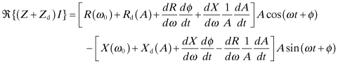
Multiplying Eq. (10.47) by cos(ωt + ϕ) and integrating will produce Eq. (10.48) by the orthogonality property of sine and cosine. Similarly, multiplying Eq. (10.47) by sin(ωt + ϕ) will produce Eq. (10.49):
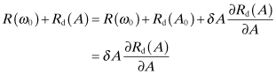
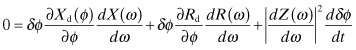
Multiplying Eq. (10.48) by dX/dω and Eq. (10.49) by dR/dω and adding will eliminate the dϕ/dt term. A similar procedure will eliminate dA/dt. The results are
Under steady-state conditions, the time derivatives are zero. Combination of Eqs. (10.50) and (10.51) gives
(10.52)
![]()
The only way for this equation to be satisfied is that it satisfies Eq. (10.40). However, suppose there is a small disturbance in the current amplitude of δA from the steady-state value of A0. Based on Eq. (10.40) the resistive and reactive components would become
The derivatives are, of course, assumed to be evaluated at A = A0. Substituting these into Eq. (10.50) gives the following differential equation with respect to time:
(10.55)
![]()
or
where
and
(10.58)
![]()
The solution of Eq. (10.56) is
![]()
which is stable if S > 0. The Kurokawa stability condition for small changes in the current amplitude occurs when Eq. (10.57) is positive [5]. As an example, consider the stability of a circuit whose passive circuit impedance changes with frequency as shown in Fig. 10.13 and device impedance that changes with current amplitude shown in the third quadrant of Fig. 10.13. As the current amplitude increases, Rd(A) and Xd(A) both increase:
![]()
![]()
FIGURE 10.13 Locus of points for oscillator passive and active impedances.
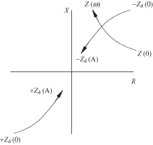
As frequency increases, the passive circuit resistance, R(ω), decreases and the circuit reactance, X(ω), increases:
![]()
![]()
From Eq. (10.57) this would provide stable oscillations at the point where Z(ω) and −Zd(A) intersect. If there is a small change in the current amplitude, the circuit tends to return back to the A0, ω0 oscillation point.
If there is a small perturbation in the current phase rather than the current amplitude, the stability criterion can be found in similar fashion as above. In this case the equations similar to (10.53) and (10.54) are
This is substituted into Eq. (10.51) in which the device impedance is given as a function of ϕ rather than A. The terms R(ω0) + Rd(ϕ) and X(ω0) + Xd(ϕ) are replaced by Eqs. (10.59) and (10.60), respectively:
(10.61)
(10.62)
![]()
where
and
(10.64)
![]()
Since
![]()
the oscillator is stable with respect to small changes in phase if S′ > 0.
10.8 INJECTION-LOCKED OSCILLATORS
A free-running oscillator frequency can be modified by applying an external frequency source to the oscillator. Such injection-locked oscillators can be used as high-power FM amplifiers when the circuit Q is sufficiently low to accommodate the frequency bandwidth of the signal. If the injection signal voltage, V(ωin), is at a frequency close to but not necessarily identical to the free-running frequency of the oscillator and is placed in series with the passive impedance, Z(ωin), in Fig. 10.12, then the loop voltage is
(10.65)
![]()
The amplitude of the current at the free-running point is A0 and the relative phase between the voltage and current is ϕ. Hence,
Up to this point, the passive impedance has been left rather general. As a specific example, the circuit can be considered to be a high-Q series resonant circuit determined by its inductance and capacitance together with some cavity losses, Rc, and a load resistance, RL:
(10.67)
![]()
Since ωin is close to the circuit free-running oscillator frequency ω0,
(10.68)
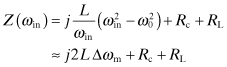
where Δωm = ω0 − ωin comes from the Taylor series expansion of Z(ωin).
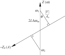
Equation (10.66) represented in Fig. 10.14 is a modification of that shown in Fig. 10.13 for the free-running oscillator case. If the magnitude of the injection voltage, V, remains constant, then the constant magnitude vector, |V|/A0, which must stay in contact with both the device and circuit impedance lines, will change its orientation as the injection frequency changes [thereby changing Z(ωin)]. However, there is a limit to how much the |V|/A0 vector can move because circuit and device impedances grow too far apart. In that case injection lock ceases. The example in Fig. 10.14 illustrates the simple series resonant cavity where the circuit resistance is independent of frequency. Furthermore, the |V|/A0 vector is drawn at the point of maximum frequency excursion from ω0. Here |V|/A0 is orthogonal to the Zd(A) line. If the frequency moves beyond ω1 or ω2, the oscillator loses lock with the injected signal. At the maximum locking frequency,
FIGURE 10.14 Injection-locked frequency range.
The expressions for the oscillator power delivered to the load, Po, the available injected power, and the external circuit Qext are
(10.70)
![]()
(10.71)
![]()
(10.72)
![]()
When these are substituted into Eq. (10.69) the well-known injection locking range is found [6]:
The total locking range is from ω0 − Δωm to ω0 + Δωm. The expression originally given by Adler [6] did not included the cos θ term. However, high-frequency devices often exhibit a phase delay of the RF current with respect to the voltage. This led to Eq. (10.73) where the device and circuit impedance lines are not necessarily orthogonal [7]. In the absence of information about the value of θ, a conservative approximation for the injection range can be made by choosing cos θ = 1. The frequency range over which the oscillator frequency can be pulled from its free-running frequency is proportional to the square root of the injected power and inversely proportional to the circuit Q as might be expected intuitively.
10.9 OSCILLATOR PHASE NOISE
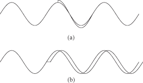
The fluctuations in the amplitude and especially the phase of an oscillator is an important limitation on the quality of an oscillator. In a receiver, the noise in the local oscillator of a mixer translates to noise in the intermediate frequency (IF) output. This implies the channel bandwidth must be larger than that required by the signal to accommodate the added phase noise. In a digital system using a clock, phase noise produces timing jitter. A noise current spike will primarily affect the amplitude of the oscillation if it occurs at one of the two extrema of the oscillation waveform. It will primarily affect the phase of the oscillation if it occurs during the zero crossing of the waveform (Fig. 10.15). When the noise fluctuation occurs at the waveform extrema in a stable oscillator, the amplitude will be quickly restored to its equilibrium value, and there will be no long-term effects. When the noise fluctuation occurs at the zero crossing, the phase change is permanent. Phase noise, ![]() {Δω}, is defined as the ratio of the noise power in a certain bandwidth (usually 1 Hz) at a certain offset frequency, Δω, away from the main carrier frequency to the signal power. The units for phase noise are typically given in dBc/Hz although the hertz part is inside the logarithm. This will be clarified later in this section.
{Δω}, is defined as the ratio of the noise power in a certain bandwidth (usually 1 Hz) at a certain offset frequency, Δω, away from the main carrier frequency to the signal power. The units for phase noise are typically given in dBc/Hz although the hertz part is inside the logarithm. This will be clarified later in this section.
FIGURE 10.15 Effect of noise (a) injected at peak and (b) at zero crossing.
The analysis of phase noise is done with a simple RLC resonator excited by an ideal negative resistance energy source (Fig. 10.16). A variety of models for phase noise have been proposed, but the linear time-varying theory developed by Hajimiri and Lee provides both a reasonably tractable and accurate model [8–10]. One of the assumptions they make is that a small increase in the input signal from a noise perturbation will produce a proportional output phase response. While the large-signal oscillator is clearly nonlinear, the small-signal perturbation is assumed to be linear. The second assumption is that the low-frequency 1/f noise can be folded up to the oscillator output band by the periodic and therefore time-varying signal.
FIGURE 10.16 Circuit model for phase noise calculation.
The linearity assumption allows defining an impulse response function that relates the input noise impulse to the output phase response. This is modeled as the unit step function, u(t), in the response function, hϕ. Since phase noise is much more important than amplitude noise, only the phase impulse response is useful:
(10.74)
![]()
Hajimiri [8] defines Γ(x) as the impulse sensitivity function. This function is periodic (though not necessarily sinusoidal) with a period equal to that of the oscillator. The maximum charge displacement on the tank capacitor, qmax, normalizes Γ(x) so that it is independent of signal level. This function is maximum at the signal zero crossings and zero at the extrema of the oscillation. Hajimiri [8] shows how values for this function might be obtained by simulation methods or approximate analytical methods for special cases. The phase response to a noise current is
Since Γ(x) is a periodic function, it can be expanded into a Fourier series:
Since θn represents the phase of the uncorrelated noise, it plays no significant role and is set to zero. The injected noise current, i(t), is represented as a sine wave at a multiple, m, of the oscillation frequency, ω0,
where ±Δω is the frequency offset above and below mω0 where there is “significant” noise. Equations (10.76) and (10.77) are substituted into Eq. (10.75). The orthogonality of the cosine functions demands that only the case where m = n survives. Also the product of the dc terms is dropped out for now in order to focus on the frequency terms:
(10.78)
![]()
From the trigonometric double-angle identity
(10.79)
![]()
(10.80)
It is assumed that Δω ![]() ω0 so that the first term is negligible. Also, the evaluation at t = −∞ is assumed to be zero. This shows two sideband offsets, ±Δω, of the phase spectrum around the oscillation frequency even if the noise is injected at some integer multiple, m, above ω0. As pointed out in [8, 10], the noise voltage and subsequently the noise power in the two sidebands are found using the phase-to-voltage converter:
ω0 so that the first term is negligible. Also, the evaluation at t = −∞ is assumed to be zero. This shows two sideband offsets, ±Δω, of the phase spectrum around the oscillation frequency even if the noise is injected at some integer multiple, m, above ω0. As pointed out in [8, 10], the noise voltage and subsequently the noise power in the two sidebands are found using the phase-to-voltage converter:
(10.82)
![]()
(10.83)
![]()
where Km is the prefix to sin Δωt in Eq. (10.81). Thus
(10.84)
![]()
(10.85)
![]()
Since for small argument sin(KmΔωt) ≈ Km sin(Δωt),
(10.86)
![]()
The ratio of the noise power in the sidebands at Δω to the carrier power is proportional to Km/2 or in log form:
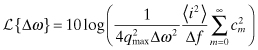
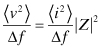
For white noise with a wide band of frequencies, all the Im in Eq. (10.87) are equal to each other, and the sum of the ![]() is 〈i2〉/Δf. This is the equivalent rms noise current. The total noise spectral density relative to the carrier is
is 〈i2〉/Δf. This is the equivalent rms noise current. The total noise spectral density relative to the carrier is
Experimentally, it is easier to find the rms value of Γ2 than the individual ![]() components. Parseval’s theorem gives the link between these:
components. Parseval’s theorem gives the link between these:
(10.89)
![]()
so that Eq. (10.88) is
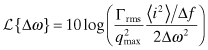
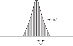
Equation (10.90) has two frequency terms: Δω is the offset frequency from the carrier where the noise is measured, and Δf is the band over which the noise is measured, typically 1 Hz. Figure 10.17 illustrates the distinction between Δω and Δf.
FIGURE 10.17 Phase noise over band of ±Δω within Δf.
The sideband power given in Eq. (10.90) represents first a translation of noise generated at mω0 to near dc by the Fourier coefficients. The 1/f noise is turned into 1/f2 noise near dc. This is a result of the implied integration of the impulse response function. The phase-to-voltage transformation upconverts the near dc 1/f2 noise back up to ω0. Thus, the oscillator will have both the original 1/f noise as well as a 1/f2 noise component. Minimization of the effects of noise implies using a high-Q resonator and a large signal. Also, the Γ(x) function should have a small value of Γdc so as to minimize upconversion of noise at low frequencies to ω0. Often the device has in itself a flicker noise component that is proportional to 1/f. When this is upconverted back up to ω0, the phase noise then also includes a 1/f3 frequency dependence as has been experimentally observed.
The Hajimiri model gives design insights on how noise might be minimized and provides a physical mechanism for observed phenomena. Its practical weakness lies in determining the impulse sensitivity function, Γ(x). Hajimiri [8] describes three methods for finding Γ that involve SPICE simulation or approximate analytical methods.
However, the assumption of linearity in an oscillator and the approximations that it brings is troublesome. The actual determination of Γ(x) is lengthy. The alternative would be a nonlinear model that would include both AM and PM as part of the noise generation mechanism. Still more general and accurate models have been developed such as that by Kaertner [11] and Demiri [12, 13]. While these two approaches give more accurate results, they do require simulation techniques to provide answers. Moreover, the increased rigor associated with these approaches has the effect of reducing the physical insight that the Hajimiri model has.
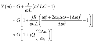
The phase noise models support oscillator insight and analysis. Practical design criteria are needed to actually make an oscillator. Optimization, however, requires using the simple linear time-invariant model. What is lost in accuracy is gained in finding an optimum design. The linear model assumes the existence of the parallel resonant tank circuit shown in Fig. 10.16. The tank admittance near resonance at ωo + Δω is
(10.91)
where R = 1/G. The magnitude squared of the impedance is, therefore,
The mean-square noise voltage per hertz is determined using Eq. (10.92):
(10.93)
(10.94)
![]()
(10.95)
![]()
The phase (noise-to-signal ratio) is
Zhu [14] started with this simple formula to arrive at a procedure for minimizing phase noise in an LC voltage-controlled oscillator. In integrated circuit design, the inductor takes up the major part of the real estate. Design of the oscillator is focused on controlling the inductor size. In the subsequent analysis the inductor area and the line spacing between turns is maintained constant, while the width and number of turns are varied to achieve various values of inductance.
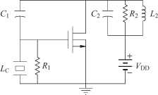
The focus here will be on the LC oscillator circuit in Fig. 10.18 since it provides lower phase noise than the popular ring oscillator. The LC oscillator is biased by a tail current source, IT. The tank circuit current waveform is a square wave that provides voltage harmonics. Only the fundamental of the voltage wave is supported so that its amplitude is ![]() . Since half of the current flows through the left side and half through the right side, this voltage is
. Since half of the current flows through the left side and half through the right side, this voltage is
(10.97)
![]()
FIGURE 10.18 The LC oscillator.
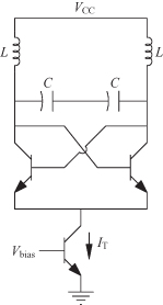
To emphasize that the G in Eq. (10.96) is the parallel tank circuit conductance, G is replaced by the symbol, gp. In terms of the tail current, IT, Eq. (10.96) is
(10.98)
![]()
The output waveform is proportional to the tail current, so, as expected, the phase noise decreases with increasing signal power. Similar calculations were carried out in [14] for noise resulting from the base spreading resistance and the shot noise of the transistor. In each case the phase noise was found to be proportional to ![]() . The tail current can be increased to the point where the oscillation signal becomes distorted. However, once this is set to a constant, it is not part of the design decisions. What remains for design analysis is minimizing
. The tail current can be increased to the point where the oscillation signal becomes distorted. However, once this is set to a constant, it is not part of the design decisions. What remains for design analysis is minimizing ![]() .
.
The analysis done in [14] was based on a fixed spiral inductor size of 400 × 400 µm2, which had a minimum conductor spacing of 2 µm. The line width was varied between 25 and 55 µm and the number of turns, n, varied from 2 to 5. The operating frequency was 900 MHz. Zhu’s [14] simulations show that by varying n and the line widths the optimum Q and ![]() occur at different values of L. As the inductance changes from 2 to 9 nH by varying n and line width, the maximum Q drops from 3.8 to 3.2, or 16%. At the same time, the
occur at different values of L. As the inductance changes from 2 to 9 nH by varying n and line width, the maximum Q drops from 3.8 to 3.2, or 16%. At the same time, the ![]() decreases 35.5%. Usually, it is thought that high Q(= 1/gpωoL) would imply small L to achieve low-phase noise. Zhu [14] has shown that large L gives lower phase noise. While increasing L2 does increase the noise, the gp decreases the noise even more. Furthermore, a comparison of two designs, one optimized for maximum Q and the other for minimum
decreases 35.5%. Usually, it is thought that high Q(= 1/gpωoL) would imply small L to achieve low-phase noise. Zhu [14] has shown that large L gives lower phase noise. While increasing L2 does increase the noise, the gp decreases the noise even more. Furthermore, a comparison of two designs, one optimized for maximum Q and the other for minimum ![]() showed that the latter had a 3.6-dB lower phase noise than the oscillator designed for maximum Q.
showed that the latter had a 3.6-dB lower phase noise than the oscillator designed for maximum Q.
10.10 HARMONIC GENERATORS
The previous sections have been concerned with fundamental frequency oscillators. It is also possible to use a highly stable low-frequency oscillator and use a frequency multiplier to obtain the desired radio frequency. The nonlinearity of a resistance in a diode can be used in mixers to produce a sum and difference of two input frequencies (see Chapter 11). If a large signal is applied to a diode, the nonlinear resistance can produce harmonics of the input voltage. However, the efficiency of the nonlinear resistance can be no greater than 1/n, where n is the order of the harmonic. However, a nonlinear susceptance (reciprocal of reactance) as found in a reverse-biased diode can provide efficient frequency upconversion:
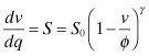
where ϕ is the built-in voltage and typically is between +0.5 and +1 V. The applied voltage v is considered positive when the diode is forward biased. The exponent γ for a varactor diode typically ranges from 0 for a step recovery diode to ![]() for a graded junction diode to
for a graded junction diode to ![]() for an abrupt junction diode. Using the nonlinear capacitance of a diode theoretically allows for generation of harmonics with an efficiency of 100% with a loss-free diode. This assertion is supported by the Manley–Rowe relations [15, 16], which describe the power balance when two frequencies, f1 and f2, along with their harmonics are present in a lossless circuit:
for an abrupt junction diode. Using the nonlinear capacitance of a diode theoretically allows for generation of harmonics with an efficiency of 100% with a loss-free diode. This assertion is supported by the Manley–Rowe relations [15, 16], which describe the power balance when two frequencies, f1 and f2, along with their harmonics are present in a lossless circuit:
(10.101)
![]()
These equations are basically an expression of the conservation of energy. From Eq. (10.100)
(10.102)
![]()
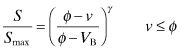
The depletion elastance given by Eq. (10.99) is valid for forward voltages up to about ![]() . Under forward bias, the diode will exhibit diffusion capacitance that tends to be more lossy in varactor diodes than the depletion capacitance associated with reverse-bias diodes. Notwithstanding, an analysis of harmonic generators will be based on Eq. (10.99) for all applied voltages up to v = ϕ. This is a reasonably good approximation when the minority carrier life time is long relative to the period of the oscillation. The maximum elastance (minimum capacitance) will occur at the reverse breakdown voltage, VB. The simplified model for the diode then is defined by two voltage ranges:
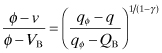
. Under forward bias, the diode will exhibit diffusion capacitance that tends to be more lossy in varactor diodes than the depletion capacitance associated with reverse-bias diodes. Notwithstanding, an analysis of harmonic generators will be based on Eq. (10.99) for all applied voltages up to v = ϕ. This is a reasonably good approximation when the minority carrier life time is long relative to the period of the oscillation. The maximum elastance (minimum capacitance) will occur at the reverse breakdown voltage, VB. The simplified model for the diode then is defined by two voltage ranges:
(10.103)
(10.104)
![]()
Integration of Eq. (10.99) gives
(10.105)
![]()
This can be evaluated at the breakdown point where v = VB and q = QB. Since VB and QB are negative quantities, their signs in Eq. (10.107) and following will be effectively reversed. Taking the ratio of this with Eq. (10.106) gives the voltage and charge relative to that at the breakdown point:
For the abrupt junction diode where ![]() , it is possible to produce power at mf1 when the input frequency is f1 except for m = 2 [17]. Higher order terms require that the circuit support intermediate frequencies called idlers. While the circuit allows energy storage at the idler frequencies, no external currents can flow at these idler frequencies. Thus, multiple lossless mixing can produce output power at mf1 with high efficiency when idler circuits are available.
, it is possible to produce power at mf1 when the input frequency is f1 except for m = 2 [17]. Higher order terms require that the circuit support intermediate frequencies called idlers. While the circuit allows energy storage at the idler frequencies, no external currents can flow at these idler frequencies. Thus, multiple lossless mixing can produce output power at mf1 with high efficiency when idler circuits are available.
Design of a varactor multiplier consists in predicting the input and output load impedances for maximum efficiency, the value of the efficiency, and the output power. A quantity called the drive, D, may be defined where qmax represents the maximum stored charge during the forward swing of the applied voltage:
(10.108)
![]()
If qmax = qϕ, then D = 1. An important quality factor for a varactor diode is the cutoff frequency. This is related to the series loss, Rs, in the diode:
(10.109)
![]()
When D ≥ 1, Smin = 0. When fc/(nf1) > 50, the tabulated values* given in [18] provide the necessary circuit parameters. These tables have been coded in the program MULTIPLY. The efficiency given by [18] assumes loss only in the diode where fout = mf1:
(10.110)
![]()
The output power at mf1 is found to be
(10.111)
![]()
The values of α and β are given in [17, 18]. If the varactor has a dc bias voltage, Vo, then the normalized voltage is
(10.112)
![]()
This value corresponds to the selected drive level. Finally, the input and load resistances are found from the tabulated values. The elastances at all supported harmonic frequencies up to and including m are also given. These values are useful for knowing how to reactively terminate the diode at the idler and output frequencies. A packaged diode will have package parasitic circuit elements as shown in Fig. 10.19 that must be considered in the design of a matching circuit. When given these package elements, the program MULTIPLY will find the appropriate matching impedances required external to the package. Following is an example run of MULTIPLY in the design of a 1–2–3–4 (idlers at each of these harmonics) varactor quadrupler with an output frequency of 2 GHz. The bold numbers are user input values:
Input frequency, GHz. =
0.5
Diode Parameters
Breakdown Voltage =
60
Built-in Potential phi =
0.5
Specify series resistance or cutoff frequency, Rs OR fc. <R/F>
f
Zero Bias cutoff frequency (GHz), fc =
50.
Junction capacitance at 0 volts (pF), Co =
0.5
Package capacitance (pF), Series inductance (nH) =
0.1, 0.2
For a Doubler Type A
For a 1–2–3 Tripler Type B
For a 1–2–4 Quadrupler Type C
For a 1–2–3–4 Quadrupler Type D
For a 1–2–4–5 Quintupler Type E
For a 1–2–4–6 Sextupler Type F
For a 1–2–4–8 Octupler Type G
For a 1–4 Quadrupler using a SRD, Type H
For a 1–6 Sextupler using a SRD, Type I
For a 1–8 Octupler using a SRD, Type J
Ctrl C to end
d
Type G for Graded junction (Gamma = .3333)
Type A Abrupt Junction (Gamma = .5)
Choose G or A
g
Drive is 1.0< D < 1.6.
Linear extrapolation done for D outside this range.
Choose drive.
2.0
Input Freq = 0.5000 GHz, Output Freq = 2.0000 GHz,
fc = 50.0000 GHz, Rs = 31.4878 Ohms.
Pout = 78.50312 mWatt, Efficiency = 75.47767%
At Drive 2.00, DC Bias Voltage = −7.76833
Harmonic elastance values
S0( 1) = 0.197844E+13
S0( 2) = 0.313252E+13
S0( 3) = 0.296765E+13
S0( 4) = 0.263791E+13
Total Capacitance with package cap.
CT0( 1) = 0.605450E−12
CT0( 2) = 0.419232E−12
CT0( 3) = 0.436967E−12
CT0( 4) = 0.479087E−12
Inside package, Rin = 643.400 RL = 346.470
Diode model Series Ls, Rin+Rs, S(v) shunted by Cp
Required impedances outside package.
Zin = 456.218 +j −606.069
Zout = 208.267 + j −242.991
Match these impedances with their complex conjugate
Match idler 2 with conjugate of 0 + j −379.181
Match idler 3 with conjugate of 0 + j −242.125
FIGURE 10.19 Intrinsic varactor diode with package.
PROBLEMS
10.1. Verify Eqs. (10.3) and (10.4).
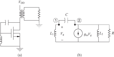
10.2. The crystal-controlled oscillator in Fig. 10.20 uses a tank circuit on the output side to achieve high effective reactance to help stabilize the oscillator. The narrow-band crystal is inductive when this circuit oscillates.
a. Write down the small-signal equivalent circuit for this oscillator.
b. Write down the equations needed to determine the frequency of oscillation and the minimum transistor gm oscillation to occur.
FIGURE 10.20 Crystal-controlled oscillator for Problem 10.2.
10.3. In Appendix D derive Eq. (D.9) from (D.10).
10.4. In Appendix E derive the common gate S parameters from the presumably known three-port S parameters.
10.5. Prove the stability factor S′ that is given in Eq. (10.63).
10.6. The measurements of a certain active device as a function of current give Zd (10 mA) = −20 + j30 ![]() and Zd (50 mA) = −10 + j15
and Zd (50 mA) = −10 + j15 ![]() . The passive circuit to which this is connected is measured at two frequencies: Z (800 MHz) = 12 − j10
. The passive circuit to which this is connected is measured at two frequencies: Z (800 MHz) = 12 − j10 ![]() and Z (1000 MHz) = 18 − j40
and Z (1000 MHz) = 18 − j40 ![]() . Determine whether the oscillator will be stable in the given ranges of frequency and current amplitude. Assume linear interpolation between the given values is justified.
. Determine whether the oscillator will be stable in the given ranges of frequency and current amplitude. Assume linear interpolation between the given values is justified.
Note
* Values taken, in part, from [18] are Copyright ©1965. AT&T. All rights reserved. Reprinted with permission.
REFERENCES
1. J. K. Clapp, “An Inductance-Capacitance Oscillator of Unusual Frequency Stability,” Proc. IRE, 36, pp. 356–358, March 1948.
2. J. K. Clapp, “Frequency Stable LC Oscillators,” Proc IRE, 42, pp. 1295–1300, Aug. 1954.
3. J. Vackar, “LC Oscillators and Their Frequency Stability,” Telsa Tech. Reports, Czechoslovakia, pp. 1–9, 1949.
4. W. K. Chen, Active Network and Feedback Amplifier Theory, New York: McGraw Hill, 1980.
5. K. Kurokawa, “Some Basic Characteristics of Broadband Negative Resistance Oscillator Circuits,” Bell Syst. Tech. J., 48, pp. 1937–1955, July–Aug. 1969.
6. R. Adler, “A Study of Locking Phenomena in Oscillators,” Proc. IRE., 22, pp. 351–357, June 1946.
7. K. Kurokawa, “Injection Locking of Microwave Solid-State Oscillators,” Proc IEEE, 61, pp. 1386–1410, Oct. 1973.
8. A. Hajimiri and T. H. Lee, “A General Theory of Phase Noise in Electrical Oscillators,” IEEE J. Solid-State Circuits, 33, pp. 179–194, Feb. 1998.
9. A. Hajimiri and T. H. Lee, “Corrections to ‘A General Theory of Phase Noise in Electrical Oscillators’,” IEEE J. Solid-State Circuits, 33, p. 928, June 1998.
10. T. H. Lee and A. Hajimiri, “Oscillator Phase Noise: A Tutorial,” IEEE J. Solid-State Circuits, 35, pp. 326–336, March 2000.
11. F. X. Kaertner, “Determination of the Correlation Spectrum of Oscillators with Low Noise,” IEEE Trans. Microwave Theory Tech., 37, pp. 90–101, Jan. 1989.
12. A. Demir, A. Mehrotra, and J. Roychowdhury, “Phase Noise in Oscillators: A Unifying Theory and Numerical Methods for Characterization,” IEEE Trans. Circuits Syst. I: Fund. Theory Appl., 47, pp. 655–674, May 2000.
13. A. Demir, “Phase Noise and Timing Jitter in Oscillators with Colored-Noise Sources,” IEEE Trans. Circuits Syst. I: Fund. Theory Appl., 49, pp. 1782–1791, Dec. 2002.
14. Z. Zhu, Low Phase Noise Voltage Controlled Oscillator Design, Ph.D. Dissertation, University of Texas at Arlington, Texas, 2005.
15. J. M. Manley and H. E. Rowe, “Some General Properties of Nonlinear Elements: Part I—General Energy Relations,” Proc. IRE, 44, July 1956, pp. 904–913.
16. H. E. Rowe, “Some General Properties of Nonlinear Elements: Part II—Small Signal Theory,” Proc. IRE, 46, pp. 850–860, May 1958.
17. M. Uenohara and J. W. Gewartowski, “Varactor Applications,” in H. A. Watson, ed., Microwave Semiconductor Devices and Their Circuit Applications, New York: McGraw-Hill, pp. 194–270, 1969.
18. C. B. Burckhardt, “Analysis of Varactor Frequency Multipliers for Arbitrary Capacitance Variation and Drive Level,” Bell Syst Tech. J, 44, pp. 675–692, April 1965.