Distortion in power amplifiers, Part V: output stages
From earlier work in this series, distortion from the small-signal stages may be kept to levels that will prove negligible compared with distortion from a closed-loop output stage. Similarly, future work in this series will show that distortion mechanisms 4 to 7 from my original list (EW + WW, July 93) can be effectively eliminated by lesser-known but straightforward methods. This leaves the third mechanism in its three components as the only distortion that is in any sense unavoidable: Class-B stages free from crossover artifacts are not exactly commonplace.
This is a good place to introduce the concept of a blameless amplifier, one designed so that all the easily-defeated distortion mechanisms have been rendered negligible. The word blameless has been carefully chosen to not imply perfection.
The first distortion, non-linearity in the input stage, cannot be totally eradicated but its onset can be pushed well above 20 kHz. The second distortion, non-linearity in the voltage amplifier stage, can be effectively eliminated by cascoding. Distortion mechanisms 4 to 7, concerned with such things as earth return loops, power supply impedance and non-linear loading, can be made negligible by simple measures to be described later.
Large-signal distortion
The large-signal nonlinearity performance of all the bipolar junction transistor stages outlined in the previous part of this series have these features in common:
Large-signal nonlinearity increases as load impedance decreases. In a typical output stage loaded with 8 Ω, closed-loop LSN is usually negligible, the THD residual being dominated by high-order crossover artefacts that are reduced less by negative feedback. At lower impedances, such as 4 Ω, relatively pure third harmonic becomes obvious in the residual.
LSN worsens as the driver emitter or collector resistances are reduced, because the driver current swings are larger. On the other hand, this reduction improves output device turn-off, and will so decrease switchoff distortion; the usual compromise is around 47–100 Ω.
The BJT output gain plots in the previous article reveal that the LSN is compressive, the voltage gain falling off with higher output currents. It is roughly symmetrical, generating third-harmonic, and is much greater at the very lowest load impedances; this is more of an issue now that 2 Ω-capable (for a few minutes, anyway) amplifiers are considered macho, and some speaker designers are happy with 2 Ω impedance troughs.
I suggest that the fundamental reason for this gain droop is the fall in output transistor beta as collector current increases, due to the onset of high level injection effects.1 In the emitter follower topology, this fall in beta draws more output transistor base current from the driver emitter, pulling its gain down further from unity; this is the change in gain that affects the overall transfer ratio.
The output device gain is not directly affected, as beta does not appear in the classical expression for emitter follower gain, providing the source impedance is negligibly low. This assertion has been verified by altering an output stage simulated in Spice such that the output bases are driven directly from zero impedance voltage sources rather than drivers; this abolishes the gain droop effect, so it must be in the drivers rather than the output transistors.
Further evidence for this view is that in Spice simulation, the output device Ebers-Moll model can be altered so that beta does not drop with Ic (simply increase the value of the parameter IKF) and once more the gain droop does not occur, even with drivers. Here is one of the best uses of circuit simulation tweaking the untweakable. Gain droop does not affect FET outputs, which have no equivalent beta loss mechanism. See Figure 12 of chapter 20, where the wings of the FET gain plot do not turn downwards at large outputs.
It used to be commonplace for output transistors to be sold in pairs roughly matched for beta, allegedly to minimise distortion; this practice seems to have been abandoned. Simulation shows that beta mismatch produces an unbalanced gain droop that markedly increases low order harmonics without much effect on the higher ones. Modern amplifiers with adequate feedback factors will linearise this effectively. This appears to be why the practice has ceased.
Improving large signal linearity
It will be suggested that, in a closed loop blameless amplifier, the large signal nonlinearity contribution to total distortion (for 8 Ω loading) is actually very small compared with that from crossover and switchoff. This is no longer true at 4 Ω and still less so for lower load impedances. Thus ways of reducing this mechanism will still be useful.
The best precaution is to choose the most linear output topology; The previous article suggested that the open loop complementary feedback pair output is at least twice as linear as its nearest competitor, (the emitter follower output) and so the CFP is usually the best choice unless the design emphasis is on minimising switchoff distortion.
In the small signal stages, we could virtually eliminate distortion. If the linearity of the input or voltage amplifier stage was inadequate, it was possible to come up with several ways in which it could be dramatically improved. A Class B output stage is a tougher proposition. In particular we must avoid complications to the forward path that lower the second amplifier pole P2, as this would reduce the amount of feedback that can be safely applied.
Several authors2,3 have tried to show that the output emitter resistors of bipolar outputs can be fine tuned in value to minimise large signal distortion, the rationale being that the current dependent internal re of the output transistors will tend to cause the gain to rise at high currents, and that this gain variation can be minimised by appropriate choice of the external Re. This is not true in practical output stages whose gain behaviour tends to be dominated by beta loss and its effect on the drivers. In any case the resistor values suggested are such tiny fractions of an ohm that quiescent stability would be perilous.
In real life the Re of a CFP output stage can be varied between 0.5 and 0.2 Ω without significantly affecting linearity; 0.22 Ω is a good compromise between efficiency and stability.
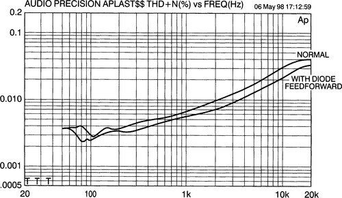
The gain droop at high Ics can be partly cancelled by a simple but effective feedforward mechanism. The emitter resistors Re are shunted with silicon power diodes, which with typical, circuit values will only conduct when 4 Ω loads (or less) are driven. This causes a slight gain increase that works against the beta loss droop. The modest but dependable improvement can be seen in Figure 1, measured with a 2.7 Ω load.
If a 100 W/8 Ω amplifier is required to drive 4 Ω loads then it will need paralleled output devices to cope with the power dissipation. Perhaps surprisingly, the paralleling of output BJTs (driven as usual from a single driver) has little effect on linearity, given elementary precautions to ensure current sharing. However, for the 2 Ω case there is a definite linearity improvement on resorting to tripled output devices; this is consistent with the theory that LSN results from beta loss at high collector currents.
Crossover distortion
The worst problem in Class B is the crossover region, where control of the output voltage must be transferred from one device to another. Crossover distortion generates unpleasant high order harmonics with the potential to increase in percentage as signal level falls. There is a consensus that crossover caused the transistor sound of the 1960’s, though to the best of my knowledge this has never actually been confirmed by the double blind testing of vintage equipment.
The Vbc -Ic characteristic of a bipolar transistor is initially exponential, blending into linear as the emitter resistance Re comes to dominate the transconductance. The usual Class B stage puts two of these curves back to back, and Peter Blomley has shown that these curves are non-conjugate,4 i.e. there is no way they can be rearranged to sum to a completely linear transfer characteristic, whatever the offset imposed by the bias voltage.
This can be demonstrated quickly and easily by Spice simulation; see Figure 2. There is at first sight not much you can do except maintain the bias voltage, and hence quiescent current, at some optimal level for minimum gain deviation at crossover; quiescent current control is a topic that could fill a book in itself, and cannot be considered properly here.

It should be said that the crossover distortion levels generated in a blameless amplifier can be low up to 1 kHz, being barely visible in residual noise and only measurable with a spectrum analyser. For example, if a blameless closed-loop Class B amplifier is driven through a TL072 unity gain buffer the added noise from this op-amp will usually submerge the 1 kHz crossover artifacts into the noise floor. (It is most important to note that distortion mechanisms 4 to 7 create disturbances of the THD residual at the zero crossing point that can be easily mistaken for crossover distortion, but the actual mechanisms are quite different.) However, the crossover distortion becomes obvious as the frequency increases, and the high order harmonics benefit less from NFB. See text panel Harmonic generation by crossover distortion (p. 197).
It will be seen later that in a blameless amplifier the linearity is dominated by crossover distortion, even with a well designed and optimally biased output stage. There is an obvious incentive to minimise it, but there seems no obvious way to reduce crossover gain deviations by tinkering with any of the relatively conventional stages considered so far. Significant improvement is only likely through application of one of the following techniques:
• The use of Class AB stages where the handover from one output device to the other is genuinely gradual, and not subject to the gm doubling effects that an over biased Class B stage shows. One possibility is the so called Harmonic AB mode.5
• Non-switching output stages where the output devices are clamped to prevent turn off, and thus hopefully avoiding the worst part of the Vbc -Ic curve.6
• Error correcting output stages implementing either error feedforward or error feedback. The latter is not the same thing as global NFB, being instead a form of cancellation.7
Once more, these will have to be examined in the future.
Switching distortion
This depends on several variables, notably the speed characteristics of the output devices and the output topology. Leaving aside the semiconductor physics and concentrating on the topology, the critical factor is whether or not the output stage can reverse bias the output device base emitter junctions to maximise the speed at which carriers are sucked out, so the device is turned off quickly.
The only conventional configuration that can reverse bias the output base emitter junctions is the emitter follower type II, described in the previous article. A second influence is the value of the driver emitter or collector resistors; the lower they are the faster the stored charge can be removed.
Applying these criteria can reduce HF distortion markedly, but it is equally important that it minimises output conduction overlap at high frequencies. If unchecked, overlap results in an inefficient and potentially destructive increase in supply current.8 Illustrating this, Figure 3 shows current consumption vs frequency for varying driver collector resistance, for a CFP type output.

Figure 4 shows how HF THD is reduced by adding a speed-up capacitor over the common driver resistor of a type II emitter follower. At LF the difference is small, but at 40 kHz THD is halved, indicating much cleaner switch-off. There is also a small benefit over the range 300 Hz to 8 kHz.

Selecting an output stage
Even if we stick to the most conventional of output stages, there are still an embarrassingly large number to choose from. The cost of a complementary pair of power fets is currently at least twice that of roughly equivalent BJTs, and taken with the poor linearity and low efficiency of these devices, the use of them may require a marketing rather than a technical motivation.
Turning to BJTs, and taking the material in this article with that in Part 4, I conclude that these are the following candidates for best output stage:
• The emitter follower type II output stage is the best at coping with switchoff distortion but the quiescent current stability is not of the best;
• The CFP topology has good quiescent stability and low LSN; its worst drawback is that reverse biasing the output bases for fast switchoff is impossible without additional HT rails;
• The quasi-complementary with Baxandall diode stage comes close to mimicking the emitter follower type stages in linearity, with a potential for cost saving on output devices. Quiescent stability is not as good as the CFP.
Closing the loop
In chapters 17 and 18, it was shown how relatively simple design rules could ensure that the THD of the small signal stages alone could be reduced to less than 0.001% across the audio band, in a repeatable fashion, and without using frightening amounts of negative feedback. Combining this subsystem with one of the more linear output stages such as the CFP version which gives 0.014% THD open loop, and having a feedback factor of at least 70 times across the band, it seems we have the ingredients for a virtually distortionless power amplifier, with THD below 0.001% from 10 Hz to 20 kHz. However, life is rarely so simple….
Table 1
Summary of closed loop amp THD performance
| 1 kHz (%) | 10 kHz (%) | ||
| Emitter follower | 0.0019 | 0.013 | Figure 5 |
| CFP | 0.0008 | 0.005 | Figure 6 |
| Quasi Bax | 0.0015 | 0.015 | Figure 7 |
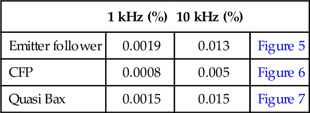
Figure 5 shows the distortion performance of such a closed loop amplifier with an emitter follower output stage, Figure 6 showing the same with a CFP output stage. Figure 7 shows the THD of a quasi-complementary stage with Baxandall diode.9 In each case distortion mechanisms 1, 2 and 4–7 have been eliminated by methods described in past and future chapters, to make the amplifier blameless.


It will be seen at once that these amplifiers are definitely not distortionless, though the performance is markedly superior to the usual run of hardware. THD in the LF region is very low, well below a noise floor of 0.0007%, and the usual rise below 100 Hz is very small indeed. However, above 2 kHz, THD rises with frequency at between 6 to 12 dB/octave, and the residual in this region is clearly time aligned with the crossover region, and consists of high order harmonics rather than second or third.
It is intriguing to note that the quasi-Bax output gives about the same HF THD as the emitter follower topology, confirming the statement that the addition of a Baxandall diode turns a conventional quasi-complementary stage with serious crossover asymmetry into a reasonable emulation of a complementary emitter follower stage.
There is significantly less HF THD with a CFP output; this cannot be due to large signal nonlinearity as this is negligible with an 8 Ω load for all three stages, and must result from lower levels of high order crossover products.
Despite the promising ingredients, a distortionless amplifier has failed to materialise, so we had better find out why?
When an amplifier with a frequency dependent NFB factor produces distortion, the reduction is not due to the NFB factor at the fundamental frequency, but the amount available at the frequency of the harmonic in question.
Harmonic generation by crossover distortion
The usual nonlinear distortions generate most of their unwanted energy in low order harmonics that NFB can deal with effectively. However, crossover and switching distortions that warp only a small part of the output swing tend to push energy into high order harmonics, and this important process is demonstrated here, by Fourier analysis of a Spice waveform.
Take a sinewave fundamental, and treat the distortion as an added error signal E, letting the ratio WR describe the proportion of the cycle where E > 0. If this error is a triangle wave extending over the whole cycle (WR = 1) this would represent large signal nonlinearity, and Figure 9 shows that most of the harmonic energy goes into the third and fifth harmonics; the even harmonics are all zero due to the symmetry of the waveform.
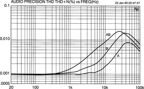

Figure 10 shows how the situation is made more like crossover or switching distortion by squeezing the triangular error into the centre of the cycle so that its value is zero elsewhere; now E > 0 for only half the cycle (denoted by WR = 0.5) and Figure 9 shows that the even harmonics are no longer absent. As WR is further decreased, the energy is pushed into higher order harmonics, the amplitude of the lower harmonics falling.
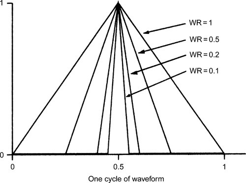
These high harmonics have roughly equal amplitude, spectrum analysis confirming that even in a blameless amplifier driven at 1 kHz, harmonics are freely generated from the 7th to the 19th at a level within a dB or so. The 19th harmonic is only 10 dB below the third.
Thus, in an amplifier with crossover distortion, the order of the harmonics will decrease as signal amplitude reduces, and WR increases; their lower frequencies allow them to be better corrected by the frequency dependant negative feedback. This effect seems to work against the commonly assumed rise of percentage crossover distortion as level is reduced.
A typical amplifier with open loop gain rolling off at 6 dB/octave will be half as effective at reducing fourth-harmonic distortion as it is at reducing the second harmonic. LSN is largely third (and possibly second) harmonic, and so NFB will deal with this effectively. However, both crossover and switchoff distortions generate high-order harmonics significant up to at least the 19th and these receive much less linearisation. As the fundamental moves up in frequency the harmonics do too, and get even less feedback. This is the reason for the differentiated look to many distortion residuals; higher harmonics are emphasised at the rate of 6 dB/octave.
Here is a real example of the inability of NFB to cure all amplifier ills. To reduce this HF distortion we must reduce the crossover gain deviations of the output stage before closing the loop. There seems no obvious way to do this by minor modifications to any of the conventional output stages; we can only optimise the quiescent current.
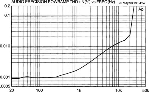
Increasing the quiescent current will do no good for, as outlined in the previous chapter, Class AB is generally Not A Good Thing, producing more distortion than Class B, not less. Figure 8 makes this painfully clear for the closed-loop case; Class AB clearly gives the worst performance. (As before, the AB quiescent was set for 50:50 m/s ratio of the gm doubling artifacts on the residual).
In this case the closed loop distortion is much greater than that from the small signal stages alone; however this is not automatic, and if the input pair is badly designed its HF distortion can easily exceed that caused by the output stage.
The distortion figures given in this article are rather better than the usual run. I must emphasise that these are not freakish or unrepeatable figures. They are simply the result of attending to all seven of the major sources of distortion rather than just one or two. I have so far built 12 CFP amplifiers, and performance shows little variation.
Conclusions
Taking this and the previous chapter together, we can summarise. Class AB is best avoided. Use pure Class A or B, as AB will always have more distortion than either. Fet outputs offer freedom from some BJT problems, but in general have poorer linearity, lower efficiency, and cost more.
Distortion generated by a blameless amplifier driving an 8 Ω load is almost entirely due to crossover effects and switching distortion. This does not hold for 4 Ω or lower loads where third harmonic on the residual shows the presence of large signal nonlinearity caused by beta loss at high output currents.