
4
Optical Sensors Based
on Photon Detection
Reinoud F. Wolffenbuttel
4.1 Introduction
Optical sensors are used for the measurement of radiation properties, such as intensity, polarization and spectral distribution (color when restricted to the visible spectral range). The two types of optical sensors available are: thermal detectors (=absorbing detectors) and photon detectors (=quantum detectors). The emphasis in this chapter is on silicon photon detectors, because of their high performance in applications in the visible spectral range and their compatibility with integrated circuit (IC) fabrication [1, 2].
A thermal detector is basically a tandem transducer in which the energy associated with the impinging radiation is first absorbed and the temperature rise due to the heat generated is measured, using one of the contact temperature sensors described in Chapter 7. The main advantage of the thermal detector is the spectral uniformity, which depends on the absorbing layer only. The photon detector enables the conversion of photons into electron–hole pairs, the concentration of which can be directly electrically measured.
Figure 4.1 shows the typical spectral response curves of a thermal detector (bolometer) and a silicon photon detector. The responsivity is basically the sensitivity specification. The spectral response of the thermal detector can be designed for wideband operation, since this property is determined by the absorber and can be engineered independently from the thermal measurement for constant spectral response over a wide spectral range. Ultimately, the spectral response uniformity is determined by interference at the protective window and results in a curve as shown in Figure 4.1(a). The main disadvantage of the thermal detector is the slow response due to thermal heat capacity of the detector.
The indirect type of band gap in silicon causes the absorption probability to increase from a minimum value at the indirect band gap (at EG = 1.12 eV) up to a maximum for photons carrying an energy that is sufficient to enable a direct transition from valence band to conduction band (at 3.4 eV, see next section). The silicon bandgap enables direct photon detection at photon energies in excess of the indirect bandgap, which is shown in Figure 4.1(b). Although the sensitivities of the thermal and photon detector are comparable (see Figure 4.1 at a 200Ω load), the actual figure of merit is the detection limit, which specifies the minimum optical signal level that can be reproducibly measured. When considering this parameter the photon detector demonstrates superior performance. A typical value of the detectivity of a silicon pn junction photon detector is D∗ = 1012 cm Hz1/2/W (see Section 4.6.2), which compares favorably to the thermal detector with D∗ = 108 cm Hz1/2/W. An additional advantage of the photon detector is its fast response.
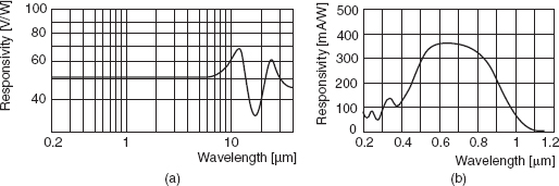
Figure 4.1 Typical spectral response of the: (a) thermal detector and (b) silicon pn junction photon detector
Operation of a photon detector is based on the capability of photons entering the semiconductor material to bring charge carriers into an excited state, provided that the photon carries sufficient energy to cross an available energy gap. The efficiency of the charge generation is usually expressed in terms of the internal quantum efficiency: η = number of charge carriers collected (i.e. measured) per photon entering the absorption volume [electrons/photon = dimensionless]. The external quantum efficiency also considers optical effects, such as reflection at the detector surface. Although the quantum efficiency is a convenient measure for describing photon detector sensitivity from the perspective of device physics, the responsivity, R [A/W], as used in Figure 4.1, is a more meaningful measure for specifying device performance from the viewpoint of the user. Nevertheless, these two parameters both specify detector sensitivity and are interchangeable. The range of typical values is: 0.3 < R < 0.5 A/W or 0.5 < η < 0.9.
The excess charge due to photon absorption of light of certain intensity yields a measurable electrical output. The most straightforward approach is the silicon intrinsic photon detector, in which the energy gap is the intrinsic bandgap of the semiconductor material. In a photoconductor the photogenerated excess charge results in a change in conductivity of a layer (see Section 4.4), whereas the charge is collected using a pn junction in a photodiode to yield an externally measurable photocurrent (see Section 4.5).
The energy associated with a photon of wavelength λ is equal to Eph = hPc/λ, where hP denotes Planck's constant and c the light propagation velocity in vacuum. This characteristic can be considered both an advantage and a limitation of any intrinsic photon detector. It enables the design of the photon detector for a strongly reduced sensitivity to background radiation, as compared to a thermal detector, by selecting a material with band gap energy much higher than the thermal energy of the background radiation: EG ![]() Eth,bg = kBTbg, with kB the Boltzmann constant and Tbg the background temperature. In case of ambient temperature Eth,bg = 1.38 × 10⁻²³ J/K × 300 K/(16 × 10−20 C) = 0.026 eV. The silicon indirect bandgap at EG = 1.12 eV enables photon detection not affected by background radiation, which is helpful in the detection of a low-intensity visible source [3, 4].
Eth,bg = kBTbg, with kB the Boltzmann constant and Tbg the background temperature. In case of ambient temperature Eth,bg = 1.38 × 10⁻²³ J/K × 300 K/(16 × 10−20 C) = 0.026 eV. The silicon indirect bandgap at EG = 1.12 eV enables photon detection not affected by background radiation, which is helpful in the detection of a low-intensity visible source [3, 4].
However, the same argument may also be interpreted as a fundamental limitation. In the intrinsic photon detector a cut-off wavelength results at: λmax = hPc/EG. In the case of silicon, λmax = 1110 nm. This wavelength-dependent spectral response makes application in the mid-infrared (mid-IR) spectral range impossible.
The alternative is an extrinsic photon detector, in which impurities are introduced to provide a donor or acceptor level within the band gap at such an energy level that electrons can be excited into the conduction band (or holes into the valence band) by photons carrying an energy equal to or in excess of the ionization energy, Ei, of that particular impurity used. Using phosphorus as the donor (or boron as the acceptor) yields Ei = 0.044 eV, hence: λmax = 28.3 μm. This property enables photon detection in the far-infrared spectral range, but has severe disadvantages. Firstly, the detector should be operated at liquid helium temperature to prevent the detector temperature from degrading noise performance. Secondly, this spectral range includes the peak blackbody emission of a background at room temperature, which results from Wien's displacement law as: λpk = cW/T = 2898 × 10−6 K m/300 K = 9.7 μm, where cW denotes the Wien constant [5]. Finally, the absorption coefficient, α, in an extrinsic detector depends on the dopant concentration used and is typically a factor of 103 lower than what can be achieved in an intrinsic detector.
Although dopant types are available that limit the spectral range to the mid-IR spectral range, extrinsic photon detection in silicon is rarely used and IR detection is generally based on thermal detectors (see Chapter 7) or on photon detection using special small band gap materials, such as PbS, PbSe, InAs, InSb, InGaAs or HgCdTe [3]. This chapter is restricted to the discussion of intrinsic photon detectors in silicon for use in the ultra-violet, visible and near-IR spectral ranges.
The process from impinging radiation to electrical response can be considered a sequence of effects:
(1) Light is incident on the detector surface.
(2) Light is transmitted through a coating into the silicon absorption volume.
(3) Photon absorption takes place with electron–hole pair generation.
(4) Excess charge is generated.
(5) Charge is converted into a measurable electrical output signal.
After a brief introduction of the key optical properties in silicon, the opto-electrical properties of silicon photon detectors are discussed in this sequence.
4.2 Photon Absorption in Silicon
The absorption of light in a silicon substrate is determined by the wavelength- dependent complex index of refraction, nSi∗(λ) = nSi(λ) − jkSi(λ) shown in Figure 4.2, with nSi as the index of refraction and kSi as the extinction coefficient. The absorption coefficient, α(λ), is as follows: α(λ) = 4πkSi(λ)/λ [6–11] and is shown in Figure 4.3.

Figure 4.2 Silicon index of refraction [11]
The strongly increasing extinction coefficient, kSi, for wavelengths below 380 nm (energy in excess of about 3 eV) is associated with a high value of the absorption coefficient and causes the material to strongly absorb UV light (metallic regime), whereas silicon behaves almost as a transparent material (dielectric) for wavelengths beyond 800 nm. Consequently, short-wavelength visible light penetrates only very shallowly into silicon and long-wavelength light penetrates much more deeply. Typically, a photon at 400 nm is absorbed within a layer of 0.1 μm thickness and a photon at 650 nm penetrates 100 μm into bulk silicon.
These optical properties of crystalline silicon are directly related to the silicon energy band structure shown in Figure 4.4 [10, 11]. The most characteristic feature in the energy momentum relation is the difference between the wave vectors at the highest energy state in the valence band, kv, as compared with the lowest energy state in the conduction band, kc. Such a band diagram is typical for an indirect bandgap material, such as germanium and silicon. The wave vectors kv and kc define the momentum of electron in the valence band or conduction band respectively (P = hPk/(2π)). The indirect bandgap energy is at EG = 1.12 eV and a direct transition is possible in the case where a photon with energy equal to 3.4 eV is absorbed. In silicon kv ≈ 0 and kc = 0.85(π/aSi), where π/aSi denotes the first Brillouin zone edge, with aSi = 0.543 nm the silicon lattice constant.

Figure 4.3 Silicon intrinsic absorption coefficient [11]

Figure 4.4 Simplified silicon band gap diagram
Incident photons carrying an energy that exceeds the bandgap are in principle able to excite electrons from valence to conduction band, provided that momentum is simultaneously also preserved. In case the photon carries exactly the indirect bandgap energy, EG = 1.12 eV, a wave vector should be supplied equal to: Δk = kc − kv = 0.85(π/aSi) = 4.9 × 10⁹ m−1. A photon at 1.12 eV (λ = hPc/Eg = 1110 nm) supplies a wave vector equal to: kph = 2π/λ = 5.7 × 10⁶ m−1, which is highly insufficient. Therefore, the wave vector that is required at a given photon energy to conserve both energy and momentum, and thus to enable an electron transition, must be supplied by the lattice. Basically, a phonon with the proper amount of momentum should be consumed. The amount of momentum required decreases with surplus photon energy (ΔE = hPν − Eg + Eph), where Eph is the energy released by the consumption of a photon. The different photon modes, the band curvatures at the extremes of the valence band (heavy and light holes) and the conduction band yield an absorption coefficient, α(λ), proportional to (hPν − Eg + Eph)3/2/(hPν)3 [10, 11], which should also be considered.
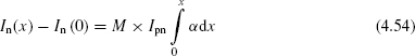
The photon flux in an absorption volume decreases with penetration depth x according to:
where Φto is the flux entering the absorption volume at the coating–silicon interface, as shown in Figure 4.5. Since each photon absorbed generates η electron–hole pairs, the amount of charge generated per unit time at depth x is proportional to the local rate of absorption (i.e. the decrease in flux at depth x): dQ(x)/dt = −qηdΦ(x)/dx = αΦ(x). Assuming the extreme case of photon flux of one monochromatic wavelength Φto(λ), with absorption and photocharge collection restricted to a layer between the surface at x = 0 and a boundary at x = d results in a photocurrent:

Figure 4.5 Light transmission into a silicon detector with electron-hole pair generation at absorption

where q is the unit charge. Obviously, α(λ), results in a wavelength dependence in case of nonzero exp(−α(λ)d) (i.e. when α(λ)d is smaller than about 3). Usually the wavelength-dependent spectral response is described in terms of the photon absorption rate Nλ (number of photons at wavelength λ absorbed per unit time) and detector gain, G:
In Equation (4.2) gain G = 1 and Nλ = Φto(λ)(1−exp(−α(λ)d). The total photocurrent generation results from integration over the entire spectrum of the incident light. The efficiency of the photocharge collection over a well-defined absorption volume and any gain therein is highly specific for the photon detector considered and is discussed in Sections 4.4–4.6. In Equation (4.2) the case for photon flux entering the silicon after transmission and reflection of incident light at the air–detector interface is considered. This introduces another wavelength dependence, which is discussed in the next section.
4.3 The Interface: Photon Transmission Into Silicon
The polished front surface of silicon prime wafers is of high optical quality. However, processing introduces surface roughness and scattering. Moreover, a direct silicon–air interface is not available. Exposure of a bare wafer to ambient air already introduces a silicon oxide layer of several nanometers thickness. IC processing introduces films of such thickness that interference effects are introduced. These optical effects at the air–silicon interface need to be considered in the calculation of the transmission of incident light through the coating into the bulk silicon and for the overall response of a photon detector. Without optical coating, the reflection, R(λ), at the air–silicon interface is governed by Snell's law and is expressed for normal incidence as [12] :
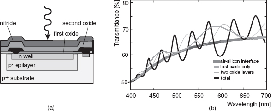
Figure 4.6 Light transmission into silicon in case of CMOS processing with several oxide layers and a nitride film on top
At λ = 450 nm, nSi = 4.8 and kSi = 0.3 (Figure 4.2), reflection R(λ) = 44 % and transmission T(λ) = 56 %. The transmission at the direct air–silicon interface is represented by the monotonic lower curve in Figure 4.6(b). Transmission is low, basically because of the large difference between the air and the silicon index of refraction.
A general technique for improving performance is based on the deposition of a thin film with an index of refraction in between those of air and silicon. In principle this approach is very compatible with the technology used for the fabrication of practical devices in silicon, which usually involves the application of oxides and nitrides for masking and surface passivation. A CMOS process typically involves the deposition of several silicon oxide (SiO2) layers plus a subsequent silicon nitride (Si3N4) layer and results in a vertical device structure, which is shown schematically in Figure 4.6(a) [1, 2].
Note that the vertical scale in Figure 4.6(a) is nonlinear. The substrate thickness exceeds 500 μm, whereas the total thickness of the stacked top layers is limited to about 5 μm. The thin-film coating does introduce interference effects, which is demonstrated by the curves in Figure 4.6(b). When using IC technology, the thickness of an oxide or nitride coating of the silicon photon detectors is sufficient to significantly affect the reflection of light in the near-IR, visible and UV parts of the spectrum [11]. In the relatively simple case of a silicon detector coated with an oxide layer, the transmission coefficient T(λ) from air through this silicon oxide layer of thickness dox into bulk silicon can analytically be derived as [12]:

where nox denotes the refraction index of the silicon oxide layer (nox = 1.46), nSi*(λ) = nSi(λ) − jkSi(λ) the silicon complex index of refraction and δ = 2πnoxdox/λ the phase change per traversal through the oxide film. In case of oxide coating only, the index of refraction increases monotonically along the path of the impinging light and transmission is improved over the entire spectrum (gray curves in Figure 4.6(b)). Interference between transmitted light and light reflected at the oxide–silicon interface results in a wavelength-dependent transmission. Increasing the silicon oxide layer thickness increases the number of interference peaks within a given spectral band.
The transmission of light through an air–nitride–oxide–silicon structure at normal incidence is generally calculated numerically using the multiplication of the matrices that describe the reflection and transmission at each of the specific layers [13, 14]. The index of refraction of the nitride is greater than that of the oxide. Hence, the transmission at destructive interference can be improved using a silicon nitride thin film in between the silicon dioxide top film and the silicon wafer.
When including the wavelength dependence of the transmission through the detector coating, Equation (4.3) can be rewritten as:
where gain G = 1 and Nλ = Φi(λ)(1 − exp(−α(λ)d) and external quantum efficiency ηext(λ) = η(λ)(1 − R(λ)). This expression directly relates the detector response to the spectrum of the incident light.
The type of surface passivation layer is not restricted to thermal silicon oxide. Fabrication-compatible materials routinely used in standard microelectronic processing in silicon are: crystalline Si, thermally grown SiO2, LPCVD polysilicon, amorphous silicon, silicon nitride (low-stress and stoichiometric), oxides (LTO, PSG, BSG, BPSG), PECVD oxynitrides and thin-film metals [11, 15]. Reliable optical data on crystalline silicon are available. However, the optical characterization of thin films is often strongly depending on the details of the deposition technology. Generally, thin films demonstrate a higher value of the extinction coefficient (i.e. higher absorption) especially in the blue–UV spectral range. In many applications, integrated detectors are covered with a thin conducting polysilicon layer (e.g. to be used as control gate). The optical properties of polysilicon in the visible part of the spectrum are similar, but not equal, to those of crystalline silicon, as is shown in Figure 4.7.
It is important to note that the two polysilicon layers have very different characteristics. The lower polysilicon film is characterized by optical properties closer to those of crystalline silicon, which is due to subsequent layer deposition and anneal steps. The larger thermal budget accumulated by the lower polysilicon film is mainly due to the influence of the deposition and the in situ anneal required to realize the second polysilicon layer. The intermediate SiO2 layers are usually PECVD-deposited at about 350 °C, so that the influence of their deposition on the total thermal budget can be neglected. Consequently, the structure of the lower polysilicon layer is recrystallized to a larger extent than that of the upper, i.e. more amorphous, polysilicon film. Hence, the optical characteristics are very sensitive to subsequent processing and significant differences between IC processes.
Dedicated software for analyzing optical properties is available and can be used either to minimize spectral dependence (antireflective coating) or to design for a specified spectral response of the photon detector [16, 17]. The intention of this section was to demonstrate that the accuracy of such a tool depends markedly on the material database and should incorporate the details in the actual processing.

Figure 4.7 Wavelength dependence and process dependence of the index of refraction of polysilicon, with n∗= n – jk [11]
Thin-film metal layers are used in silicon photon detectors, despite the high absorption. The reflectance of some frequently used metals in silicon photon detectors are shown in Figure 4.8 [18, 19]. Although gold is generally the material of choice for high reflectivity in the visible and infrared spectral range, aluminum is more suitable in multilayer interference filters for selective UV light detection, based on a stack of alternating silicon oxide and aluminum films [20]. Another application is in Fabry–Perot interferometers, where thin silver and aluminum layers are used for the realization of a mirror on either side of a deposited dielectric layer [21].
4.4 Photon Detection in Silicon Photoconductors
Photon detection involves the direct conversion of photons into electron–hole pairs upon absorption and measurement of the electrical signal. Devices primarily differ in the way these excess electron–hole pairs result in a measurable change in an electrical quantity. Usually a classification into two groups of photon detectors is used. The first is the photoconductor, where excess charge is measured by means of the electrical conductance of the layer in which absorption has taken place. The second is the pn junction-type of photon detector, in which electron–hole pairs are separated and collected using the electric field caused by space charges at the pn junction. This device is usually referred to as the photodiode or solar cell depending on the mode of operation (current readout for intensity measurement or the photovoltaic mode for opto-electrical power conversion respectively).

Figure 4.8 Reflectance of some of the metals used in silicon photon detectors
The basic pn junction photon detector has a limited detectivity, which is discussed in Section 4.6. Modifications, such as the phototransistor, the avalanche photodiode and the photo-capacitance, possess the ability to provide gain and hence have the potential to improve detectivity. These are discussed separately in Section 4.7.
The mathematical description of both the photoconductor and the pn-junction photon detector operation is essentially similar and involves solving the continuity equation and the insertion of the result in the definitions for electron current density, Jn, and hole current density, Jp. Assuming a one-dimensional device with parameter x the depth into the silicon:

with μn the electron mobility, n(x) the electron concentration at depth x, Dn the electron diffusion coefficient, μp the hole mobility, p(x) the hole concentration at depth x and Dp the hole diffusion coefficient (the Einstein relation applies: D/μ = kBT/q).
In the case that no charge is stored in the system (e.g. no depletion layer), the total current density, Jtotal = Jn(x) + Jp(x), can be assumed to be constant irrespective of x (the charge neutrality assumption). These expressions indicate a drift current due to an internal electric field, E(x), and a diffusion current due to a gradient in carrier concentration. In the case of a single homogenously doped layer with ohmic contacts at either side and no significant charge generation or charge recombination mechanism, the diffusion term can be disregarded and Ohm's law remains: Jtotal/E = q(μnn + μpp). An n-type layer of uniform doping concentration ND results in: n = ND and p = (ni2/ND) ![]() ND, with ni2 as the material and temperature dependent intrinsic carrier concentration. Hence: Jtotal/E ≈ qμnND. Similarly, a p-type layer of uniform doping concentration NA results in: Jtotal/E ≈ qμpNA.
ND, with ni2 as the material and temperature dependent intrinsic carrier concentration. Hence: Jtotal/E ≈ qμnND. Similarly, a p-type layer of uniform doping concentration NA results in: Jtotal/E ≈ qμpNA.
In a photoconductor charge is generated by incident photons. The resulting distributions of the carrier concentrations in the case of generation rate G and recombination rate R are described by the continuity equations. Inserting the current density equations yields:

where μn denotes the electron mobility and μp is the hole mobility. In the steady-state situation, ∂n(x)/∂t = ∂p(x)/∂t = 0. Solving this equation provides n(x) and p(x) which can subsequently be used to predict the device characteristics.
The mathematical description of the pn-junction-based photon detector is more complicated, since the presence of a junction space charge region implies that both drift and diffusion currents need to be considered. However, the basic approach remains the same and is discussed in Section 4.5. The differences are in the presence of a significant electric field and in the boundary conditions.
4.4.1 Photoconductors in Silicon: Operation and Static Performance
The photoconductor is essentially a slab of silicon of certain nominal resistivity as defined by doping. Photogenerated excess charge carriers add to the carrier concentration and, hence, modulate the resistivity. The resulting change in resistance can be externally measured using the current, Idet, drawn from a fixed-value voltage source, Vexc.
Analytical expressions can be derived when assuming a one-dimensional problem (no lateral gradients in excess charge generation). Consider a photon flux Φto [photons m−2 s−1] of wavelength λ entering an n-type silicon absorbing layer of constant doping concentration ND at the surface (x = 0), as shown in Figure 4.9. As discussed in Section 4.2, silicon is characterized by a wavelength-dependent absorption coefficient, α(λ), and the photon flux at depth x is described by: Φ(x) = Φto exp(−α (λ) x). In the following the wavelength dependence is not explicitly mentioned (i.e. α(λ) = α).
The generation rate at depth x results in: G(x) = −dΦ(x)/dx = αΦ(x) [electron–hole pairs m−3 s−1]. Photon absorption therefore results in excess charge at the actual absorption depth. Equilibrium is restored by recombination and diffusion of these excess charge carriers. The recombination rate of excess charge carriers is expressed as: R(x) = Δn(x)/τ = (n(x) − ND)/τn, where Δn(x) denotes the excess charge concentration at depth x and τn the excess carrier lifetime.
In the particular device depicted in Figure 4.9, Vexc is assumed small enough to disregard the effect of the electric field (E(x) = 0 and ∂E(x)/∂x = 0). Diffusion is assumed to take place in the x-direction only. An imbalance between the electron concentration at depth x (= n(x)) and depth x + dx (= n(x + dx) results in diffusion described by Fick's (second) law of diffusion: dn(x)/dt = Dnd2n(x)/dx2, with Dn [m2 s−1] as the electron diffusion coefficient. Similar considerations apply to the excess hole concentration and yield the continuity equations:

Figure 4.9 Schematic structure of the basic photoconducto

This set of second-order differential equations can, in principle, be solved analytically. It is generally true that the minority carrier lifetime is much shorter than the majority carrier lifetime. In a p-type photoconductor, such as the vertical device shown in Figure 4.10(a), τn ![]() τp and only the continuity equation for holes needs to be considered. Alternatively, the continuity equation for electrons applies to the lateral photoconductor in the n-layer (n-well in CMOS), which is shown schematically in Figure 4.10(b). Operation of the photoconductor is, therefore, defined by majority charge carriers.
τp and only the continuity equation for holes needs to be considered. Alternatively, the continuity equation for electrons applies to the lateral photoconductor in the n-layer (n-well in CMOS), which is shown schematically in Figure 4.10(b). Operation of the photoconductor is, therefore, defined by majority charge carriers.
The solution of the continuity equation depends on the boundary condition imposed by the actual device structure. In the case that the entire volume of p-silicon is used (p− epilayer plus p+ bulk in Figure 4.10(a)), the excess charge density at the top and bottom surfaces are set by the respective surface recombination velocities St and Sb(p(0) = (Dp/St) × (dp/dt)|x=0 and p(b1) = −(Dp/Sb) × (dp/dt)|x=b1). This p-type vertical detector is characterized by electrodes on the front and backside surfaces. The voltage, Uexc, is connected between the NMOS drain/source layer (SP) and the backside contact and results in a current flow in the same direction as the photo-excitation. The disadvantage of this approach is the electrodes. A transparent top electrode is required. This can be achieved using a special material, such as indium tin oxide (ITO). An alternative is to use a shallow layer of very high p-type concentration. Contacting the bottom electrode remains poorly compatible with the kind of planar processing that is commonplace in IC fabrication.
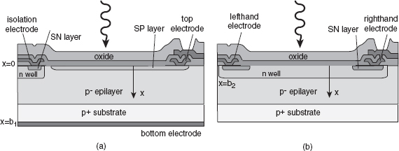
Figure 4.10 Schematic cross-sectional view of: (a) the vertical and (b) the lateral CMOS-compatible p-type photoconductor
The n-type lateral photoconductor shown in Figure 4.10(b) is a more IC-compatible structure and uses an n-type layer of doping concentration ND in the p− epilayer, which is of doping concentration NA. The lateral photoconductor has the electrodes at the sides of the element and is electrically contacted using the PMOS drain/source layer (SN). The lateral current flow is normal to the photo-excitation direction, which ensures efficient lateral removal of excess charge. Hence, any vertical charge transport is minimized (d2n(x)/dx2 = 0) and the diffusion term in Equation (4.7) can be disregarded.
The boundary condition for the top surface of the lateral photoconductor is similar to that of the vertical device (n(0) = (Dn/St) × (dn/dt)|x = 0), but the electron concentration at the lower boundary is determined by the depletion layer due to the pn-junction and can be expressed as: n(b2) = npo = ni2/ND, with ni the intrinsic carrier concentration. It should be noted that the absorption volume is significantly reduced: b2 ![]() b1. In addition, as is shown in the next section, the depletion layer further reduces the usable width of the conductive layer. As a consequence it is more difficult to ensure full absorption of the incident light within the photoconductive layer, especially for the spectral components of longer wavelength (λ > 600 nm – see Figure 4.3). In many applications the IC compatibility prevails. Therefore, the lateral structure in Figure 4.10(b) is further elaborated here. The steady state (dn(x)/dt = 0) yields:
b1. In addition, as is shown in the next section, the depletion layer further reduces the usable width of the conductive layer. As a consequence it is more difficult to ensure full absorption of the incident light within the photoconductive layer, especially for the spectral components of longer wavelength (λ > 600 nm – see Figure 4.3). In many applications the IC compatibility prevails. Therefore, the lateral structure in Figure 4.10(b) is further elaborated here. The steady state (dn(x)/dt = 0) yields:
Since each absorbed photon results, in principle, in one electron plus one hole, a similar expression can be derived for the dose of excess holes:
The electrical conductivity of a slice of n-type silicon of thickness Δx at depth x within the n-layer of thickness b2 results from the electron current density equation (Equation (4.9) with σo the dark conductivity) as:
Any excess-charge induced change in mobility is usually disregarded, which is acceptable in a crystalline material, but not in polycrystalline or amorphous material, due to the modulation of the depletion layer at the grain boundaries. This expression confirms the majority carrier operation mentioned before. Since μpτp ![]() μnτn in the n-doped layer the photo-induced change in conductivity is expressed as:
μnτn in the n-doped layer the photo-induced change in conductivity is expressed as:

Assuming an absorption layer of sufficient thickness to ensure total light absorption (αb2 ![]() 1) yields:
1) yields:
The sensitivity of a photoconductor can be defined by the change of conductivity per unit of equivalent incident photoelectric charge. Rearranging Equation (4.14) yields: Δσ/qΦto = (μnτn)(W/L). The first term, μnτn, is a figure-of-merit of the photoconductive material and the second, W/L, is a geometric parameter available to the designer. High detector gain can be achieved by designing for a maximum (W/L) ratio. A high (W/L) ratio is achieved in a meandering structure, as shown in Figure 4.11.
Although the change of conductivity per unit of equivalent incident photoelectric charge is suitable for characterizing the sensitivity, a photoconductor is usually specified in terms of its photoconductive gain, G*. This type of gain is defined as the number of charge carriers transported through the photoconductor for each photon absorbed within the detector volume. Hence, the charge accumulation over time Δt results as: ΔQ = G* × qΦtoLW × Δt. Consequently, G* can be expressed as:
The applied excitation voltage results in a lateral field. The drift velocity of charge carriers in the electric field Eexc = Vexc/L is defined as vdr = μEexc and yields:

Figure 4.11 Schematic view of the meandered photoconductor for high gain
where ttransit denotes the transit time for an electron to cross the photoconductive layer in the electric field that is due to the voltage applied across this layer. The gain G* can, therefore, be expressed in terms of the lifetime relative to the transit time. This can be interpreted as follows. In the case of a lifetime much longer than the transit time, a photogenerated electron will make several traversals through the photoconductor, with each traversal contributing to the photoconductivity. Consequently, designing for minimum spacing between the electrical contacts is the most effective technique for achieving high sensitivity, as was already mentioned for the meandered structure in Figure 4.11.
As is demonstrated in the next section, long lifetime also adversely affects the dynamic performance of the photoconductor. Practical values for gain in excess of G* = 100 are possible in silicon, but are not always desirable.
4.4.2 Photoconductors in Silicon: Dynamic Performance
An important performance parameter of a photoconductor is the dynamic behavior, which is usually specified in terms of the response time. This directly results from the continuity Equation (4.9). Considering the general time-depending case yields:
For analyzing the dynamic response it is assumed that the absorbing layer thickness, tdet, is sufficient to entirely absorb the incident photon flux (exp(−αtdet) ![]() 1). Hence, the electron dose [electrons/m2] results:
1). Hence, the electron dose [electrons/m2] results:
Therefore, any stepwise change in Φto is observed as the response of a first-order system with a time constant τ = τn. Hence, a long majority carrier lifetime, as is required for high gain, adversely affects the dynamic response of the detector. High sensitivity and fast response are, therefore, difficult to combine in a photoconductor. The pn junction photon detector is more flexible in this respect, as is shown in the next section.
4.5 Photon Detection in Silicon pn Junctions
The pn junction photodiode mainly differs from the photoconductor in the way the photogenerated excess charge carriers are collected and made available as an output signal. The schematic cross-section of a simple front-side illuminated photodiode in CMOS is shown in Figure 4.12.
The device is characterized by an abrupt junction between an n-type impurity layer (the n-well with donor concentration ND) and a p-type epilayer/substrate. The CMOS devices are fabricated on a p-substrate of relatively high doping concentration on which a p-epilayer is grown with lower acceptor concentration NA. The basic junction is between the n-layer and p−-epilayer. An external voltage, Vrev, is applied in such a way that the junction is reverse biased and a depletion layer of width wdepl, which extends from the junction into either layer, is generated.
The pn junction photodiode is basically a combination of three photon-absorbing layers with different excess charge collection mechanisms. Although the nondepleted part of the n-well in between xns and xnd is similar to the vertical photoconductor, there is essentially only one electrical contact available at which the excess majority charge carriers are collected. The lower boundary of this nondepleted n-well, xnd, is defined by the upper boundary of the space charge region. Excess minority charge carriers diffuse towards the depletion layer and are collected at the substrate contact. The consequence is the direct measurement of the photocurrent density, Jn, rather than a conductance.

Figure 4.12 Schematic cross-sectional view of a reverse-biased pn junction used for photon detection. Three photocurrent components can be identified due to the presence of a depletion layer of width wdepl
The photogenerated charge is directly removed at the boundary of the space charge region, which implies that the excess carrier lifetime is equal to the transit time and, hence, G* = 1. The same applies to the nondepleted part of the p-type layer in between xpd and xpb. In the depletion layer the opto-electrical conversion is without gain as well, G* = 1. Photogenerated charge carriers are transported over the depletion layer with a very short transit time due to the high electric field and fed to the electrical contacts. Despite the absence of opto-electrical conversion gain, the pn junction photon detector has significant advantages as compared to the photoconductor, which are discussed in the next sections.
4.5.1 Defining the Depletion Layer at a pn Junction
A key parameter in photodiode performance is the width of the depletion layer and the position of the boundaries in n-well and p−-epilayer. The calculation of these dimensions in an actual silicon detector requires a simplified, yet concise discussion of the semiconductor physics that describes device operation.
A large number of free electrons are available in an n-type layer, which are neutralized by the donor impurities of concentration ND. Similarly, there are a large number of holes in the p-type material that are neutralized by the acceptor impurities of concentration NA. The n-type silicon basically has an extrinsic state just below the conduction band. The Fermi level is the energy level located approximately in the middle between the valence band and the conduction band. Because of the extra conduction state below the conduction band, the Fermi level is decreased by the amount ΔEFn = kBT ln(NA/ni). Similarly, the Fermi level is shifted upwards by the amount ΔEFp = kBT ln(ND/ni) in the case of a p-type material, because of the extrinsic state just above the valence band.
Bringing these materials into direct contact to form a pn junction at xj results in electrons from the n-type material crossing the junction and filling the holes in the p-type material. Although donor states are available for electrons in the n-type material, many more are available in the p-type material. As a consequence, the part of the n-type layer closest to the junction is depleted of electrons, and the part of the p-type material adjacent to the junction is depleted of holes. The electrons filling the holes in the p-type layer result in a negative space charge in the p-type layer, whereas the holes that are left behind form a positive space charge in the n-type layer. This dipole layer is usually referred to as the space charge region. At the pn junction the Fermi level remains constant. As a consequence the shifts in Fermi level associated with the doping-induced shifts in the Fermi level must be accommodated by the space charge region. This results in a voltage across this layer equal to:
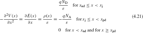
which is usually referred to as the build-in voltage with ni the intrinsic carrier concentration. Charge neutrality requires that the total charge in the n-type layer is equal to that in the p-type layer. Assuming an abrupt junction with layers of constant doping concentrations gives a positive space charge ρ(x) = qND in the n-type layer starting at x = xnd, and a negative space charge ρ(x) = −qNA in the p-type layer up to x = xpd. Using Figure 4.12 yields:
The width w = xpd − xnd depends primarily on the doping concentration of the two layers and the reverse voltage applied and follows from the Poisson equation. For a one-dimensional abrupt junction, the Poisson equation is expressed as:
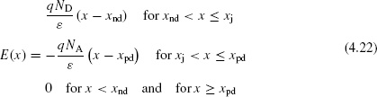
The expression for the electric field results from the space charge distribution by integration, while considering that the electric field is zero at the edges of the space charge region:
This results in an expression for the maximum electric field at the junction:
where ε denotes the dielectric permittivity. The potential distribution results from the integration of the electric field distribution, while assuming the n-well at zero-potential, as:
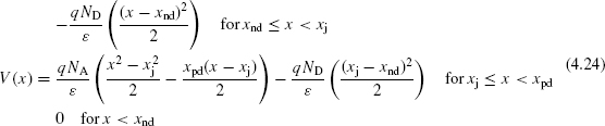
The potential at the p-type substrate can be found as:

Equating this expressing to Equation (4.19) for the build-in voltage drop (V(xpd) = Vbi), while using Equation (4.20) yields:

This equation defines the boundaries between the three different layers and the photocurrent densities are derived from the respective continuity equation. The band bending represented by Vbi can be electronically modulated using an external voltage across the pn junction, as shown in Figure 4.12. At the indicated polarity a reverse voltage is applied and the depletion layer width is increased. The maximum electric field also increases, which can be demonstrated by replacing the term Vbi in Equation (4.26) with Vbi + Vrev and inserting the result in Equation (4.23):

Since the positions of the boundaries are now known, the different photocurrent components can be derived. In the following section, the expressions for photocurrent density (i.e. the area-normalized photocurrent) are derived.
4.5.2 Electron–hole Collection in the Depletion Layer
In the depleted layer the transit time is sufficiently short to disregard carrier diffusion and recombination. The current density due to holes collected at the p-type layer contact (or electrons collected at the n-type layer contact), Jd, is directly proportional to the photon absorption within the depletion layer and yields:
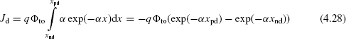
A sufficiently high reverse voltage results in a depletion layer extending up to the detector surface (xnd = xnd = 0); this expression simplifies to Equation (4.2). Depleting the p−-epilayer in a CMOS process is possible with acceptable values for Vrev. However, this is not the case for the depletion of the entire substrate. As a consequence electrons photogenerated in the bulk substrate and diffusing towards the depletion layer are a significant part of the photocurrent detected at the n-well contact.
4.5.3 Electron–hole Collection in the Substrate
When assuming the entire n-well depleted from the junction up to the surface, the minority charge carrier transport in the nondepleted p-type bulk (i.e. assume E(x) = 0 and ∂E(x)/∂x = 0) is described by the continuity relation as:
with τn the electron lifetime in the p-substrate. Solving the continuity relation while assuming boundary conditions (n(xpd) = npo = 0 and p(xpb) = npo = 0) and disregarding recombination (R(x) = 0) yields for xpd < x < xpb:
where Ln = (Dnτn)1/2 denotes the diffusion length of electrons in the p-type layer. State-of-the-art IC processing ensures that αLn ![]() 1 over the entire visible spectral range and thus Equation (4.30) simplifies to:
1 over the entire visible spectral range and thus Equation (4.30) simplifies to:
Depending on wafer size xpb > 500 μm and exp(−αxpb) ![]() exp(−αxpd). Moreover, exp(−xpb/Ln)
exp(−αxpd). Moreover, exp(−xpb/Ln) ![]() exp(−xpd/Ln). When assuming front-side illumination Equation (4.31) yields:
exp(−xpd/Ln). When assuming front-side illumination Equation (4.31) yields:
The current density Jp can be calculated from the continuity relation:
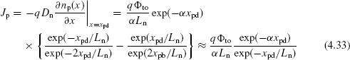
An expression is found for the photocurrent due to direct charge collection in the depletion layer in addition to the collection of photogenerated charge in the bulk that diffuses towards the depletion layer by adding Equation (4.28) for xnd = 0 and Equation (4.33) for xpd ![]() Ln, which yields:
Ln, which yields:
The efficient collection of especially long-wavelength light (i.e. with such a value for the absorption coefficient that α(λ)xpd ![]() 1) requires a high-quality material with a large minority carrier diffusion length.
1) requires a high-quality material with a large minority carrier diffusion length.
4.5.4 Electron–hole Collection Close to the Surface
The assumption of a depletion layer extending into the n-well up to the surface is rather unrealistic. The surface is an obvious discontinuity of the regular lattice of the silicon crystal and a source of recombination traps. Moreover, constant doping concentration up to the surface is difficult to achieve. The net effect is an electric field in a narrow region directly adjacent to the surface in which minority charge carriers are driven towards the surface where recombination takes place. These effects can be included in the responsivity calculations by assuming a small depletion layer at the surface with high surface recombination velocity, which effectively drains away the part of the incoming photon flux absorbed therein. In Figure 4.12 the boundary of this depletion layer is included as xns. Any nondepleted part of the n-well is sandwiched in between two depletion layers and photogenerated charge ends up in any of these depletion layers by diffusion. Calculation of this component, Js, is similar to the calculation of the photogenerated charge in the bulk and uses the continuity relation for holes in the n-well:

with τp the hole lifetime in the n-well. The solution of this continuity relation when assuming simplified boundary conditions (p(xns) = pno and p(xnd) = pno) and disregarding recombination (R(x) = 0) is:

with Lp = (Dpτp)1/2 as the diffusion length of holes in the n-well. The terms exp(−xns/Lp) and exp(−xnd/Lp) are small, but, unlike the case of the bulk-generated minority charge carriers, in the same order of magnitude. Therefore, none of these can be disregarded and Equation (4.36) simplifies to:


Figure 4.13 Responsivity of an actual n-well-p-substrate photodiode. The quantum efficiency is reduced at wavelengths shorter than 400 nm due to surface absorption, and at wavelengths beyond 700 nm due to finite value of the minority carrier diffusion length in the p-substrate
The density of the photocurrent that is generated in the nondepleted n-well and drained into the surface depletion layer, Js results in:
This expression indicates that photon collection in the n-well is basically a topological problem. If the depletion layer does not extend far from the junction into the n-well, a large fraction is lost. This is prevented when the n-well is depleted as far as possible up to the surface.
The photocurrent density flowing into the n-well contact is found by combining Equations (4.34) and (4.38), which yields:
The remaining challenge is finding realistic values for the term xns. These can be derived by changing the boundary conditions for solving the continuity expression, Equation (4.35) from p(xns) = pno to p(xns) = (Dp/St)(dp/dt)|xns) and by using the appropriate data on surface recombination velocity, St. Practical values are in the range of xns = 0.02 μm to 0.05 μm. A typical responsivity curve is shown in Figure 4.13.
4.5.5 Backside-illuminated Pin Photodiode
The significantly reduced responsivity for wavelengths beyond 700 nm due to the finite diffusion coefficient in the substrate is clearly shown in Figure 4.13(b). However, the degrading performance at wavelengths below 400 nm is less evident. This is partly due to the pessimistic assumptions made with respect to the doping profile of the n-well. In a practical device the doping concentration increases towards the surface. The effect on collection efficiency directly follows from the current density equation for the neutral part of the n-well. When assuming flat-band conditions (no bending of the energy band diagram at the surface due to the surface potential – see Section 4.7.3) and low surface recombination velocity, the electron current density towards the surface must be zero (excess charge carriers have nowhere to go). Hence:

Figure 4.14 Backside-illuminated pin photodiode for improved response in the UV and near-IR
A positive doping gradient towards the surface results in a field which repels electrons from the surface. Although this electric field is relatively weak, it is sufficient to ensure efficient collection in the n-well–p-epilayer junction up to the surface depletion layer boundary at xns [22]. The complication results from ensuring flat band. Using the polysilicon gate is counter-productive due to the optical absorption within this gate. Special processing on the oxide is more effective, but is poorly compatible with CMOS processing. The solution is to separate the CMOS process from the surface processing required for optical purposes by using backside illumination, as shown in Figure 4.14.
The backside processing can, in principle, be optimized to suit optical requirements. The coating thickness can be designed for a particular transmission and the backside p-type doping profile for a well-defined doping gradient. Furthermore, ion implantation can be used with a dose sufficient to ensure flat band. The disadvantage is the long diffusion of excess charge carriers towards the n-well–substrate junction. This problem is solved when using a very low doped substrate. In that case the entire substrate can be depleted using moderate levels of the reverse voltage. When the substrate doping concentration, NA, is in the same order of magnitude as the intrinsic doping concentration, ni, the substrate is intrinsically doped and is generally referred to as a pin diode. Depleting the substrate down to the backside basically eliminates the wafer diffusion photocurrent and thus also improves long-wavelength response.
High-resistivity wafers are not directly compatible with CMOS processing; thus other approaches are being used. Since the electrical interconnect of the backside-illuminated diode is now on the backside of the system, the CMOS wafer is often bonded onto another support. This could be another silicon wafer with an interconnection pattern. The advantage is the protection of the CMOS devices. Moreover, Micro-ElectroMechanical System (MEMS) technologies are subsequently used for thinning the CMOS wafer to 10 μm to 50 μm in thickness to enable efficient charge collection with moderate values of the reverse voltage, while using standard CMOS substrates. Through-wafer micromachining for backside contact is also used to improve system integration. The resulting system features a nearly perfect spectral response over the entire visible spectrum and is used for metrological purposes [23].
4.5.6 Electron–hole Collection in Two Stacked pn Junctions
The photodiode structure shown in Figure 4.12 is not the only possible device in a CMOS process. When including the drain/source implantation, two stacked junctions result and, consequently, two stacked photodiodes, as shown in Figure 4.15.
The expressions for the photocurrents in the upper and lower junction are not fundamentally different form those already derived in the previous section on the single junction photodiode. Hence, the results can be applied with the obvious adaptations in variables. The double-junction detector is basically a three-terminal device with the n-well draining the photogenerated electrons collected at the upper and lower junction. The shallow p-type (SP) layer contact is used to read the photocurrent of the upper junction only and the substrate that of the lower junction. The loss in photogenerated charge due to recombination in the bulk substrate is accounted for in the response of the lower-junction photodiode, whereas the surface recombination adversely affects the detectivity of the upper photodiode.
The essential difference between the single pn junction and the stacked photodiodes is that the stacked junctions compete for the collection of the photogenerated charge in between the junctions. Basically, the upper diode is efficient in collecting shallowly generated charge, whereas the lower junction efficiently detects the bulk-generated charge. Short-wavelength visible light is shallowly absorbed, because of the high value for the absorption coefficient, whereas the longer-wavelength light penetrates more deeply into the material. As a consequence the upper junction reveals a relatively high responsivity for blue light, whereas the lower more efficiently detects red light.

Figure 4.15 Schematic cross-sectional view of a reverse-biased pn junction used for photon detection. Three photocurrent components can be identified due to the presence of a depletion layer of width Wdepl

Figure 4.16 Responsivity of the SP-n-well junction (upper) and the n-well-p-substrate junction (lower) with Vrev =1V applied across each junction
Figure 4.16 shows the typical response curves for photodiodes fabricated in a CMOS process. The wavelength-dependent response in stacked photodiodes can be used for color sensing, which is demonstrated in the application example in Section 4.8.1.
Comparing Equations (4.28) and (4.34) reveals that both depleted and nondepleted absorption volumes result in efficient and well-defined photogenerated charge collection, provided that the minority carrier lifetime is sufficiently long. The essential advantage of charge collection in a depleted layer is in the dynamic performance. Charge collection is governed by the drift velocity of minority carriers in the electric field, as defined by Poisson's equation and a reverse voltage can be selected to yield a transit time that is orders of magnitude smaller than charge collection by diffusion. The reverse-biased pn junction has a strongly reduced junction capacitance, which also contributes to the fast response. The maximum reverse voltage level is, in principle, limited by breakdown; however, a specially designed avalanche-type photodiode (discussed in Section 4.7.2) can be operated at breakdown to achieve charge-carrier multiplication and hence provide opto-electrical gain.
The drawback of a reverse-voltage operated photodiode is the increased leakage current. The leakage current directly determines the shot-noise level of the diode and limits detectivity. The detection limit of the optical system is determined by the combined effect of the detector and the readout circuits. A major design issue is, therefore, where to implement gain in the opto-electrical system; in the photon detector or the readout circuit. Providing guidelines for addressing this question requires the analysis of the noise behavior of the photodiode, while including that of the readout circuit.
4.6 Detection Limit
The key performance specification of a sensor is the detection limit. In an optical sensor the detection limit is the minimum light intensity that can be reproducibly measured. The detectivity D* is used for specifying detection limit. This parameter is the inverse of the detection limit and is normalized on detector area and bandwidth. The detection limit is affected by the following three factors:
(1) Environmental, such as stray light and temperature;
(2) Detector characteristics;
(3) Readout.
These are discussed in this section.
4.6.1 Noise in the Optical Signal
The optical measurement includes two major fundamental sources of uncertainty. The first is the influence of optical power due to unwanted background radiation. The second is the random variations in the stream of photons entering the detector. Both contribute to the detection limit in the photon detector.
Typically, a photon detector is used to measure the optical power of a source or a scene in the presence of a background at a certain temperature. This temperature could be room temperature, which in that case is an important issue in infrared detectors, but less so for silicon-based photon detectors operating in the visible spectral range. However, this could also be the diffused reflection of an illuminating source by the background. In that case the lamp temperature has to be considered. The background optical power directly follows from Planck's radiation law as:
In this calculation the entire optical system must be included. A simplified system is considered here with a lamp of peak emission within the silicon spectral range (central frequency, υ ≈ 6 × 10¹⁴ Hz), which remains constant over the silicon bandwidth (Δυ ≈ 8 × 10¹⁴ Hz). Moreover, A denotes the aperture area of the lens, Ω the field of view (Ω ≈ φ2, with φ the opening angle). Assuming AΩ ≈ 10−9 m2 and Tlamp = 1500 K yields: Popt = 50 mW. The optical system must be able to distinguish between the reflected background power and the power of the intended radiation.
As is mentioned in Section 4.2, incident radiation of optical power Popt and wavelength λ produces electron–hole pairs at an average rate given by: Φeh = Popt/hPυ in an ideal photon detector. In the quantum-mechanical description of radiation, the optical power is due to the cumulative energy of a stream of photons (Popt = Φph × Eph) = Φph × (hPυ). However, this incident stream of photons is due to a random process and obeys Poisson statistics. The absorption of photons is also a random process. Some photons penetrate more deeply than others of the same wavelength. The decrease in photon flux described in Equation (4.1) is an averaging of the radiation–crystal interactions. Finally, the collection of the photon-generated electron–hole pairs is also a random process. As described in the previous section, some minority charge carriers need to diffuse over a substantial length of detector material before being collected at the junction. The combined effect of these random processes is described by the shot noise expression for photocurrent:
where B denotes the bandwidth of the optical signal. Usually, the noise spectral power sn = in2/B [A2/Hz] is used.
Since the shot noise spectral power is proportional to the photodiode current, it is important to determine the minimum current in the photodiode in the absence of light. This property is generally referred to as the dark current or leakage current and depends on material properties and diode biasing.
4.6.2 Photon Detector Noise
The equivalent noise sources of the photoconductor and photodiode are derived in this section and also compared to the typical equivalent input noise level of readout circuits.
The photoconductor is basically a resistor of nominal (nonilluminated) resistance Ro = 1/σo with the noise performance determined by the well-known expressions for thermal noise:
where B denotes the bandwidth of the optical signal. The two parts of this expression are equivalent. The first defines the equivalent noise voltage and the second the equivalent noise current of the resistance. The conventional technique for photoconductance readout involves an excitation voltage and the measuring of the resulting current (Figure 4.9). Hence, the current-to-voltage converter (trans-resistance circuit) is used for readout.
The leakage current in a pn junction without illumination is essential for estimating the shot noise level and can be found from the continuity expression (Equation (4.29)) with G(x) = 0 as:
where Jso denotes the reverse saturation current density of the diode. Typical values are in the range 10 nA/m2 < Jso < 10 μA/m2. However, it should be noted that for a very small junction area or for long, high-aspect ratio junctions, Iso is primarily determined by the perimeter length. Equation (4.44) reveals a fundamental dilemma in photodiode readout design. When short-circuiting the junction (Vrev = 0, which is generally referred to as the photovoltaic mode of operation), the dark current is limited to the saturation current: Idark = −Iso, whereas the dark current increases exponentially with reverse voltage. Hence, the benefits of an increased depletion layer width in terms of improved responsivity by applying a reverse voltage (Vrev > 0 V in Figure 4.11, the photocurrent mode of operation), as discussed in Section 4.5, are at the expense of an increased dark current and consequently at the expense of an increased shot noise level. In an AD = 100 × 100 μm2 photodiode, the dark current is typically equal to: Idark = JdarkAD = 10−28exp(qVrev/kBT). The noise current at Vrev = 1 V is typically equal to:
The detection limit follows when the SNR and noise bandwidth specification, B, are included. In the case of SNR = 10 dB and B = 100 Hz, the detection limit is at: ![]() SNR = 16 × 10−26 A2, thus iph,det = 0.4 pA.
SNR = 16 × 10−26 A2, thus iph,det = 0.4 pA.
In optics the measurand is optical power. Therefore, it is customary to specify noise level in terms of Noise Equivalent optical Power (NEP), which is equal to total noise power divided by the opto-electrical conversion, the responsivity, R:
Moreover, the reciprocal specification is used for the detection limit in terms of optical power and also includes detector area AD (traditionally in [cm2]) and bandwidth to facilitate the performance comparison of detectors of different sensitive area. This figure-of-merit of the detector is usually indicated as D* with:
Whether the exponential increase in leakage current with reverse voltage is actually a performance limitation depends largely on the noise generated in the readout circuits. Photovoltaic readout involves direct voltage measurement for which a voltage amplifier is conventionally used. The current-to-voltage converter presented in the next section is typically used for the photocurrent readout of a reverse-biased photodiode.
4.6.3 Photon Detector Readout
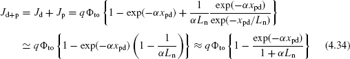
The equivalent circuit diagram of a photovoltaic operated photodiode is shown in Figure 4.17. It is composed of a series bulk resistance, which gives rise to thermal noise as represented by noise voltage un, with noise spectral power suns = 4kBTRs, and a parallel impedance, Zp, which is composed of the small-signal dynamic resistance, rd, parallel to a very large leakage resistor, Rp > 10 MΩ, and the diffusion capacitance Cd: Zp = rd/(1 + jωrdCd), with rd = ∂Ud/∂Id = ∂[(kBT/q) × ln(Id/Is)]/∂Id = kBT/(qId), with Is the Id-independent saturation current. The thermal noise in the bulk resistance dominates noise performance, where un is in the range of (1 to 100) pV/Hz1/2, typically.
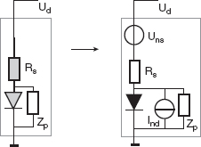
Figure 4.17 Sources of noise in a photovoltaic operated photodiode
Figure 4.18 Sources of noise in a reverse-biased photodiode
The equivalent circuit diagram of the reverse-biased diode is shown in Figure 4.18. Although the same components are included in the circuit, their values are significantly different. The differential resistor rd is in the reverse-biased diode set by the negative value of the voltage applied: 1/rd = ∂Id/∂Ud = ∂[Isexp(qU−/kBT)]/∂Ud = ∂(Is × 0)/∂Ud = 0, since U−/(kBT/q) → −∞. Hence, rd → ∞. The charge storage in a reverse-biased junction is determined by the space charge layer boundaries of the depleted region and specified by Cb and Zp = Rp/(1 + jωRpCb). Since Rp ![]() Rs, uns is insignificant and the noise is set by the diode shot-noise, ind. Considering the very low leakage currents in state-of-the-art diodes at moderate values of the reverse voltage, in,eq = (2qId)1/2, which yields (10 to 100) fA/Hz1/2, typically. It should be noted that Zp is capacitive throughout most of the practical frequency range.
Rs, uns is insignificant and the noise is set by the diode shot-noise, ind. Considering the very low leakage currents in state-of-the-art diodes at moderate values of the reverse voltage, in,eq = (2qId)1/2, which yields (10 to 100) fA/Hz1/2, typically. It should be noted that Zp is capacitive throughout most of the practical frequency range.
The operational amplifier (opamp)-based implementation of the trans-resistance circuit including the opamp equivalent input noise sources is shown in Figure 4.19. The signal source is assumed to be ideal. The equivalent input noise sources of the opamp are specified as: un1 and in1.
The noise power at the output is expressed as:
The equivalent input current source follows as:

Figure 4.19 Trans-resistance amplifier for photodiode readout
Assume the following highly competitive noise specifications for the operational amplifier: equivalent input noise voltage spectral power sun = 10−17 V2/Hz and equivalent noise current spectral power sin = 10−26 A2/Hz. The circuit is designed for a trans-impedance Uo/Ii = 105 V/A using Rf = 100 kΩ, which results in an equivalent input spectral noise power (4kBT = 1.65 × 10⁻²⁰ J) equal to:
The noise due to the feedback resistance dominates noise performance. Increasing the feedback resistance up to Rf = 1 MΩ provides both conversion gain and reduces the equivalent input noise current to: sin = 2.75 × 10⁻²⁶ A2/Hz. The problem of this solution is twofold. Firstly, due to the junction capacitance of the reverse-biased diode, peaking in the spectral response of the readout occurs [24]. This effect can be avoided when using a small capacitor parallel to the feedback resistance. Secondly, the photodiode noise remains orders of magnitude lower (compare Equation (4.50) with Equation (4.45)) and is ultimately limited by the equivalent input noise current of the opamp. The detrimental effect of the exponential increase of the dark current with reverse voltage is, therefore, often of limited practical importance. Nevertheless, high-performance photon detection would benefit from a reduced dependence on the equivalent input noise level of the readout circuits.
The noise performance is somewhat different in the case of photovoltaic readout. The (1 to 100) pV/Hz1/2 of the photodiode is in series with the opamp equivalent input noise voltage of 3 nV/Hz1/2. The feedback components provide additional noise. Consequently, also in the case of photovoltaic readout, the noise performance is spoilt by the readout. A similar conclusion can be derived for photoconductor readout. The fact that readout dominates noise performance calls for the implementation of gain in the photon detector itself, which is discussed in the next section.
4.7 Photon Detectors with Gain
In principle, there are three approaches available for providing gain in the photon detector itself:
(1) Phototransistor
(2) Avalanche photodiode
(3) Time integration of photon-generated charge
The merits and limitations of these techniques are discussed in this section.
4.7.1 The Phototransistor
The bipolar transistor is well known for providing current gain. Hence, using the photodiode as a base–emitter or a base–collector junction and adding the third terminal would, in principle, create interesting options for the realization of a photon detector with internal gain. The CMOS process does provide a (parasitic) vertical pnp transistor when using the SP (drain/source) within an n-well as emitter, the n-well as base and the p-epilayer as (common) collector. Lateral npn and pnp transistors are also feasible. If these transistors are of insufficient performance, one could consider using a BiCMOS or a dedicated bipolar process for on-chip integration of the opto-electronic system.
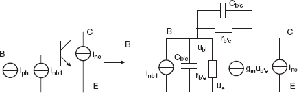
Figure 4.20 Phototransistor including noise sources
Figure 4.20 indicates that current gain equal to the common–emitter current gain βF is indeed provided by leaving the base terminal open, while measuring the collector current. Unfortunately, the noise current is amplified by the same factor and thus the collector shot noise should also be considered. Moreover, the dynamic performance of the npn phototransistor is seriously reduced as compared to the basic pn junction, due to capacitive loading within the device. For these reasons the phototransistor is not frequently used.
4.7.2 The Avalanche Photodiode
The avalanche photodiode is similar to the conventional pn junction, apart from the fact that the doping levels are relatively high. The operation of the avalanche photodiode is based on impact ionization within the depletion layer. The basic device structure is shown in Figure 4.21.

Figure 4.21 The avalanche photodiode
The doping concentration of the p++ layer exceeds 1019 cm−3 and n+ is in the order of 2 × 1018 cm−3 (this is generally referred to as the single-sided abrupt junction). Under these conditions and Vrev ![]() 10 V, Equation (4.27) reduces to:
10 V, Equation (4.27) reduces to:

At such extremely high values for the electric field, electron–hole pairs in the depletion layer gain sufficient energy to cause impact ionization. The probability of an electron generating an extra electron–hole pair is characterized by the electron ionization coefficient α, whereas the hole ionization coefficient is defined as β. Since the total photocurrent should remain constant throughout the depletion layer the following set of equations result:

where M denotes the avalanche multiplication factor and Ipn represents the collected photocurrent in a low-field pn junction without avalanche gain. The electron current in the p++ layer leaving the depletion layer (i.e. electrons entering the depletion layer) In(0) = Ipn, whereas the hole concentration Ip(0) = M × Ipn,. Similarly in the n+ layer In(wdepl) = Ipn, and Ip(wdepl) = M × Ipn. The coefficients α and β are generally unequal and strongly depend on the electric field and, thus, on the position x in the depletion layer. Nevertheless, when assuming α = β an adequate expression for avalanche multiplication is obtained:
Hence:
Considering that In(0) = Ipn and In(wdepl) = M × Ipn, the expression for avalanche multiplication results as:
The avalanche multiplication (Equation (4.55)) becomes infinite if the integral becomes unity, which represents avalanche breakdown. For high sensitivity the device should be operated as close as possible to avalanche breakdown in order to maximize gain.
Maximizing gain does not necessarily imply the best detection limit. The noise in the avalanche photodiode depends on both the shot noise in the photocurrent and the variations in the multiplication factor M due to random variations in the actual positions where impact ionization in the space charge region takes place. The shot noise power is, therefore, multiplied with the power gain M2 and the impact ionization position uncertainty is incorporated in the expression for the equivalent spectral noise using the excess noise factor, F(M):
Practical values of F(M) are in the range M0.3 < F < M1. As a consequence the noise spectral power increases with avalanche gain by more than a factor of M2, whereas the signal gain is proportional to M2. Since the signal-to-noise ratio within the photodiode decreases with avalanche gain, it seems legitimate to wonder what the benefits are. The answer is given in the comparison between Equations (4.56) and (4.45). As is concluded in the previous section, the noise in photodiode readout is dominated by the circuit. Therefore, increasing the photodiode signal level does improve detectivity despite the fact that the photodiode equivalent spectral noise current increases by a factor that is higher than the signal gain.
This can be demonstrated by referring again to the current-to-voltage converter in Figure 4.19 with the feedback resistance Rf = 1 MΩ, which is characterized by an equivalent input-referred spectral noise current sin = 2.75 × 10⁻²⁶ A2/Hz. The photodiode spectral noise current due to dark current is equal to sid = 1.6 × 10⁻³⁰ A2/Hz. Hence a signal of 1 Hz bandwidth and an amplitude of 40 fA (Ps = 1.6 × 10⁻²⁸ A2) is well below noise level (Pn,d + Pn,c = (1.6 × 10⁻³⁰ + 2.75 × 10⁻²⁶) A2 ≈ 2.75 × 10⁻²⁶ A2) when using a conventional photodiode. Using an avalanche photodiode with reverse voltage close enough to avalanche breakdown to give M = 50 results in a signal power M2 × Ps = 4 × 10⁻²⁴ A2 and a noise power M3 × Pn,d = 2 × 10⁻²⁵ A2 ![]() Pn,c (worst case, F(M) = M, is assumed). The avalanche gain has lifted the signal above the noise level of the readout and the overall noise performance is limited by the photodiode. Obviously, an optimum results if the gain is set to such a value that the photodiode spectral noise is equal to the input-referred spectral noise of the readout:
Pn,c (worst case, F(M) = M, is assumed). The avalanche gain has lifted the signal above the noise level of the readout and the overall noise performance is limited by the photodiode. Obviously, an optimum results if the gain is set to such a value that the photodiode spectral noise is equal to the input-referred spectral noise of the readout: ![]() × Pn,d = Pn,c = 2.75 × 10⁻²⁶ A2. Hence, Mopt = 25.8 with SNR =
× Pn,d = Pn,c = 2.75 × 10⁻²⁶ A2. Hence, Mopt = 25.8 with SNR = ![]() dB in this particular opto-electronic system.
dB in this particular opto-electronic system.
The maximum avalanche multiplication is limited in a practical diode to M ≈ 100 due to lateral fluctuations in doping concentration. Since the avalanche breakdown voltage depends on doping concentration, the reverse voltage applied must be below the breakdown voltage minus some margin to avoid localized breakdown. This in turn limits the achievable gain. The avalanche multiplication takes place close to the junction in the bulk. The very high doping concentrations in the p and n layers result in a relatively short minority carrier lifetime. As a consequence the avalanche photodiode has a relatively strong spectral dependence with a peak response in the (500 to 600) nm range. Special structures have been reported with a shallow junction and a selective UV/blue response [25]. Applications are mainly in medical imaging based on scintillating materials on top of a detector array.
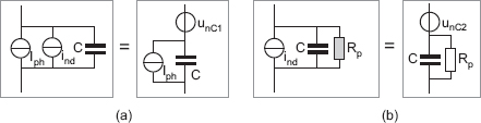
Figure 4.22 Using a capacitor for integration of photon-generated charge
4.7.3 Time Integration of Photon-generated Charge
Time integration can be used for enhancing SNR in low-bandwidth signal readout. When considering the photodiode with dc photocurrent and equivalent noise source ind with ideal capacitor C, as shown in Figure 4.21. The integrated charge due to the dc signal after time ti is equal to: Q = Iph × ti and results in a voltage VC = Q/C = Iph × ti/C. The equivalent noise voltage can be approximated using Figure 4.22(a) as:

This expression suggests an unlimited improvement of SNR with integration time. However, an ideal capacitor is assumed. A practical integrator is modeled as a lossy capacitor, as shown in Figure 4.22(b), and its noise behavior is expressed as:

The noise voltage squared is determined by the combined effect. For Iph = 1 nA, C = 100 fF, ti = 20 ms and 4kBT = 1.65 × 10⁻²⁰ J the result is:

Hence the kBT/C noise can usually be disregarded. In that case the signal power is proportional to ti2, the noise power is proportional to ti, and SNR = Ps/Pn = (2π2Iph/q)ti. An array of photodiodes with charge integration in the junction capacitance of the reverse-biased junction is the basis of the well-known CCD imager. The alternative is an array of MOS-based capacitive photon detectors
Figure 4.23(a) shows the NMOS transistor without a drain or a source and operating as capacitive detector. When assuming equal work function for the polysilicon gate and the p-type silicon epilayer, the energy bands are flat in the case of gate–substrate voltage VGS = 0 V (dashed lines in Figure 4.23(b)). Applying a negative potential to the gate with respect to the silicon results in depletion of the silicon from the surface and bending of the energy bands as shown by the solid lines in the figure. The work function of polysilicon (qϕSi) is assumed to be equal to that of silicon. A further increase in the amplitude of the negative potential beyond the threshold voltage results in inversion. In this state any available free electrons are attracted and the part of the p-epilayer directly below the surface effectively turns into n-type. Consequently, the device provides depleted volume under the gate area that is suitable for storage of photon-generated minority charge carriers in the p-epilayer/substrate. Any stored charge is immediately released when switched to a positive gate potential and can be measured as a current pulse. Operating the NMOS photon detector, therefore, involves applying a negative gate potential during charge integration and release of the charge by applying a positive pulse to the gate (for reset or charge transfer). The PMOS transistor can be used for charging photon-generated carriers in a similar way.
Figure 4.23 NMOS photon detector: (a) structure and (b) energy band diagram
4.8 Application Examples
4.8.1 Color Sensor in CMOS
The two vertically stacked pn junctions that come with a CMOS process can be used for the simultaneous measurement of light intensity and color without using an optical filter. The shallower junction is between the drain/source p-type layer and the n-well, whereas the deeper junction is between the n-well and the p-epilayer [26]. The different spectral response curves of these photodiodes are shown in Figure 4.16 and are discussed in Section 4.5.5. The absorption volume in between the p+–n-well junction and the n-well–p−-epilayer junction is shared between the two junctions. The reverse voltage between the two respective junctions can be controlled in such a way that the depletion layers meet and the entire n-well is depleted. The upper absorption volume contributes to the shallow junction photocurrent and the lower absorption volume contributes to that of the lower diode. As impinging blue/UV light is already fully absorbed within a depth less than 0.5 μm, such short wavelength light contributes to the photocurrent of the upper junction only. Similarly, longer wavelength light predominantly generates photocharge at larger depths and thus contributes mainly to the lower-junction photocurrent.
The depth of the actual boundary between the space charge layers can be electronically programmed, by changing the reverse voltages applied across the junctions. Increasing the reverse voltage applied across the upper junction and simultaneously lowering the voltage across the deeper junction increases the longer wavelength response of the upper junction at the expense of that of the lower junction. The n-well contact supplies both the p+-layer–n-well photocurrent, Iu, plus the n-well–p-epilayer photocurrent, Il, and thus is a good measure for the responsivity to total incident photon flux, Ru + l. The photocurrent measured at this terminal is, therefore, the intensity signal. The responsivity of the upper junction (the drain/source contact), Ru, divided by the responsivity at the n-well contact, Ru + l, is a good measure for the spectral information and is referred to as the color signal: Ru/Ru + l. Figure 4.24 shows these spectral response curves.

Figure 4.24 Responses of the color sensor: (a) adding the photocurrent provided by upper and lower junction using the n-well current to give the intensity signal and (b) normalizing the upper junction photocurrent to the intensity signal to provide the color signal
Several circuits are suitable for the readout of Iu/(Iu + Il) or Il/(Iu + Il). A very convenient realization is based on the voltage switching AD converter, which provides a digital output code directly proportional to the color signal. The schematic block diagram and timing diagram are shown in Figure 4.25. The reverse-biased junction capacitors are used as storage elements. Two conversion cycles are needed to measure both signals. In the first phase, Iu plus Il are integrated and during the second phase only the current provided by the lower junction is integrated. Four states can be distinguished. During the first two states, S2 is closed. During state(1), S1 closes and both junctions are charged to VDD = 5 V. Subsequently, S1 is opened and during state(2) the junctions are discharged by Iu + Il until the lower threshold voltage of the comparator is reached. During state(3) and state(4), S2 remains open and the junctions discharge using Il only. Two 16-bit counters are used to store the data from which the intensity and color signal can be calculated. This technique does not allow an accurate definition of the space charge regions of the upper and lower photodiode, but the color signal is sufficiently pronounced so that it can be used for object identification based on color.
Figure 4.26 shows the photograph of the optical system, which is used to identify illumination with different light sources. The sensor performance enables the identification of indoor or outdoor operation, which can be used by an operator to adapt the brightness of a display of a tool or instrument.

Figure 4.25 Readout circuit of the color sensor
4.8.2 Optical Microspectrometer in CMOS
An integrated optical microspectrometer can be fabricated in CMOS using the Fabry–Perot interferometer, which is in principle composed of two highly-reflective parallel mirrors spaced a well-determined distance apart with the reflecting part facing each other. The space in between the mirror surfaces is essentially a resonance cavity. An optical microsystem has been fabricated and is composed of 16 Fabry–Perot resonators of different fixed cavity spacing on top of 16 integrated photodiodes. After fabrication of the circuits for channel selection and readout, the lower thin-film metal layer is deposited and patterned. Subsequently, oxide layers are deposited to space the mirrors, thus ensuring parallel mirrors. Four subsequent masked oxide etch steps are applied to fabricate cavities of 16 different thickness. The 16 channels are designed to cover the entire visible spectral range. The fabrication of each of these Fabry–Perot resonators shown in Figure 4.27, is compatible with a standard CMOS process, thus enabling, the on-chip integration of circuits for selection and readout of the array photodiodes covered by the different resonators.

Figure 4.26 Microphotograph of the color sensor
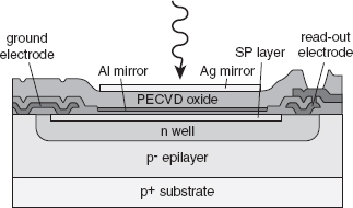
Figure 4.27 CMOS post-processing for fabrication of a Fabry-Perot element
The resulting device is shown in Figure 4.28 [27]. An additional channel is used for the compensation of dark current and the scattering, which is due to the roughness of the mirrors. The PECVD oxide is deposited on top of the lower mirror surface. For this reason silver cannot be used for the lower mirror and a silicon(CMOS)–aluminum-oxide–silver stack is used instead.
A critical factor in the fabrication of this microspectrometer is the etching of the PECVD silicon oxide into 16 different thicknesses using four masks. Basically a first mask is used to etch 50 % of the oxide over 50 % of the elements. Subsequently a second mask is applied and an additional 25 % of oxide is removed over 50 % of the elements already attacked in the first etch in addition to 50 % of the elements with oxide coating which have not yet been thinned. A third and fourth mask are applied to remove another 12.5 % and 6.25 % of the oxide thickness. A careful mask design results in 16 elements, each with a different thickness of the oxide coating. The complication is the timed etching of oxide, which requires accurate characterization of the etch rate. Figure 4.29 shows the result of the first-generation of these devices, which were designed to cover the entire visible spectrum. However, these were over-etched.

Figure 4.28 16-channel CMOS microspectrometer using integrated Fabry–Perot elements

Figure 4.29 Spectral response curves of the 16-channel CMOS micro spectrometer
4.9 Summary and Future Trends
4.9.1 Summary
In this chapter the merits and performance limitations of CMOS-compatible photon detectors in the 300 nm to 1000 nm spectral range are discussed. Firstly, the general issues that determine the spectral response are discussed. These are:
(1) The wavelength dependence due to the thin-film coating of the silicon absorber;
(2) The wavelength dependence of the silicon absorption coefficient;
(3) The wavelength dependence introduced by the collection of photogenerated excess charge carriers.
Subsequently, two types of detectors have been considered:
(1) Photoconductors;
(2) Pn junction-based photon detectors.
Although photoconductors can provide gain, these feature a less favorable detection limit and high gain is associated with poor dynamic performance. Therefore, the emphasis is put on pn junction-based photon detectors. The simplest realization is the photodiode. Two charge collection regimes are identified: drift in depletion layer and diffusion in nondepleted parts of the silicon. The latter introduces performance limitations, which are overcome in pin-type of photodiodes and backside-illuminated photodiodes.
A major limitation of the basic photodiode is that it does not provide gain, which results in a detection limit generally set by the readout circuit. Hence, pn junction based devices are discussed that are intrinsically suitable for providing gain. These are:
(1) The phototransistor;
(2) The avalanche photodiode;
(3) The combination of photodiode with capacitor for charge integration.
The avalanche-operated photodiode is especially suitable for matching the photodiode noise performance to that of the readout circuit. The viability of CMOS-based opto-electronic systems is demonstrated using two realized designs:
(1) A color sensor;
(2) A microspectrometer.
4.9.2 Future Trends
The most-demanding challenges of device research in the field of silicon photon detectors are in the ultraviolet (UV) spectral range. The absorption coefficient limits penetration to 10 nm and surface effects dominate performance.
MEMS technologies are increasingly being used to improve detector performance, to facilitate system integration or to enable implementation of optical detectors in an application.
The spectral response in the visible spectral range can be almost perfect when applying the techniques discussed in Section 4.6. As a result, silicon photon detectors are increasingly investigated in combination with scintillating materials for operation in spectral range where silicon is not very suitable, such as X-ray. Many applications are in the medical field.
Fabrication of photon detector and readout circuits in an IC-compatible process (preferably CMOS) does not generally provide the best possible detector response in a particular application. The vertical doping profiles are selected for operation of the active devices and do not necessarily provide high opto-electrical efficiency. As is shown, the spectral performance is particularly sensitive to details in the vertical doping profile in the UV/blue and near-IR spectral range. Other ‘costs’ are the need for an additional metal layer to provide shielding of the circuits for light, which would otherwise cause increased leakage current, and the enlarged die area. Therefore, the CMOS opto-electronic system is likely to find application only if the benefits do actually pay off. This has already been demonstrated for array-type systems, such as the CMOS camera, but may also prove decisive in high-resolution microspectrometers.
The second group of opto-electronic systems that is likely to benefit from the on-chip co-integration in a CMOS process comprises those that require either a huge amount of (analog) signal pre-processing, or are vulnerable to parasitics.
The third group of promising CMOS opto-electronic systems are application-driven and require a single photon detector of modest performance to serve a potentially high-volume application, such as a simple color sensor. Such a system would have to compete with the more-established approaches, which involve the deposition and patterning of color dyes in post-IC processing steps. Such post-processing steps pay off in array detectors (CMOS cameras), but not necessarily if only one detector is required.
Although the indirect band gap in silicon does not allow efficient light emission, the material is very suitable for the fabrication of integrated optics systems [28].
Problems
4.1 Relation between quantum efficiency and responsivity
The external quantum efficiency of a silicon photon detector is specified as η = 0.8 for λ = 500 nm. Calculate the equivalent responsivity, R, when Planck's constant is given as hP = 6.6 × 10⁻³⁴ J/s and the unit charge q = 16 × 10−20 C.
4.2 Gain in a photoconductor
Dimension an n-type silicon photoconductor for maximum sensitivity, Δσ/qΦto Also calculate the photoconductive gain, G*, and the cut-off frequency of the detector at these dimensions when the following properties and design constraints are given:
- μn = 0.15 m2 V-1 s-1;
- τn = 2.5 × 10⁻³ s;
- Detector area AD = 1000 × 1000 μm2;
- Minimum feature size (space between lines or line width) = 10 μm;
- Vexc = 10mV.
4.3 Expressing detection limit in terms of NEP and D*
Calculate the detection limit in an opto-electronic system in terms of the noise equivalent power (NEP) and detectivity D* composed of a photodiode and current-to-voltage converter for readout. Also calculate the SNR in the case of illumination with a plane-wave front of monochromatic light source of 1 mW/m2 of optical intensity.
The following specifications are provided:
- Detector noise spectral power:
 = 1.6 × 10⁻³⁰ A2/Hz;
 - Input-referred equivalent noise spectral power of the readout: = 10.25 A2/Hz;
- Detector responsivity R = 0.3A/W;
- Trans-resistance Rf = 1 MΩ
- Noise bandwidth B = 100 Hz;
- Detector area AD = 10-2 cm2.
References
[1] Wolffenbuttel, R.F. (ed.) (1996). Silicon Sensors and Circuits: On-chip Compatibility, Chapman & Hall, London.
[2] Simpson, M.L., Nance Ericson, M., Jellison, G.E., Dress, W.D., Wintenberg, A.L. and Bobrek, M. (1999). Application specific spectral response with CMOS compatible photodiodes, IEEE Transactions on Electron Devices, 46, 905–913.
[3] Kruse, P.W. (1977). The photon detection process. In Topics in Applied Physics, Optical and Infrared Detectors, ed. R.J. Keyes, Springer, Berlin, Vol. 19.
[4] Bube, R.L. (1992). Photoelectric Properties of Semiconductors, Cambridge University Press, New York.
[5] Kingston, R.H. (1978). Detection of Optical and Infrared Radiation, Springer Series in Optical Sciences, Springer, Berlin, Vol. 10.
[6] Philipp, H.R. and Taft, E.A. (1960). Optical constants of silicon in the region 1 to 10 eV, Physical Review, 120, 37–38.
[7] Philipp, H.R. and Ehrenreich, H. (1963). Optical properties of semiconductors, Physical Review, 129, 1550–1560.
[8] Barta, E. (1977). Optical constants of various heavily doped p and n-type silicon crystals obtained by Kramers-Kronig analysis, Infrared Physics, 17, 319–329.
[9] Tacke, M. (1992). Principles of photo-electric conversion. In Sensors a Comprehensive Survey, Vol. 6, ed. Gópel, W., Hesse, J. and Zemel, J.N., VCH, pp. 78–95.
[10] Singh, J. (1995). Semiconductor Optoelectronics: Physics and Technology, McGraw-Hill, New York.
[11] Wolffenbuttel, R.F. (2001). Silicon photodetectors with a selective spectral response. In Sensors Update, Vol. 9, ed. Baltes, H., Hesse, J. and Korvink, J., Wiley-VCH, pp. 69–101.
[12] Born, M. and Wolf, E. (1975). Principles of Optics, 5th edn, Pergamon, New York.
[13] Thelen, A. (1989). Design of Optical Interference Coatings, McGraw-Hill, New York.
[14] MacLeod, H.A. (1986). Thin-film Optical Filters, Hilger.
[15] Poenar, D.P. and Wolffenbuttel, R.F. (1997). Optical properties of thin-film silicon-compatible materials, Applied Optics, 36, 5122–5128.
[18] Rossberg, D. (1996). Optical properties of the integrated infrared sensor, Sensors and Actuators, A54, 793–797.
[19] Ordal, M.A. (1983). Optical properties of the metals Al, Co, Cu, Au, Fe, Pb, Ni, Pd, Pt, Ag, Ti and W in the infrared and far infrared, Applied Optics, 22, 1099–1119.
[20] Popovic, R.S., Solt, K., Falt, U. and Stoessel, Z. (1990). A silicon ultraviolet detector, Sensors and Actuators, A21-A23, 553–558.
[21] Correia, J.H., de Graaf, G., Kong, S.-H., Bartek, M. and Wolffenbuttel, R.F. (2000). Single-chip CMOS optical micro-interferometer, Sensors and Actuators, A82, 191–197.
[22] Chamberlain, S.G., Roulston, D.J. and Desai, S.P. (1978). Spectral response limitation mechanisms of a shallow junction n+p photodiode, IEEE Transactions on Electron Devices, ED-25, 241–246.
[23] Geist, J., Zalewski, E.F. and Schaefer, A.R. (1980). Spectral response self-calibration and interpolation of silicon photodiodes, Applied Optics, 19, 3795–3799.
[24] Greame, J.G. (1995). Photodiode Amplifiers – OPAMP Solutions, McGraw-Hill, New York.
[25] Pauchard, A., Besse, P.-A., Bartek, M., Wolffenbuttel, R.F. and Popovic, R.S. (2000). UV-selective avalanche photodiode, Sensors and Actuators, A82, 128–134.
[26] de Graaf, G., Riedijk, F. and Wolffenbuttel, R.F. (1997). Color sensor system with a frequency output and an ISS or I2 C bust interface, Sensors and Actuators, A61, 441–445.
[27] Correia, J.H., Bartek, M. and Wolffenbuttel, R.F. (2000). High-selectivity single-chip spectrometer in silicon for operation in the visible part of the spectrum, IEEE Transactions on Electron Devices, 47, 553–559.
[28] Zimmermann, H. (2000). Integrated Silicon Opto-electronics, Springer, Berlin.
Smart Sensor Systems Edited by Gerard C.M. Meijer
© 2008 John Wiley & Sons, Ltd