10
Universal Asynchronous Sensor Interfaces
Gerard C.M. Meijer and Xiujun Li
10.1 Introduction
Universal sensor interfaces form the ‘signal bridge’ between common sensing elements, which convert physical signals into electrical ones and the digital world. The functions of these interfaces include sensing, signal conditioning, analog-to-digital conversion, bus interfacing and data processing. Sometimes sensors and interface circuits can be implemented in single chips, called smart sensors. For instance, with acceleration sensors, it is quite possible to integrate the sensing element into micromachined chips, together with the required electronics for signal interfacing. Packaging such chips will not degrade the performance of these smart sensors. Also in the case of temperature sensors, it is quite possible to integrate electronic circuitry together with the sensing elements, provided that the self-heating caused by the power dissipation of the electronic circuitry does not cause inaccuracy (see Chapter 7). For other types of sensors there can be many reasons to implement the various parts of a sensor system separately, using different components. Usually, these reasons stem from physical or economical conditions and circumstances, such as:
- Harsh temperature conditions and corrosion disable the use of electronic circuits in an environment in which the sensing elements are operated.
- The product volumes are often far too low to make full integration economically feasible.
- Often, sensing elements cannot be manufactured in a process compatible with that needed for the electronic circuitry.
- Often, the use of off-the-shelf products makes it easier and less expensive to qualify and test sensor systems.
- Using off-the-shelf products will often speed up system design.
For a medium-volume market and for designs in which the sensing elements have to be separated from the interface electronics, the hardware configuration of Figure 10.1 could offer a good solution. As will be discussed in Section 10.3, the use of a clock line is optionally. The modifier consists of electronic circuits that provide multiplexing, and conditioning and conversion of the sensor signals, including A/D conversion. In this setup, each of the system parts can be selected or designed for optimum system performance. For each part the best technology can be selected, for instance:

Figure 10.1 Possible hardware configuration for a smart sensor system
- The sensing elements and their packages can be implemented in technologies that yield a good compromise between interaction with the physical environment and immunity against corrosion.
- The modifier hardware, which is often used under less harmful conditions than the sensor elements, can be implemented in a technology that gives the best performance for precision and speed of the analog and digital signal processing.
- The microcontroller hardware can be an off-the-shelf component that gives the best performance-to-price ratio for data processing.
For such a setup, the use of universal interfaces, such as those introduced in Chapter 2, Section 2.6, could reduce the burden of separately redesigning the electronics for each type of sensing element. As explained in Chapter 2, Section 2.3.2, the use of two-port measurement helps to overcome the problems posed by the parasitic impedances of connecting wires or cables. In many cases the cost of wiring can make up a considerable part of the total system costs. To reduce wiring costs, the use of high-frequency signals transported via the wiring should be minimized. In that case, a modifier (Figure 10.1) has to be selected that does not apply high-frequency excitation signals for the sensing elements, and does not need high-frequency clock signals. In Sections 10.3 and 10.5 it will be shown that for such cases, modifiers based on asynchronous converters will be a good choice.
In sensor system design, the appreciation of universal interfaces is rapidly increasing. In the next subsection, a number of desirable features and the design criteria of such interfaces will be discussed, while in Section 10.3 the typical features of asynchronous converters will be discussed. For the overall performance of the whole sensor system, the quality of the front-end part of the modifier is very important. Examples of such front ends are introduced in Section 10.5. Finally, as a case study, Section 10.6 discusses the designs and features of asynchronous signal processors for capacitive sensors, resistive bridges and thermopiles.
10.2 Universal Sensor Interfaces
For low-cost rapid prototyping of sensor systems, the use of universal sensor interfaces can be very beneficial. The universal properties allow users to re-use their tools and knowledge in alternative applications. Paradoxically, the front-end circuitries in these interfaces are not universal at all, but have been designed to offer optimal signal-processing quality for a specific range of specific types of sensing elements. These dedicated front ends should assist users to make the most appropriate choice for the excitation signals, measurement techniques, and measurement configurations (see Chapter 2).
Generally, sensor systems lack standardization. For communication between microcontrollers and computers, standard bus protocols can be applied. However, because of their physical constraints for the sensing elements, no standards are available. The electrical output signal of a sensing element can be one of many different types, e.g. a change of resistance, or capacitance, or voltage, or current, or charge, or bridge imbalance, or power, etc. Some sensing elements, such as the voltage-generating pH sensors, have a very high internal impedance, so that the input amplifier of the applied interface should also have a very high input impedance. Other types of sensing elements, such as photocurrent sensors, require input amplifiers with very low input impedance. These examples show that the requirements of a universal sensor interface for various sensing elements are conflictive. Therefore, it is not possible to implement a universal sensor interface with just one type of input amplifier stage. Instead of this, for universal applications, a variety of possible input amplifier stages is required. Each of these stages has to be optimized for a certain category of applications. This results in a complex input configuration, which nevertheless must demonstrate high performance.
During the last 15 years highly interesting interface chips have been developed: In the early 1990s, during the course of a Eureka project, a group of scientist and companies developed an interface chip called ‘USIC’ [1]. This chip offered many functions. However, the chip was very large and assembled in a bulky package. According to the best of our knowledge this product is not available anymore. Afterwards, many other interface chips were introduced to the market. Some of these interface chips mainly consist of a microcontroller or DSP core with only a few front-end circuits for some specific applications. Other interface chips [2, 3] mainly consist of an A/D converter with a programmable gain-amplifier implemented with front-end circuits for a few types of sensors. Interface chips that are more universal are presented in refs [4–6].
Besides economic reasons, important considerations in selecting a certain type of interface include: the types of supported sensing elements, the applied measurement techniques, the specifications and the supporting tools.
Types of sensing elements to be supported
The input stages of sensor interfaces must be optimized for the type and the dynamic range of the input signals and for the source impedances. Therefore, in the various interface modes, dedicated front-end circuits with a special configuration are applied to specific classes of sensing elements, such as:
- Low-impedance resistive elements, such as Pt100, Pt1000, etc. For these elements the two-port configuration, according to Chapter 2, Figure 2.3(a), is recommended.
- High-impedance resistive elements, such as conductivity sensors. For these elements the two-port configuration, according to Chapter 2, Figure 2.3(b), is recommended.
- Thermistors. With a special input-circuit configuration, the exponential characteristic of these resistive temperature sensors can be linearized.
- Capacitive elements. A wide variety of input ranges can be offered. Some interfaces are more suited to reduce the effect of shunting resistors.
- Potentiometers. These resistive elements are frequently applied for set-point control and position measurement.
- Resistive bridges for strain gauges, load cells, etc. For current excitation or voltage excitation, special modes can be offered.
- Voltage-generating elements, including thermopiles, thermocouples etc. To eliminate the effect of the internal impedance of these elements, a front-end amplifier with high input impedance is required.
- Current-generating elements, including photo-cells, PSDs etc. In this case a front-end amplifier with low input impedance is required.
Specifications and features
There is a wide range of special features to be considered by the user. For instance:
- Accuracy and dynamic range. The accuracy of the interfaces should be sufficient for the full signal range of the sensor system.
- Measurement time. The effects of random errors as caused by noise and interference can be reduced by filtering (for instance averaging) over a longer measurement time interval. The required bandwidth or speed of the sensor system will limit this. In some sensor interfaces, the measurement time is programmable, so that it can be changed for the best performance at the moment of a specific measurement.
- Temperature range.
- Supply voltage and current. It would be an important advantage if the various system parts could be supplied with the same supply voltage. In view of EMC problems, separate voltage regulators are recommended for digital and analog system parts.
- The number and types of input channels for sensing elements, for instance, to be able to connect more than one sensing element.
- The need for clock signals, reference voltages, or external components (see next subsections).
- The type of output signal.
- Built-in peripherals for temperature compensation and voltage references.
The applied measurement techniques
In addition to the specifications of a sensor interface, it is important for the user to know and understand the applied measurement techniques, because these are important for the reliability, long-term stability, and immunity against cross-effects and undesired signals (see Chapter 2). Important items concern:
- Autocalibration. Autocalibration compensates for the effects of inaccuracy, drift, and temperature and voltage coefficients of the interface transfer parameters.
- Two-port measurements. The application of this technique is important for the elimination of the parasitic effect of connecting wires. The interface should provide excitation sources and front-ends for proper measurements.
- The frequency, the wave shape, and the magnitude of the excitation signals generated by the interface. A wrong choice can lead to corrosion, nonlinearity, and increased influence of the parasitic effects.
- Reduction of the influence of noise and interference.
- Chopping. The use of this modulation/demodulation technique reduces the effects of offset and low-frequency disturbing signals generated within the interface or received via its external wires.
- Input biasing conditions. Together, the interface circuit and the sensing elements form an electronic circuit. The biasing conditions of the electronic circuit can easily be disturbed by improper external connections or out-of-range common-mode voltages. Special attention is needed for grounding of the sensing elements and the power supply.
- Dynamic element matching (DEM). The application of this technique can result in better reliability and long-term stability of the interface system.
Supporting tools
To enable rapid prototyping, the interface providers should deliver sufficient documentation as well as hardware and software tools.
10.3 Asynchronous Converters
Analog-to-digital converters (ADCs) used in sensor systems often require very high absolute accuracy and linearity, and very low noise. Furthermore it is important that their power consumption is low and that their clock signals do not cause interference for the sensitive front-end circuits. Often, in sensor systems the required acquisition rate is limited to a few kHz or even less. For such applications the required features can be obtained with incremental sigma–delta A/D converters [7] and asynchronous converters. For a review of principles and architectures of A/D converters, the reader is referred to, for instance, ref. [8]. In this chapter, we will mainly focus on asynchronous converters, which have the advantages of simplicity, flexibility, and do not require a clock line. In Section 10.3.5 a comparison is made between the features of asynchronous converters and those of sigma–delta converters.
The output signals of the asynchronous converters are square-wave signals, which have been modulated in the time domain. Various types of modulation can be applied, such as duty-cycle modulation, period modulation, and pulse-width modulation. The trade-offs originate from the unavoidable distance between the various system parts.
Example 10.1: Let us assume that for the system configuration of Figure 10.1, the sensing element has to sense a low-frequency physical signal while being situated 4 m away from the microcomputer hardware. For economical reasons it could be appealing to implement the modifier on the same PCB board as the microcontroller, so that only a single board is required and the modifier and the microcontroller can share the same clock line for timing. However, this yields a rather long distance between the sensing element and the modifier. The wiring is a long antenna for interfering signals or, when shielded, causes large parasitic capacitances, which can result in too long time constants for the excitation signal. In that case, it could be preferable to make the distance between the modifier and the sensing element as small as possible, for instance 50 cm or less, and to accept a distance of about 3.5 m between the modifier and the microcomputer.
In such a case, the modifier and the sensing element could be assembled in, for instance, a single probe. Because of the long distance between the modifier and microcontroller, it will be an advantage when the clock line could be skipped, because the high-frequency clock signals can cause interference, or, when shielded, can be attenuated because of the time constants of the connection. The use of coaxial cable would have the drawbacks of increased costs and size of assembly material and handling. Using asynchronous converters can solve such problems. With these converters, no clock line is required. The frequency of the output signal can be limited to a bandwidth of a few kHz. The use of period-modulated output signals (as shown in Chapter 2, Figure 2.7) will allow rather large time constants, up to about 10 % of the period time.
This example shows why it could be advantageous to use asynchronous converters. On the other hand, many manufacturers of sensor interface circuits [2, 3] have decided to use on-board sigma–delta converters. In Section 10.3.6, a comparison is made between the features of these two types of converters.
10.3.1 Conversion of Sensor Signals to the Time Domain
In asynchronous converters, the conversion of sensor signals to the time domain is accomplished in two steps.
A) Firstly, a charge Qx that represents the sensor signal is transferred to an integrator capacitor Ci. In switched-capacitor (SC) converters, implemented with voltage-independent capacitors, the charge Qx equals the product CsVx of a sampling-capacitor value and its voltage. Often the voltage Vx represents the sensor signal, which is obtained with front-end circuitry similar to those discussed in Chapter 2, Section 2.6.1. These front-end circuits consist of selectors, choppers and amplifiers. In Section 10.5 of this chapter, some more front-end circuits will be presented. In other sensor systems, such as some of the capacitive sensors described in Chapter 8, the capacitor Cs represents the measurand. In continuous-time converters, such as those used in smart temperature sensors, the charge Qx is obtained by integrating a sensor current till a certain voltage difference has been obtained. For detailed discussions about these converters, the reader is referred to Section 7.5 and ref. [9]. In this chapter, we will mainly focus the attention on the SC converters.
B) Secondly, according to the charge balancing concept, the transferred charge Qx is compared with a well-known reference charge, by changing the reference charge up to the level that the both charges are equal (balanced). In a frequently used implementation, the reference charge is obtained by integrating a precision reference current Iref over a certain time interval tx. This charge removes the charge Qx from Ci, which was brought there from the sampling capacitor. This charging process goes on till the capacitor voltage equals the original value, which was there before sampling the charge Qx. When no charge has been lost, it holds that Iref tx = Qx, so that:

Figure 10.2 Basic circuit configuration for conversion of sensor signals to time intervals: (a) circuit diagram; (b) the integrator output voltage VI. Charge added as a result of the switched-capacitor action is – on average – removed by the reference current source Iref. The switches are controlled by the comparator output voltage
In this way, signals represented by charge, voltage or capacitance can be converted into the time domain. Figure 10.2 shows a simple circuit in which this principle has been implemented. This circuit is suited for capacitive sensors as well as voltage-generating sensors. In the latter case, after closing the switches S1 and S3, the sensor voltage Vx is sampled. Next, upon a control signal of the comparator output, the pair of switches (S1, S3) are opened and (S2, S4) are closed, successively. By this action, the charge Qx = VxCs in the capacitor Cs is transferred to the integrator capacitor Ci, which causes a jump in the output voltage. The integrator consists of an opamp with a feedback capacitor Ci. Supposed, that the opamp is ideal, with an infinite slew rate, then the opamp is operated in its linear mode, so that the input voltage is ‘zero’ and the inverting input terminal is virtually at potential VDD/2. In case of linear operation, the effects of the various excitation voltages and currents can be found by applying the superposition theorem, which says that the total response upon the various excitations equals the sum the responses for each excitation, separately.
When we suppose that the internal resistance Rcs of the reference-current source is infinitely high, then the current Iref will flow into the capacitor Ci, causing a linear decrease of the integrator output voltage. Once, the integrator voltage crosses the threshold voltage VDD/2 at the noninverting input terminal of the comparator, the comparator output voltage changes its state, which generates the command signal for controlling the switches, as mentioned before.
To eliminate the effect of 1/f noise, offset and other low-frequency nonidealities of the opamp and comparator, the whole process is repeated with the opposite signs of the relevant voltages and currents. This is accomplished by inverting the direction of the current Iref. Inversion of the charge Qx is obtained by replacing the switch pair (S1, S3) by the pair (S5, S2). In this way, dc sensor signals are converted to ac signals, which can selectively be processed, while removing the dc disturbances of the electronic circuitry. As a result of the described actions, a total period time tp is obtained (Fig. 10.2(b)) for which it holds that: tp = 2tx = 2Cs Vx/Iref.
Table 10.1 Basic requirements of the components of the charge-to-time converter
| Component | Requirements |
| Switches | Very low clock feedthrough and channel-charge injection |
| Capacitors Cs and Ci | Very low leakage current and voltage coefficient |
| Opamp | Low-noise, low input-bias current |
| Comparator | Low-noise voltage |
| Current source Iref | Stable, low-noise, high output impedance |
From this simple circuit, the basic requirement to obtain an accurate conversion can easily be understood: let us suppose that autocalibration is applied. As described in Chapter 2, Section 2.5.3, this will eliminate the effects of multiplicative and additive parameters, including the absolute values of Cs and Iref. However, these values should be stable during the conversion time and therefore also be independent of the sensor signal. Furthermore, undesired charge injection, as caused by clock feedthrough and channel-charge injection of the switches, should be as low as possible and/or compensated by applying autocalibration. For the opamp, a high slew rate is not a first requirement. As explained in Example 10.3, only in combination with the finite value of the internal impedance Rcs of this current source, a finite slew rate will cause a problem. The effects of a finite loop-gain are partly reduced by autocalibration. The effects of transients in the integrator output signal are only relevant, when there is a residual effect at the moment of crossing the threshold value of the comparator. Therefore, the bandwidth and slew-rate requirements for the opamp are rather moderate [10, 11].
In Table 10.1 the basic requirements of the components of the converter circuit (Figure 10.2(a)) have been summarized. The details of the requirements are related to the nominal values of the currents and voltages to be processed. It is helpful to distinguish between additive and multiplicative errors and to consider their dependence on other voltages and currents during the conversion.
Example 10.2: Undesired charge injection. For a high converter precision even small charge errors have to be eliminated. Let us suppose that Cs = 10 pF and that Vx = 1 V, then Qx = CsVx = 10−11 C. For an accuracy of 16 bits, the charge errors should be less than 10−11 C × 2−16 = 1.5 × 10⁻¹⁶ C, corresponding to the charge of only 1000 electrons!
Example 10.3: Requirements for current source Iref. From Equation (10.1) we can find that a relative error in this current will give an equal relative error in time interval tx. As mentioned before, multiplicative and additive errors that are constant over all autocalibration phases will be eliminated. However, in the case of a large value of the sensor signal, the integrator opamp can be overloaded. Such an overload can seriously reduce the amplifier gain to almost zero, so that the input voltage at the inverting input terminal is not zero anymore. This voltage will affect the voltage over the current source with the same amount. Because of the finite value of the current source impedance Rcs, this voltage change will change the value of the current. The same problem occurs during slewing of the integrated output voltage. In case of high overload, the opamp input voltage can be so high, that protection diodes (not shown in Figure 10.2) start to conduct, which will cause a dramatic loss of the converter accuracy. In the other autocalibration phases, overload can easily be avoided. Consequently, the combination of the described effects causes errors that are not or only partly compensated by autocalibration. In the next section, a solution to such a problem is presented.
10.3.2 Wide-range Conversion of Sensor Signals to the Time Domain for Very Small or Very Large Signals
From Table 10.1 it can be concluded that there are many ways to improve the performance of the charge-to-time converters. In ref. [12] the noise performance of a circuit, similar to that of Figure 10.2, has been analyzed for possible application in high-speed capacitive sensor interfaces. It has been shown that to achieve a low jitter, a CMOS opamp with a low input-noise voltage and a relatively narrow bandwidth has to be applied together with a low-noise comparator. A prototype of a complete setup implemented with discrete low-noise components, a microcontroller and a high-speed (50 MHz) counter (see also Section 10.3.4) has been tested. As to be expected, the resolution is inversely proportionally to the square root of the measurement time (the longer the measurement time, the smaller the changes that can be detected). Their best reported results show a resolution ranging from 14 × 10−7 (19.4 bits) to 10−4 (13.2 bits) for measurement times of 20 ms and 0.2 ms, respectively.
The paper cited shows the limitations when measuring very small signals and what to do to improve the performance. As shown in Example 10.3, for large signals there are also limitations, which are due to, for instance, the combined effects of on the one hand, overload or slewing of the integrator amplifier and, on the other hand, the finite value of the current source impedance Rcs. In ref. [14] it is shown that the dynamic range for large signals can be extended by applying a negative feedback technique. Figure 10.3(a) shows the basic principle of this technique, which is applied in the input integrator circuit. In this circuit the use of a negative feedback, via the U-I converter, prevents the integrator output from being overloaded. This is achieved by controlling the discharge rate of the sampling (or sensor) capacitor CS. Because of this control, the discharge process will be rather smooth. There is also no need to discharge rapidly. The only requirement for the discharge rate as that, at the end of the time interval (t0 − t3), the total charge from the capacitor CS is transferred to the integrator capacitor Ci. In the mean time, over the time interval tp = t0 − t3, the total charge delivered via the reference current source Iref has completely compensated the charge Qx = VxCS, delivered via the capacitor CS. So the charge balance and Equation (10.1) are still valid. Note that, although the integrator output voltage Vi has a strange shape, according to Equation (10.1), in case of accurate charge processing, the relation between the period time and sensor signal is highly linear.
It can be shown, that application of negative feedback can also improve the noise performance [14]. An improved, integrated version of this circuit has been presented in [15].

Figure 10.3 An SC front-end with a wide dynamic range for large signals. (a) Basic circuit diagram; (b) although the output signal Vi of the integrator has a strange shape, by applying the charge-balancing principle, a linear tp(Qx) is obtained
10.3.3 Output Signals
The output signal of an asynchronous converter is a square-wave signal (Figure 10.4), which is modulated in the time domain. Various types of modulation can be applied, such as duty-cycle modulation, period modulation or pulse-width modulation.
Duty-cycle modulators
In duty-cycle modulators (Figure 10.4(a)) the sensor signal is converted to the time ratio M = t1/(t1 + t2). Such a signal is rather suited for sensors with a ratio-metric output signal and is applied in, for instance, the smart temperature sensors described in Chapter 7, Section 7.5.1. An interesting feature of duty-cycle modulation is that the signal information is present in both the time domain and the amplitude domain. The time-domain information can easily be converted to the amplitude domain by applying a low-pass filter with a time constant τlp ![]() (t1 + t2). This is applied in the temperature detector, depicted in Figure 10.5.
(t1 + t2). This is applied in the temperature detector, depicted in Figure 10.5.
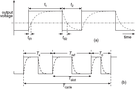
Figure 10.4 Various types of output signals (a) duty-cycle modulation (b) aperiod modulation
For example, when the smart temperature sensor SMT [16] is supplied with a voltage VDD, the averaged output voltage Vaverage amounts to
in which MSMT represents the duty cycle, which is linearly related to the temperature. This voltage is connected to one of the comparator input terminals.
The other comparator input terminal is connected to a resistive divider, which is used to control the set-point. The divider output voltage Vsetpoint equals:
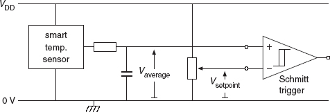
Figure 10.5 A simple electronic circuit for a temperature detector. The average value of the duty-cycle-modulated signal is compared with output voltage of a resistive divider. With the potentiometer the temperature is set at which the comparator changes it output
When the temperature measured with the temperature sensor crosses a value, for which it holds that MSMT = Msetpoint, then the Schmitt trigger inverts its state. The hysteresis of the Schmitt trigger is chosen to be larger than the ripple at the input signals, which eliminates the effect of oscillation or multi-triggering of the output voltage. The output signal can be used to control a switch that, for instance, triggers an alarm circuit, or switches on a heater in a thermostat. In this way, the potentiometer is used to control the set-point at which the comparator switches to another output state. Note, that in addition to its simplicity, duty-cycle modulation has another interesting advantage: because both values Vaverage and Vsetpoint are proportional to VDD, the set-point value Msetpoint of the resistive divider is independent of the supply voltage VDD.
Usually sensors with a duty-cycle-modulated output voltage are read out with a timer in a microcontroller. In that case, a problem could arise when such a sensor is connected with a long cable to the timer circuit. Because of the cable capacitance and the sensor output resistance, the 0–1 and 1–0 transients in the sensor signal might be too slow (Figure 10.4(a)). This will cause a time error that will depend on the threshold level of the timer and which might be different for rising and falling edges. There are solutions to this problem, such as using a buffer amplifier, using optical modulators/demodulators, or using period modulation.
Period modulators
In period modulators, the sensor information is converted to the full length of one or more periods (Figure 10.4(b), see also Chapter 2, Section 2.4). In this case, the time intervals are measured using only one type transient: the rising or the falling edge. In case of a large time constant, there will be some time delay in the detection moment. These delays are equal for all detected transients, so that their effect on the measured time differences (intervals) is compensated.
Pulse modulators
In the time domain, the output signal of an asynchronous converter is analog. Each signal sample requires a full period time. Therefore, such a time-modulated signal can considered as sampled analog signal, where a new sample is available at the end of each period. The time intervals between the signal samples are equal to an integer number of periods. When the period time is signal dependent, then the samples are not time equidistant. Usually, this does not pose a problem. However, when time-equidistant samples are required, pulse modulation can be applied. In this case the sensor signal is converted to, for instance, a time interval t1, while the period time tp is fixed.
10.3.4 Quantization Noise of Sampled Time-modulated Signals
With a microcontroller the various time intervals, t1, t2 and/or the period time tp (= t1 + t1) of a time-modulated signal (Figure 10.6) can easily be digitized. For this purpose, the output-voltage line of the asynchronous converter is connected to a timer input of the microcontroller. At the first sampling moment, after an up-going or down-going edge of the signal, the contents of a fast-running timer are copied to a special register (the capture register). In this way, time moments and time intervals are converted into integer numbers of counts. In between two sampling moments, within the sampling period ts exact information about the precise moment of the transient is lost.
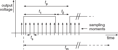
Figure 10.6 Sampling moments with time intervals ts during a total measurement time tm of a time-modulated output signal
This loss of information is similar to the loss of information in any other type of A/D converter and gives rise to a conversion error, which is called sampling error or quantization error. Averaging the result of the measurement over a large number of periods will significantly reduce this type of noise. For period modulation, this averaging process is more effective than for duty-cycle modulation. This can be explained as follows:
(a) With period modulation, after a series of concatenated periods, only the very beginning and the very end of the counting interval will introduce uncertainties. Therefore, the relative effect of the quantization error will go down proportionally to the total number N of periods.
(b) With duty-cycle modulation, any up-going and down-going edge will introduce uncertainty. When these edges are not synchronized with the sampling moments, the quantization noise contributions of the various transients are stochastically independent. Then, in the average, the quantization noise will go down with the square root of the number of counts. Care should be taken to avoid that sampling pulses of the microcontroller do not cause undesired synchronization of the sensor signal. Undesired synchronization would change the stochastic errors into systematic ones, which will exactly be repeated, each period. In that case, increasing the number of periods will not help to reduce the relative error. Injection of noise or pseudo noise can help to avoid undesired locking [17]. Averaging over N concatenated periods will yield a total measurement time tm which equals
The quantization noise has a uniform distribution function. In case of duty-cycle modulation, this noise causes a relative error with a standard deviation σq,dcm that equals

Often resolution is expressed in term of bits. In that case, the resolution Rbits is related to the standard deviation σ as:
Often, for ADC converters the resolution is specified for three or six times the standard deviation. This will yield resolution figures being 1 or 2 bits less. For comparison with other publications, in this chapter we will use resolution figures as defined in Equations (10.5) and (10.6).
In case of period modulation, quantization noise causes a relative error with a standard deviation σq,pm that equals:
For both types of modulation, using a fast microcontroller will significantly reduce the quantization noise.
Example 10.4: Quantization noise for a sampled duty-cycle-modulated signal. In Section 7.5.1, Example 7.7 refers to a smart temperature sensor with a duty-cycle-modulated output signal, where the measurement time tm = 30 ms and the period time tp = 0.3 ms. In addition to that, for this example we suppose that the sampling time ts = 0.3 μs, which represents a typical value for microcontrollers of the type 8051. According to Equation (10.5), it is found that σq,dcm = 4.1 × 10⁻⁵, which corresponds to a resolution of −(2log σq,dcm) = 14.6 bits.
Nowadays, microcontrollers can be much faster (see Chapter 12). For instance, with microcontrollers of the type LPC2101, with a clock frequency of 11.7 MHz, the internal sampling frequency is as fast as 70 MHz, so that ts = 14.3 ns. With such a microcontroller, for the same measurement conditions, the quantization noise would be reduced to only σq,dcm = 1.95 × 10⁻⁶, which corresponds to a resolution of 19 bits.
Example 10.5: Quantization noise for a sampled period-modulated signal. Suppose that the asynchronous converter would generate a period-modulated output signal. With the same data as in Example 10.4: tm = 30 ms, tp = 0.3 ms and ts = 14.3 ns (70 MHz), with Equation (10.7), it is found that σq,pm = 0.2 × 10⁻⁶, which corresponds to more than 22 bits. Such a resolution is close to that mentioned by Quiquempoix et al. [7] for a third-order incremental sigma–delta converter.
From Equations (10.5) and (10.7), it is found that σq,dcm/σq,pm = √N. This explains why, for a measurement with N = 100 periods, period modulation has a 10 times better resolution than duty-cycle modulation.
Example 10.6: Quantization noise in relation to thermal (white) noise. Figure 10.7 shows the noise in the measurement for a sensor resistor R (= 100 Ω), as measured with the universal interface presented in Chapter 2, Section 2.6. The four graphs represent the results for various values of measurement time tm and sampling time ts.

Figure 10.7 Noise of an interface system at various measurement times tm and sampling periods ts: (a) tm = 14 ms and ts = 200 ns; (b) tm = 112 ms and ts = 200 ns; (c) tm = 14 ms and ts = 14.2 ns; (d) tm = 112 ms and ts = 14.2 ns
In Figure 10.7(a) the effect of quantization noise can easily be recognized. With increasing measurement time (Figure 10.7(b)) the quantization noise decreases significantly. Equation (10.7) shows that an increase of the measurement time by a factor eight should result in a decrease of the standard deviation by also a factor of eight. However, at tm = 112 ms, the thermal noise dominates over the quantization noise, so that the reduction is only a factor of five. When the sampling time is reduced to 14.2 ns (Figures 10.7(c) and (d)), the graphs show that there is no significant quantization noise. Thermal noise is inversely proportional to √tm. Therefore, increasing the measurement time by a factor of eight (graphs (c) and (d)), decreases the standard deviation with a factor of about 2.9.
Note that systems in which thermal noise dominates over quantization noise cannot be improved by using an A/D converter with a higher resolution. For this reason a sensor systems with a 24 bit A/D converter seldom shows a 24 bit resolution (see also Problem 10.4 at the end of this chapter).
The values of the standard deviations of the measured noise signals shown in Figure 10.7 are listed in Table 10.2.
Table 10.2 Standard deviation σR in the relative value of (ΔR/R)

10.3.5 A Comparison between Asynchronous Converters and Sigma–delta Converters
Both asynchronous and sigma–delta converters belong to the group of indirect A/D converters, with as key characteristic the use of an intermediate time-domain signals in A/D conversion processes for signals in the low- and intermediate frequency range. The attractive features of indirect converters concern their high resolution, low power consumption and simplicity. Therefore, indirect converters are highly suited for smart sensor systems. The basic block diagrams of asynchronous and sigma–delta converters show a strong similarity (Figure 10.8).
In asynchronous converters, the microcontroller (Figure 10.8(a)) takes care of digitizing, using a clocked gate and a fast-running timer. Generally, to reduce power dissipation and emission of disturbing signals, it is advised to limit the application of high-frequency signals to a limited space/area. In the setup of Figure 10.8(a), the timer clock is used only within a small area at the microcontroller chip, without external wiring or connections and far away from the sensitive input amplifiers. Therefore, a very high timer frequency can be applied. As shown in Example 10.4, this results in (very) low quantization noise.
In sigma–delta converters, the clocked gate is within the feedback loop. The advantage is that the output signal is already digitized (Figure 10.8(b)), which usually will be appreciated by the user. Furthermore, when applying higher-order converters, the quantization noise and/or the clock frequency can highly be reduced.

Figure 10.8 Block diagrams indirect A/D converters: (a) asynchronous converters, (b) synchronous (sigma–delta) converters
However, with sigma–delta converters also a number of problems can arise:
- The occurrence of dead zones [9]. Practical integrators will show some leakage. Dependent of the amount of leakage, at specific dc values of the sensor signal, the resolution can drop significantly. Consequently, the worst-case resolution will drop. For the large group of sensing elements that generate low-frequency or dc output signals, this problem should be taken into account.
- Multiplexed sensing elements. To perform autocalibration or to select elements from a sensor array, at the input of the sensor system, the sensing elements are multiplexed. This causes the problem that at the beginning of each conversion the memory elements, including all of the capacitors, have to be reset. This would have the drawback of an increased acquisition time, thus slowing down the operation speed of the sensor system. The use of special filter topologies and initialization circuits (feed-forward paths) [9]. can solve this problem and speed up the conversion rate.
In ref. [9]. many examples can be found of sigma–delta converters that have been designed for smart temperature sensors. It has been shown that such circuits can be combined with other circuits, which are needed for, for instance, calibration of reference purposes. In ref. [7]. a third-order incremental converter is presented, implemented in 0.6 μm CMOS technology. The ADC chip contains also an internal programmable oscillator, a decimation filter and a bus interface. With a clock frequency of only 30 kHz, a resolution of 22 bits is obtained for a conversion time of 67 ms.
When using a microcontroller with a fast timer (see Example 10.5), with asynchronous converters a similar performance can be obtained. In this case, the excellent properties of the asynchronous converters are due to the very high sampling frequency in the microcontroller timer. These high frequencies are only found locally in a limited area and volume of the microcontroller chip. In this part of the chip, power consumption can be limited by minimizing the parasitic capacitances and by using a reduced supply voltage. Related to this, possible undesired effects of interference and cross-talk can also be limited. Always, limiting the spatial volume of EM fields is an effective way to reduce possible problems of high-frequency signal processing.
The simplicity of asynchronous converters is because they concern a first-order system and because the quantization process is performed in the microcontroller. Furthermore, the very limited number of internal memory cells allows rapid adaptation of the converter to changes in the front-end circuit, or to multiplexing of sensing elements, or to change the acquisition time. It is possible to make asynchronous converters with a built-in quantizer, so that a digital output signal is achieved. However, then the advantage that no counter, external clock line or internal clock is needed, is lost.
In summary, it can be concluded that asynchronous converters have the attractive features of simplicity and flexibility for rapid changes in the front-end circuitry or in the signal processing. These features make these converters attractive for universal converters with many front ends and many users’ options. Because of the small chip size, integrated asynchronous converters can easily be combined with sensing elements as a system in a package. Moreover, because of their simplicity, asynchronous converters are rather suited for low- and medium-volume applications. In such applications, a universal interface can perform multiplexing, chopping and precision analog processing of the sensor signal, while a low-cost microcontroller performs quantization and digital signal processing.
On the other hand, sigma–delta converters offer the advantage of delivering a digital output. For high-volume applications the complexity of sigma–delta converts is not a big problem, which makes these converters rather suited for dedicated designs of smart sensors and systems on a chip (SOCs) with embedded microcontrollers.
10.4 Dealing with Problems of Low-cost Design of Universal Interface ICs
For users of universal interfaces it is helpful to understand the trade-offs to be made by designers of universal integrated circuits. This will help them to understand the limitations of present designs and to discover possible opportunities for making improved dedicated designs. The main drive behind the development of universal chips is the wish to offer low-cost high-volume products for the small- and medium-volume market. Designers and producers of universal interface chips have to take care to optimize the number of modes. From one hand, because of the higher production volumes, it can be an advantage to have a large number of modes for a very wide range of possible applications. For the user this could be attractive, because he can reuse his knowledge and tools for various applications. On the other hand, a too large a number of modes will increase the testing costs (see below) and will also increase the complexity for the user. Therefore, it will be more attractive to have a family of chips, with different members for various sensor groups. Each of them being users friendly and fabricated at low costs.
In case of sensor-interface chips, the cost ingredients are related to the costs of:
- Integrated Circuits. The die (chip) costs are proportional to the chip size. In CMOS technology the chip size can be much less than in, for instance BICMOS technology. In case of small circuits, shrinking of the chip size is limited by the number of bonding pads. Therefore, CMOS technology and architectures with moderate number of bonding pads will be favorable.
- Packaging. Small packages will be attractive to limit costs and size of the sensor systems.
- Testing. Testing costs can make up a considerable part of the total chip costs. In universal systems, a large number of tests have to be performed, to check the functionality and quality of the various front-end circuits. The specific users will only be interested in a few of the available modes and does not want to pay for unused options. This limits the optimum number of modes for each member of the interface family.
The use of CMOS technology introduces some specific problems for the design of precision front-end circuits. These problems and their solutions are:
- Mismatching of components. This will cause a large offset-voltage of the input amplifiers and also cause (systematic) inaccuracy of transfer functions. As explained in Chapter 2, these problems can be solved by applying autocalibration, chopping and dynamic element matching (DEM).
- Excessive low-frequency (1/f) noise. This is because CMOS transistors are surface devices, where the main currents flow along the irregular Si–SiO2 interface, instead of through a perfectly-shaped bulk crystal. This problem can be solved by applying chopping and autocalibration (see Chapter 2). The chopper should modulate the desired signal and convert it to a frequency higher than the noise corner frequency. Afterwards, the desired and undesired signals are separated using appropriate filters. With an output chopper, the original signal is restored. For noise frequencies below the autocalibration rate, in addition to the chopper action, also autocalibration helps to reduce noise.
- Switching effects. To apply the techniques mentioned above, in the sensitive parts of the front-end circuitry many switches are used, which introduce problems to be discussed in the next subsection.
10.5 Front-end Circuits
10.5.1 Cross-effects and Interaction
The front-end circuits are very important, because they have to act as converters with optimum adaptation to the sensing element and the A/D converter, at input side and the output side, respectively. Often the sensing elements acquire physical information under difficult physical circumstances. Therefore, as discussed in Chapter 2, Section 2.3, for selective signal processing also the nonidealities of the sensing elements have to be taken into account. These nonidealities will include physical cross-effects, noise, interference, electrostatic discharge (ESD), impedance levels, etc. To cope with these problems, even in a universal sensor interface, the front ends are not universal at all. Instead of this, front-end circuits are tailored to have optimal features for specific tasks. This is accomplished by applying the best measurement techniques (Chapter 2) and, in addition to this, by using high-quality components. In front-end circuits, the electronic properties of the interface interact with those of the environment. This can cause undesired physical, chemical and electrical effects in both parts of the system.
Example 10.7: Undesired interaction
Chemical effects: A dc biasing input current or excitation voltage generated by the interface can cause chemical problems, including corrosion, of the sensing element. Also the use of a switched-capacitor (SC) input of the interface will cause some dc current, which flows through the sensing element.
Physical effects: An excitation current for a resistive temperature sensor can cause undesired heating of the sensitive element.
Electrical effects: The decision to connect or not to connect sensing elements to ground can easily affect the biasing conditions of an input amplifier in a front end.
In addition to these measures, the properties of the interface circuit can be improved by minimizing the systematic and random errors of the interface and the connecting wires, as will be explained in the next subsection.
10.5.2 Interference
In high-resolution sensor systems, noise and interference should be kept as low as possible, to minimize the stochastic errors. As a first step, thermal noise can be reduced by optimizing filter characteristics for the best signal-to-noise ratio of the front-end circuit. As a next step, the resolution can be improved with an increase of the measurement time. As shown in Section 10.3.4, for period-modulated signals, quantization noise reduces inversely proportionally to the measurement time, while thermal noise reduces inversely proportionally to the square root of the measurement time.
In addition to noise reduction, it is very important to design for a high immunity to interfering signals. Shielding of connecting wires at the interface input should reduce the interfering signals as much as possible. However, to function properly, sensing elements have to interact with their environment, which limits the possibilities of taking proper measures against electromagnetic interference. Therefore, it is advised where possible to use interference filters in the connecting wires. For low-frequency disturbing signals, filtering can be realized by autocalibration and chopping. In Section 10.6.1, for capacitive sensor systems, some theoretical and experimental results have been presented.
To suppress high-frequency disturbing signals, good low-pass filtering is required. Interference of the microcontroller clock can cause undesired locking of the oscillator signal to the microcontroller clock frequency. In that case, over a wide range of periods the quantization errors are repeated in exactly the same way, so that a reduction of quantization noise cannot be obtained by averaging over a number of periods. To eliminate this effect, in addition to filtering of clock-feedthrough signals, dithering techniques can be applied [10, 17] to disable locking.
10.5.3 Optimization of Components, Circuits and Wiring
At the interface site of the sensor system, systematic errors can be reduced, for instance, by optimizing the features of the following components and circuits:
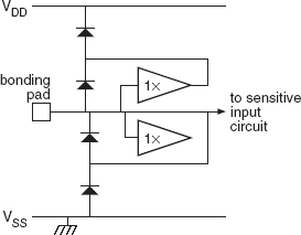
- Protection circuits. These circuits protect the chips against electrostatic discharge and contain protection diodes. For sensor application, possible problems of these diodes concern their temperature-dependent leakage current and their internal capacitances. Sensing elements, such as thermopiles and pH sensors, can have a rather high internal resistance. The product of resistance leakage current results in an equivalent voltage error, which limits the accuracy. Special low-leakage circuits for ESD protection should be applied (Figure 10.9). When connecting, for instance, capacitive sensors, the effects of the parasitic capacitances have to be taken into account. In smart temperature sensors and smart acceleration sensors, the input signals are physical instead of electrical. This makes protection much easier. This is one of the advantages of implementing a sensor and its interface as a smart sensor.
- Switches. Switches are used to select specific sensing elements, and to connect them with the most appropriate input circuit. They are also used as choppers, to convert dc sensor signals to ac signals. Electronic switches have parasitic diodes, which introduce leakage currents and parasitic capacitances similar to those mentioned for the protection diodes. Fortunately, optimization of the size and lay-out of the switches enables the magnitude of these nonidealities to be reduced. For choppers, at the dc side of the switches minimization of leakage currents is important, while at the ac side time constants have to be minimized. The size of the switches in discrete off-the-shelf multiplexers is often large. The manufacturers of these switches have made this choice in order to reduce the switch ON resistance. However, a large switch size has the disadvantages of a high leakage current and large capacitance. For specific front ends, with dedicated designs, for each switch the best compromise can be found. For switches used for precision charge transfer, the effects of clock-feedthrough and channel-charge injection have to be minimized. Also in this case optimizing the switch size is a good start for optimizing the front-end performance. As a next step, switching effects can be reduced by appropriate timing of the mutual ON/OFF sequence of the various switches, using nonoverlapping/overlapping switch control signals. Finally, especially for low-frequency sensor signal, compensation of switching effects can be realized with autocalibration and nested-chopper techniques (see Chapter 2, Section 2.5.2)
Figure 10.9 Principle of a bonding pad with active guarding with low-leakage ESD protection
- Capacitors. Capacitors are used for filtering, for charge transfer in switched-capacitor (SC) front-ends, and for dc decoupling. In the latter application, these capacitors have to prevent that the connections of external sensing elements disturb the biasing conditions of the front-end amplifiers. In IC technology, there is a wide variety of capacitors available. Important capacitor properties concern: the capacitance per unit of chip area, the breakdown voltage, the nonlinearity (voltage dependence), the leakage current or charge loss, and the parasitic capacitance to the substrate (GND). With metal or polysilicon electrodes and high-quality oxides, excellent capacitor features are achieved. In today's IC technology many metal and polysilicon layers are available. Some of these layers can be used for shielding or guarding purposes (see also Chapter 8), which can improve immunity for interference and surface effects.
- Amplifiers and dividers. In the front-end circuits, amplifiers and dividers are used to amplify or to reduce the size the signals, thus reducing the required dynamic range of the signal processors (see Chapter 2, Section 2.5.4). As mentioned before, typical problems of these circuits, which are mainly related to poor component matching and low-frequency (1/f) noise, can be solved by applying chopping, DEM and autocalibration.
10.6 Case Studies
10.6.1 Front-end Circuits for Capacitive Sensors
As a first case study, we will compare and discuss the architectures and properties of various interfaces for capacitive sensors that have earlier been presented in Chapters 2, 8, and in Section 10.3 of this chapter. In Chapter 8, Section 8.6.3, an interface circuit (Figure 10.10) has been presented, that generates a square-wave output signal which is proportional to the sensor capacitance Cs.
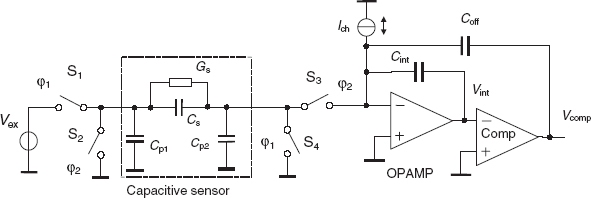
Figure 10.10 Direct use of the charge-to-time converter as interface by using the capacitive sensing element Cs as sampling capacitor
The basic principle of this circuit is similar to that of the charge-to-time converter presented in Figure 10.2. In Sections 10.3 and 8.6 it has been explained that the sensor capacitor is used as a sampling capacitor and that the circuit has the attractive feature that when the sampling capacitor is discharged rapidly, the effect of a shunting conductance Gs is reduced. This makes this configuration rather suited for sensing elements with leaky capacitors, such as capacitive humidity sensors. However, when the sensing capacitors have a small value, then the signals can be too small to take full advantage of the large dynamic range of the charge-to-time converter. Especially in universal interfaces, the charge-to-time converters should be able to be operated over a large range, to enable a wide variety of applications. Usually, such a universal converter does not show the optimum performance to be connected directly to a sensing element. For instance, in the universal transducer interface (UTI) presented in Chapter 2, Section 2.6.1, the charge-to-period converter is preceded by a dedicated front-end amplifier (Figure 10.11). Because this amplifier has been designed for just one type of sensing element, its noise performance can be optimized for this application. This explains that, even for sensor capacitors with a full-range value of only 2 pF, still a very high resolution/repeatability of 50 aF (Table 2.1) can be obtained. However, the user should realize that with an excitation frequency in the range of (50 to 100) kHz the sensor impedance is very high, so that even a small shunting conductance will have a large impact for the resolution.

Figure 10.11 Principle of the UTI system for capacitive-sensor modes
Example 10.8: It can be shown (see the solution to Chapter 2, Problem 2.2), that for the interface circuit of Figure 10.11, a shunting leakage conductance Gleak of sensor capacitor Cx will cause a relative error εsh in the measurement, which equals:
From this equation it can be calculated that, for Cx = 2 pF and (t2 − t1) = 10 μs and an error smaller than 500 aF (εsh = 0.25 × 10⁻³), it should hold that: Gleak < 2 × 10⁻¹⁰ S!
Example 10.8 shows that for high-precision capacitive sensors the occurrence of shunting conductance should be avoided. Therefore, such sensors should be applied in a clean environment. When this is not possible, because of its lower sensitivity for shunting conductance, application of the circuit of Figure 10.10 would be a better option. In both circuits, the use of the advanced chopping technique (Chapter 2, Section 2.5.2) suppresses interfering signals at the input of the sensing element. In fact the interface circuit, which generates the excitation signal and detects the responding signal of the sensing element, acts as a synchronous detector (Figure 10.12) [18].
The high-pass filter (HPF) represents the action of the advanced chopping technique. As explained in Chapter 2, Section 2.5.2, the filter transfer function is given in the z-domain by:
Substitution of z = exp(jωTmod), Tmod being the modulator period, will transform Equation (10.9) into an expression in the frequency domain, which shows that the filter has a second-order frequency filtering for low frequencies of the interference. In an experimental setup for capacitive sensors [18] test results on the suppression of low-frequency interfering signals have been reported. In an experimental setup a test voltage that simulates the interference was capacitively coupled to input A (the common electrode at the left-hand side in Figure 10.11). The coupling capacitor was as large as the sensor capacitance Cx. The relative interfering amplitude equals the ratio of the amplitude of the interference and the amplitude of the signal on the transmitting electrode (VDD/2). Figure 10.13 depicts the experimental results together with the calculated ones found with Equation (10.9), which appear to be close to each other.
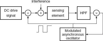
Figure 10.12 Principle of the interface system for capacitive-sensor modes

Figure 10.13 Suppression of low-frequency interfering signals for capacitive measurements with the system of Figure 10.11
10.6.2 Front-end Circuits for Resistive Bridges
The second case study concerns a front-end circuit for a resistive-bridge sensor. Such sensors are frequently used in mechanical sensors for measuring force, pressure, acceleration etc. In many traditional interface circuits for resistive bridges, reference voltages are applied as a dc excitation source. The same or another dc reference source is used to perform precise measurement of the bridge-output voltage Vo (Figure 10.14), where it holds that
where εbridge is the relative bridge imbalance, Rbridge is the bridge resistance, and Vs and Is the bridge supply voltage and current, respectively.
Sometimes, instead of a reference supply voltage Vs, a reference supply current Is is used. The difference is that in this case the output voltage is also proportional to the bridge resistance, which is temperature dependent. Some manufacturers of sensor gauges use this temperature dependence as a low-cost way to compensate for opposite temperature effects of, for instance, mechanical effects in their gauges. Of course, it would be a better approach to measure the temperature and to perform temperature compensation in an algorithmic way in, for instance, a microcontroller.

Figure 10.14 Resistive bridges with voltage supply or current supply
From Equation (10.10) it can be concluded that it is not necessary to use (expensive) references sources. Since the relative bridge imbalance εbridge represents the measurand, a ratiometric measurement of Vo and Vs or of Vo and Is will be more precise. In that case, stability of the supply voltage is only required over the short measurement time interval, which is in the order of tens of ms.
Another drawback of the traditional setup is that it uses a dc supply voltage. This is often not allowed, because it can cause corrosion, thus reducing the lifetime of the sensor gauge. Moreover, many signal nonidealities, such as offset, parasitic Seebeck voltages, and 1/f noise, are also in the low-frequency range. Therefore, often ac supply voltages are preferred.
These problems are solved in the universal sensor interface presented in Chapter 2. In Figure 2.23 of that chapter, the system setup has been presented, which is shown in more detail in Figure 10.15. The interface circuit consists of:
- an excitation part which generated an ac bridge-supply voltage/current;
- a divider part to measure the bridge-supply voltage/current;
- a selector, which selects the various voltages to be measured;
- a DEM amplifier to amplify small output voltages;
- a voltage-sampling circuit;
- a universal charge-to-time converter.
The excitation signal is derived from the supply voltage, using a pair of chopper switches S1 and S2, which can invert the supply voltage, thus generating a square-wave bridge-supply voltage with amplitude VDD (and peak-to-peak value of 2VDD!).
The switches are controlled by the relaxation oscillator in the charge-to-period converter. This is an interesting feature: Although the interface is asynchronous with respect to an external clock, internally it is synchronized by the oscillator signal, which period also represents the measurand. The importance of this feature is that in this way it is possible to apply synchronous detection as shown before in Figure 10.12, and enabling filtering of low-frequency interference as described for the capacitive sensors.
For the output voltage Vout optionally an amplifier can be used. In case that no amplifier is used, the bridge output voltage is sampled with the four sampling capacitors Cs,1–Cs,4 connected in parallel. Next, the sampled charge is transferred to the charge-to-period converter. For an accurate ratiometric measurement of Vo/Vs, the same sampling capacitors should be used for sampling the bridge supply voltage Vs. Because of the high value of the supply voltage, this voltage is split up into smaller parts, which are more close to the size of the output voltage, but do not have to be exactly equal. This action is performed with the resistive divider R1–R8 and the corresponding switches. The voltage across each of the resistors is sampled by one of the capacitors Cs,1–Cs,4. After a complete cycle of 32 samples, each of the eight voltage parts has been sampled by each of the four capacitors. The results of all of these submeasurements are added in the microcontroller. In this way, the sampled supply voltage is measured part-by-part with the same sampling components as the output voltage. This equalization of the size of the charge samples, results in much more relaxed requirements for the dynamic range of the charge-to-period converter.
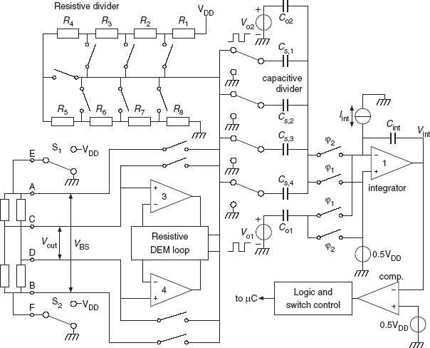
Figure 10.15 Setup of a bridge interface circuit
When an amplifier with gain A is used, following the same procedure, the ratio AVo/Vs is measured. Therefore, the amplification factor A should be known very precisely. This can be achieved by applying an amplifier with dynamic element matching (DEM) as described in Chapter 2, Section 2.5.4.
To complete the method of three-signal autocalibration, in each measurement phase an offset measurement is also performed. During the offset measurement the sensor signal is zeroed. To compensate as well as possible for circuit nonidealities, including switching effects, the offset measurement is performed by sampling a zero-voltage difference, for instance, at the CM level of VDD/2. In the ideal case, the magnitude of the common-mode voltage should not make any difference. However, in practice there are some differences, which are due to the common-mode dependence of nonidealities. Therefore, to optimize the precision of the measurements, for each of the relevant CM levels, an offset measurement should be performed. This will have the drawback of an increased measurement time. To overcome this drawback, the number of offset measurements can be reduced by performing them one by one, over a longer series of measurements. In the microcontroller it will not be difficult to handle the larger series of data.
In Figure 10.15 two offset capacitors C01 and C02 have been indicated. The offset capacitor Coff1 is used to create time intervals for capacitors Cs,1–Cs,4 to sample the voltage to be measured. During this sampling time, the signal voltages are converted into charge in the capacitor Cs,1–Cs,4. In the next subphase of a measurement cycle this charge is transferred to the integrator capacitor Cint. Together with the comparator and control switches a charge-controlled relaxation oscillator is formed that linearly converts the voltages into periods of the oscillator output signal. The second offset capacitor Coff2 is needed to enable negative values of the thermocouple voltages. More details concerning the applied signal processing techniques in this circuit can be found elsewhere [19].
10.6.3 A Front-end Circuit for a Thermocouple-voltage Processor
As a third case study, we will discuss a front-end circuit of a measurement system for thermocouple signals. Thermocouples generate small output voltages which, depending on the type, are in the range of (5 to 40) μV K−1 (see Chapter 6, Table 6.3). For a measurement accuracy of, for instance 0.5 K, the inaccuracy of the thermocouple interface should be less than an equivalent input value of a few tens of microvolts.
With thermocouples the temperature difference between, at least, two junction temperatures is measured. To measure an absolute temperature, it is necessary to measure also the temperature of the reference junction(s), with for instance a thermistor or a smart temperature sensor (see Chapter 7). The inaccuracy of this measurement should be equal to or less than that of the thermocouple-voltage.
Of course, for such a precise measurement, autocalibration should be applied. In addition to the measurement of the thermocouple voltage VX and the reference-junction temperature TJ, this will require the measurement of a reference voltage Vref and an offset voltage Vos. So with these measurements, at least four measurements have to be performed. For the reference voltage, an external reference source can be applied. However, as an interesting alternative, the principles of transistor sensors (Chapter 7, Section 7.4.4) can be applied for both the generation of the required reference voltage and the measurement of the reference-junction temperature. This measurement principle has been applied in the system shown in Figure 10.16 [20]. This system is implemented with an interface chip in which the base–emitter voltage VBE of a bipolar transistor and the PTAT voltage VPTAT = ΔVBE are used to generate both the reference voltage and the temperature-sensor voltage. The various voltage sources and the offset voltage are selected with the multiplexer switch. In the lower position of the switch the offset voltage VOS is measured. In total, four basic signals, VX, VBE, ΔVBE and the offset voltage VOS are measured. These voltages are converted to the time domain by a linear voltage-to-period converter, which is operated in a similar way to the charge-to-period converter discussed in the previous case study (Section 10.6.2). When the output periods during the successive measurements are tX, tBE, tPTAT and tOS, respectively, then the final result FV for the thermocouple-voltage measurement amounts to:

Figure 10.16 Basic setup for a dynamic voltage measurement system
The final result FV is independent of the multiplicative and additive errors and parameters of the converter. In a similar way, with the three periods tBE, tPTAT and tOS, the chip temperature can be calculated. In the microcontroller, the algorithmic signal processing, including adding, subtracting, division and nonlinearity correction is performed. Also data storage and data processing is performed in the microcontroller. The microcontroller (Figure 10.17) measures the each phase duration and calculates the ratio F using Equation (10.11) and with a similar equation also the chip temperature.
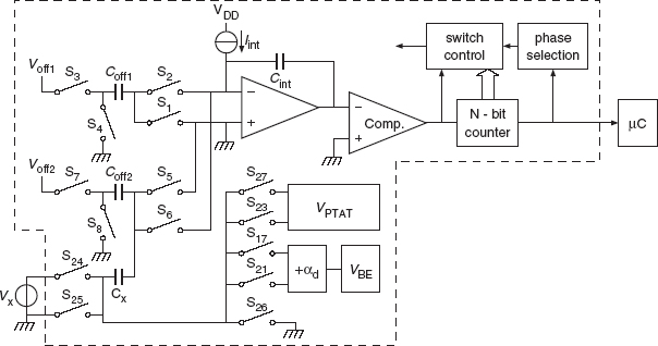
Figure 10.17 Schematic diagram of a system for dynamic voltage processing
The tested chip shows a standard deviation of 8 μV for the voltage measurement and 50 mK for the temperature measurement, for a measurement time of 50 ms. For the voltage measurement a relative (scale) error of −550 × 10−6 is reported.
10.7 Summary and Future Trends
10.7.1 Summary
In this chapter it is shown that, for the medium- and low-volume markets, universal sensor interfaces enable rapid prototyping of low-cost, high-performance sensor systems. The output signals of the interface chips can be digital or time-modulated, so that they can be read out by microcontrollers. Attractive features of generating digital signals concern the easy way of data processing, where for high-volume products, a high complexity and a low flexibility of circuits is not a main problem. This chapter deals with systems in which time-modulated signals are applied. Attractive features of such systems concern the simplicity of the circuits and the flexibility of the signal processing. For use in sensor systems, such features are important with an eye on a reduction of power consumption, and to enable immediate adaptation to multiplexing of the sensor elements.
Time-modulated signals can easily be generated with asynchronous converters, which can be implemented with relaxation oscillators. The application of faster microcontrollers reduces the level of quantization noise of the sensor system, which are suited for acquisition ranges up to a few kilohertz. When using a microcontroller with a 70 MHz counter, for an acquisition rate of 1 kHz, systems with asynchronous converters can show a resolution of better than 12 bits. The application of integrators with negative feedback can improve the resolution with one or two bits.
The universal sensor-interface chips can be implemented with low-cost CMOS technology. Because of the smaller transistor dimensions, circuits implemented in CMOS technology are much smaller than those implemented in BICMOS or Bipolar technology. The typical drawbacks of CMOS technology, such as 1/f noise and component mismatching can be overcome by applying autocalibration and dynamic element matching (DEM).
To make users-friendly interface circuits, the interface-chip designer has to deal with the specific physical measurement problems. To cover a wide range of applications, a range of dedicated front-end circuits is required for a number of typical applications. The use of dedicated measurement techniques, including autocalibration, two-port measurement and advanced chopping, is important to make the chips easy to use. Moreover, the mentioned techniques enable selective detection of the measurand with a high immunity for parasitic effects of the sensing elements, and for the effects of the connecting wires. By applying synchronous detection, autocalibration and advanced chopping also high immunity is obtained for interfering signals, 1/f noise and parameter drift. As case studies, the design details and features of interface circuits and systems have been presented for capacitive sensors, resistive-bridge sensors and thermocouple-voltage processors.
10.7.2 Future Trends
Only recently has the introduction of sensor interface products been started. These interfaces have a high added value for a wide range of industrial and commercial products. The application of these low-cost products will cause acceleration of ‘sensorization’ of our society. Because of their low costs, advanced sensor systems will soon be found in consumer products, games and toys, thus changing everyday life style.
Universal devices are attractive for products with a small- and medium-volume market. However, for higher product volumes, universal products have the drawback that the user pays for unused options. Therefore, it is expected that soon sensor-interface products will be offered in large families, with many chip members for specific tasks. The use of multi-chip packages will enable to use the best technologies for each of the system parts.
Problems
10.1 Charge-to-time converter (see Section 10.3.1)
Figure 10.18 shows the integrator part of the signal-to-time converter, earlier presented as Figure 10.2. The reference current source has an internal resistance RCS, which affects the period time and the duty cycle of the output signal. The supply voltage amounts to VDD = 4 V, RCS = 10 MΩ and Iref = 1 μA.
Answer the following questions:
(1) How large is the duty cycle of the output signal?
(2) How large is the period time tp of the output signal when the capacitor CS (Figure 10.2) is measured and when Vx = VDD?
10.2 Charge-to-time converter (see Section 10.3.1)
Consider the SC front-end circuit of Figure 10.3 and answer the following question: What is the magnitude of the current iCs during the time interval t1 to t2?
10.3 The effect of time constants for a duty-cycle-modulated signal (see Section 10.3.3)
The duty cycle of a square-wave signal V1 (Figure 10.19(a)) is to be measured. However, internal resistance R = 1 kΩ and the cable capacitance C = 1 nF cause the output signal V2 at the input of the counter to have the shape depicted in Figure 10.19(b). The time intervals are derived from the moments that V2 crosses a threshold value Vthres. Answer the following questions:
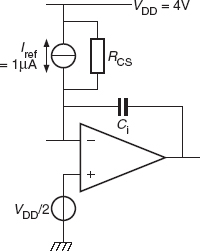
Figure 10.18 The integrator part of a signal-to-time converter
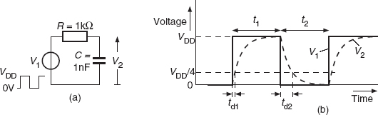
Figure 10.19 A duty cycle voltage generator with its internal resistance and parasitic capacitance of a connecting cable. (a) Equivalent circuit diagram; (b) output signal
(1) How large are the time intervals td,up and td,down for the case that Vthres = VDD/4 and t1 = t2 = 150 μs?
(2) How large is the error εdc in the measured duty cycle, as caused by the time delays td,up and td,down?
10.4 A comparison of quantization noise and white noise (see Section 10.3.4)
Compare the graphs of the noise signals depicted in Figure 10.7 and the corresponding values of the standard deviations listed in Table 10.2. Find solutions for the following problems:
(1) When ts = 200 ns (Figures 10.7(a) and (b)), find an estimation for the value of the measurement time tm for which the quantization noise and the white noise have equal standard deviations.
(2) Figures 10.7(c) and (d) show that for ts = 14 ns, there is no significant quantization noise. However, when shortening the measurement time tm, the relative effect of the quantization noise will increase (see also Chapter 2, Figure 2.25). Calculate the measurement time tm for which the quantization noise and the white noise have equal standard deviations.
10.5 Front-end circuits for resistive bridges (see Section 10.6.2)
(1) A resistive bridge is supplied with a dc excitation voltage VS,DC = 5 V. (Figure 10.20(a)). The output voltage of the bridge is amplified with a differential amplifier, which has an offset voltage Vos = 1 mV. When the full-scale value of the bridge imbalance amounts to ±0.25 %, calculate the relative error εos caused by the offset voltage Vos.
(2) To overcome the problem with the offset voltage, the dc excitation voltage is replaced by an ac voltage VS,AC. This voltage is derived from the supply voltage with a pair of switches with an internal resistance of 100 Ω. Figure 10.20(b) shows an electrical circuit diagram of this configuration. Calculate the error εsw caused by the switch reisistors RS.

Figure 10.20 Equivalent electrical circuit diagrams of a resistive bridge system with (a) dc excitation, (b) ac excitation
10.6 Front-end circuits for resistive sensors (see Section 10.5 and Chapter 2, Section 2.3.2)
A temperature T is measured with a resistive temperature sensor Rt of about 100 Ω. The sensor resistor is connected in a four-wire configuration to a resistance meter (Figure 10.21).
Each of the wires has an internal resistance RW = 1 Ω. In attempt to reduce interference, at the side of the resistance meter, the input terminals have been short circuited, as shown in Figure 10.21. When dR/dT = 0.4 % K−1, calculate the equivalent temperature error εT caused by making these short circuits.

Figure 10.21 Equivalent electrical circuit diagram of a resistive sensor connected in a four-wire configuration to a resistance meter. In attempt to reduce interference some input terminals of the meter have been interconnected
References
[1] ERA_Technology (1994). Target Specifications of the USIC.
[2] Analog Devices (2006). www.analog.com, data sheet LC2MOS Signal Conditioning ADC with RTD excitation currents.
[3] Maxim (2006). www.maxim.com, data sheet MAX1452 Low-cost, precision sensor signal conditioner.
[4] Melexis (2006). www.melexis.com, data sheet MLX90314 High gain programmable sensor interface.
[5] Triad Semiconductor (2004). www.triadsemi.com, data sheet Universal smart sensor interface.
[6] Smartec (2006). www.smartec.nl, data sheet Universal Transducer Interface UTI.
[7] Quiquempoix, V., Deval, P., Barretto, A., Bellinni, G., Markus, J., Silva, J. and Temes, G. (2006). A low-power 22-bit incremental ADC, IEEE Journal of Solid-State Circuits, 41, 1562–1571.
[8] Jespers, P.G.A. (2001). Integrated Converters, Oxford University Press, Oxford.
[9] Pertijs, M.A.P. (2005). Precision temperature sensors in CMOS technology. PhD Thesis, Delft University of Technology.
[10] van der Goes, F.M.L. (1996). Low-cost smart sensor interfacing. PhD Thesis, TUDelft, The Netherlands.
[11] van der Goes, F.M.L. and Meijer, G.C.M. (1996). A novel low-cost capacitive-sensor interface, IEEE Transactions on Instrumentation and Measurement, 45, 536–540.
[12] Gasulla, M., Li, X. and Meijer, G.C.M. (2005). The noise performance of a high-speed capacitive-sensor interface based on a relaxation oscillator and a fast counter, IEEE Transactions on Instrumentation and Measurement, 54, 935–939.
[13] Meijer, G.C.M. and Iordanov, V.P. (2001). SC front-end with wide dynamic range, Electronics Letters, 37, 1377–1378.
[14] Heidary, A. and Meijer, G.C.M. (2007). A low-noise switched-capacitor front end for capacitive sensors. In IEEE Sensors, Atlanta.
[15] Heidary, A. and Meijer, G.C.M. (2007). An integrated switched-capacitor front-end for capacitive sensors with a wide dynamic range. In 33rd European Solid State Circuits Conference, 2007, ESSCIRC.
[16] Smartec (2006). www.smartec.nl, data sheet Temperature sensors.
[17] de Jong, P.C., Meijer, G.C.M. and van Roermund, A.H.M. (1996). A new dithering method for sigma-delta modulators, Analog Integrated Circuits and Signal Processing, 10, 193–204.
[18] van der Goes, F.M.L. and Meijer, G.C.M. (1997). A universal transducer interface for capacitive and resistive sensor elements, Analog Integrated Circuits and Signal Processing, 14, 249–260.
[19] van der Goes, F.M.L. and Meijer, G.C.M. (1997). A simple accurate bridge-transducer interface with continuous autocalibration, IEEE Transactions on Instrumentation and Measurement, 46, 704.
[20] Khadouri, S.H., Meijer, G.C.M. and van der Goes, F.M.L. (1997). A CMOS interface for thermocouples with reference-junction compensation, Analog Integrated Circuit and Signal Processing, 14, 235–248.
Smart Sensor Systems Edited by Gerard C.M. Meijer
© 2008 John Wiley & Sons, Ltd