5
Physical Chemosensors
Michael J. Vellekoop
5.1 Introduction
Sensors that apply physical effects to determine chemical or biochemical measurands have generated significant interest in the past decade. In comparison to direct chemical sensors, where chemical-sensitive films are applied, physical chemosensors and biosensors have a simpler design and easier fabrication, a lower contamination sensitivity, and better aging properties. In this chapter, an introductory overview is given of the design and application of integrated physical chemosensors and biosensors.
Several definitions of chemical sensors and biosensors can be found in the literature. The definition given by Schultz and Taylor [1] reads: ‘measurement devices which utilize chemical or biological reactions to detect and quantify a specific analyte or event’. Goepel and Schierbaum [2] say ‘chemical sensors are (miniaturized) devices which convert a chemical state into an electrical signal’. In a study by the National Materials Advisory Board [3]. chemical sensors are defined as ‘devices or instruments that determine the detectable presence, concentration, or quantity of a given analyte’. Others as well add the term ‘real-time measurement’.
Although these definitions seem similar, some distinct differences can be observed. The first one mentions the use of a chemical reaction, while the second definition talks about ‘a chemical state’. The third definition includes ‘instruments’, while the other two refer to ‘devices’. In any case, a (bio)chemical sensor contains different parts. The scheme of such a sensor is given in Figure 5.1. Molecules in a fluid (target analyte) adhere to a recognition site (the chemical or biochemical interface), which is located on a transducer. The interface consists of a selective, chemically-sensitive layer. The adherence causes a change that is converted into an electrical signal by the transducer. Interface electronics modify the transducer output into a proper electrical signal.

Figure 5.1 Schematic representation of a chemical sensor including a chemical interface
5.1.1 Thin-film Chemical Interfaces
A vast number of different transducers for direct chemical sensing have been developed and are commercially available. Some examples are: transducers using surface plasmon resonance, surface acoustic waves, sheet resistance, capacitance, calorimetry, and the chemFET. To provide these transducers with a chemical sensing function, a chemical interface is applied on top of the transducer. This interface, which is normally a thin film of a chemically active material, must meet several specifications: it must be sensitive and selective, robust, stable, and contamination-resistant, it must have a long lifetime, and it should show low aging. In addition, the fabrication process must be reproducible and cost-effective. In practice, many interfaces have been tested for sensor applications in research institutions, but the commercialization of sensors that use a thin chemical interface is hampered because of these strict requirements [4–10].
Another disadvantage of direct chemical sensing is the fact that a new chemical interface needs to be developed for every application; it is seldom a generic technique. This makes a breakthrough to commercial products difficult to accomplish because of economic reasons; the production volumes are often too low to allow for sufficient research investment.
5.1.2 Total Analysis Systems
In the early 1990s, a Swiss group initiated a new concept in the field of (bio)chemical analysis: the concept of micro total analysis systems or μTAS [11, 12]. They stated that the requirements posed on direct chemical sensors are so high, ‘that realization in the near future is hardly possible’ and suggested to combine measurement techniques from the field of analytical chemistry with miniaturization technology (microtechnology), in order to increase analysis speed and decrease the amount of sample needed for analysis. Fluid sampling, pumping, mixing, heating, selection, separation, reacting, detection, and data handling should all be done on one single chip, the so-called lab-on-a-chip. Since 1994, μTAS has been the topic of a symposium and it is acknowledged as a field of its own [see for example [13].
Meanwhile, it has become clear that, when the term total analysis system is taken too literally, the development of a commercial product is also not feasible. Integration of so many functions into one chip is, again, hardly possible. Minor parts that affect the performance of major parts produced in the same chip determine the overall quality of the system. Therefore, the integration of (bio)chemical sensors that use a biochemical interface into a μTAS device might be a risk for the functioning of the whole system. Separate components of a μTAS have been developed into products by several companies. Examples can be found on the web.*

Figure 5.2 Schematic diagram of a physical chemosensor lacking a chemical interface
Another approach towards fast chemical or biochemical sensing is the use of physical chemosensors. This will be explained in the next section.
5.2 Physical Chemosensing
We define physical chemosensors as devices that determine chemical properties of a fluid by measuring physical properties of, or phenomena in, that fluid. A chemical or biochemical interface where adsorption or desorption of molecules takes place is not required. The schematic representation of a physical chemosensor is shown in Figure 5.2. The attractive aspect of this approach is the less complex design of the sensor, which could allow commercial devices to develop dramatically faster than direct chemical sensors [14–16].
It is interesting to see that according to the definition of Schultz and Taylor, these physical chemosensors would not be called chemical sensors because a chemical or biological reaction does not take place. However, the definitions of Goepel and Schierbaum, and of the NMA Board, comprise what we call physical chemosensors.
Some physical chemosensors are selective while others are not. In the latter case, (physical) separation techniques can be applied to attain the required selectivity (Figure 5.3). Because of this pre-separation, the sensors used can be nonselective (for example, the thermal conductivity gauge applied in a gas chromatograph). These separators have evolved greatly because of the developments in the field of μTAS. Examples of on-chip separation methods are electrophoresis, chromatography (affinity or ion-exchange), mass spectrometry, centrifuge, dielectrophoresis, or microfilters. The advantage of the on-chip integration of such separation methods is that generally much less time is necessary to complete a separation. Whereas an hour or several hours are needed for the separation in classical separation methods, on-chip separators need only a few minutes or even less than a minute. This is possible because on-chip devices require much smaller sample volumes. Analytical and separation techniques have become so much faster that they can now be applied in sensors.
Another method to increase selectivity is the simultaneous measurement of several physical parameters, which yields a ‘fingerprint’ of the fluid and can be related to (bio)chemical properties (Figure 5.4). An example that will be discussed below is the simultaneous measurement of engine oil permittivity and viscosity to determine oil degradation.
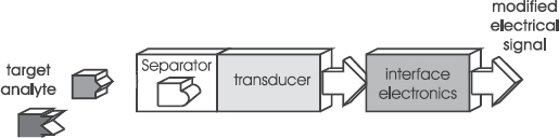
Figure 5.3 Enhancing selectivity by applying pre-separation techniques
5.3 Energy Domains
Physical chemosensors can utilize five different energy domains: optical, thermal, mechanical, magnetic, and electrical. A (nonexhaustive) list of physical properties and effects that are useful for physical chemosensing in the different domains is given in Table 5.1.
Optical principles are often used thanks to the field of analytical chemistry, where optical devices have been applied successfully for a few decades already. The majority of optical sensors in (bio)chemical analysis can be found in absorption and fluorescence measurement, for example, in chromatography or capillary electrophoresis separation setups. Many optical sensors have been realized in silicon technology, the photodiode being the oldest and best known. Other examples are the spectrometer [17], color sensor [18], UV detector [19], and IR sensor [20]. Spectral selectivity can also be obtained by adding optical filters to a detector. A limiting factor for the integration of optical sensing systems is often not the sensor, but the light source, lenses, and filters. Wave-guiding structures and the evanescent-wave fluorescence-excitation of chemicals are subjects of research in several groups [e.g. 21]. Examples that will be described below are commercial pulse-oximetry medical devices, infrared adsorption for oil-degradation monitoring, a biological cell-shape sensor using a diode array, and optical thin film filters in high throughput screening (HTS) devices.
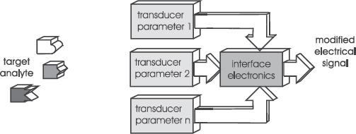
Figure 5.4 Enhancing selectivity by applying multi-physical-parameter sensing
Table 5.1 Examples of physical chemosensors in different energy domains

Thermal effects for physical chemosensing are the thermo-mechanical principle (e.g. the thermal expansion coefficient of liquid mixtures) and heat capacity (amount of energy required to increase the temperature of a gas mixture at a fixed volume or pressure). However, the best-known and most widely used device is the thermal conductivity detector (TCD) for gas and liquid applications. In a portable gas chromatograph, the large heavy stainless steel parts have been replaced by small lightweight components. The thermal conductivity sensor consists of a heated microbeam that is provided with a temperature sensor (e.g. thermistors or thermopiles). If the concentrated gas packages that leave the separation column have a thermal conductance that differs from the carrier gas, the thermal resistivity between the microbeam and the ambient changes results in a temperature change of the microbeam [22]. The first example of an integrated system making use of such a device was the all-silicon gas chromatograph [23]. Many portable gas chromatographs contain such a TCD nowadays.
Another application of the TCD is the measurement of CO2 or He concentration in air, which is possible because the thermal conductivity of CO2 (16.6 × 10⁻³ W/mK) and He (156 × 10−3 W/mK) deviates significantly from air (26.2 × 10⁻³ W/mK).
By monitoring some of the mechanical parameters of a liquid mixture, such as the density, viscosity, and sound velocity, information about the composition is obtained. Surface acoustic wave devices have shown to be very useful for measuring these parameters in liquids. By applying different wave types which have different wave-polarizations, sensitivity to various liquid properties can be ‘designed’. Love-wave devices have been used for viscosity sensing [24] and Lamb-wave devices for viscosity, density, and sound velocity, which gives information about the composition of the liquid [25]. The presence of water in alcohol can be determined with a resolution of 10−4 volume percent [26]. For viscosity sensing, a temperature controlled QCR (quartz crystal resonator) has shown very interesting results [27]. In this study, a heater was integrated into one of the driving electrodes. In this way, measurements at different temperatures can be performed yielding extra information on the fluid.
Another acoustic application is the imaging of intravascular plaques. Atherosclerotic plaques that rupture are a main cause of unstable angina pectoris and acute myocardial infarction. Early diagnosis can be achieved by intravascular acoustic imaging. An acoustic transducer (30 MHz) is placed at the tip of a catheter and, via the groin, is brought to the heart, to make an acoustic image of the plaque on the vascular wall [28].
Micro mass-spectrometers form a generic technique that will be applicable for a wide range of purposes. The drawback is the complexity of the system, which contains so many different parts [29].
Also, the application of the magnetic domain is possible, for example the use of magnetic beads in microchannels as a means to control flow rate or even valves [e.g. 30]. Philips Research has developed a biosensor that measures the magnetic field of magnetic nano-particles that bind to target molecules in a biological assay [31].
Electrical methods include the measurement of conductivity, capacitance, and potential. Renewed interest in conductivity detection in micro capillary electrophoresis (CE) devices has led to different detector configurations [32–34]. An example of a contactless four-electrode conductivity detector for CE devices is given in the next section.
Cell analysis through impedance measurement and impedance spectroscopy is an up-and-coming field (e.g. Coulter counter).
Capacitance measurements are applied to detect changes in dielectric properties, for example, in oil degradation monitoring or in food production.
5.4 Examples and Applications
In this section, several examples and applications of physical chemosensors will be described. The first group of examples concern in situ applications in which the sensors are placed at the measurement location. They include: a blood oximeter connected to the human body, a thermal conductivity gauge for the measurement of gas concentrations, an engine-oil monitoring system using permittivity and viscosity sensors, an infrared sensor system for the determination of oil degradation, and an acoustic oscillator system applied as an electronic nose. The second group of examples are microfluidics devices, in which sample fluids are inserted into a microdevice (chip) for measurement, analysis, or monitoring. The manipulation of these fluids on the chip requires microfluidics design of the channels and sensors, which is described together with the fabrication technology of those devices. The examples given are: contactless conductivity detection in capillary electrophoresis devices, high speed screening arrays, a projection cytometer for detection of microparticles and cells, an on-chip Coulter counter, and dielectrophoresis-based particle sorters.

Figure 5.5 Absorption spectra of haemoglobin (Hb) and oxyhaemoglobin (HbO2)
5.5 Examples of in situ Applications
5.5.1 Blood Oximeter
A device has been developed that solely uses optical means to determine a patient's blood oxygen content: the oximeter. It is now one of the most successful physical chemosensors in the medical field. The absorption spectra of haemoglobin (Hb) and oxyhaemoglobin (HbO2) differ (Figure 5.5), which makes it possible to measure the ratio of both concentrations in blood by measuring the absorption of light of two different wavelengths, e.g. 660 nm and 805 nm. Such a setup can consist of two separate systems, but a color sensor consisting of a single silicon chip can also be used [18, 35]. In pulse oximetry, the heart beat is monitored simultaneously. Several companies offer pulse oximeters, which are attached to a finger or the ear lobe and are applied widely in hospitals to monitor patients.†
5.5.2 Thermal Conductivity Detector
The thermal properties of fluids can be used to analyze these fluids and fluid mixtures. In a thermal conductivity detector (TCD), a hotspot is kept at an elevated temperature by a supply of electrical power. A change in the thermal conductivity of the surrounding fluid – which can be a gas or a liquid – leads to a change in the thermal resistance between the hotspot and the ambient. The temperature of the hotspot changes accordingly. An integrated version of such a device is shown in Figure 5.6 [22]. A cantilever beam was etched free in a silicon substrate. The tip of the cantilever contains a resistive heater. The temperature difference between the tip and the heat sink can be measured by applying a thermopile. If a constant temperature is maintained for the cantilever tip, the power needed to attain this temperature is relative to the heat loss of the tip. Because of the thin cantilever, only a small amount of energy is needed to elevate the temperature. In addition, the thermal resistance of such a thin cantilever is high, which reduces thermal loss. The electrical analogue of the thermal conductivity detector is shown in Figure 5.7.
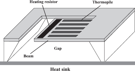
Figure 5.6 Silicon thermal conductivity detector using a thin cantilever beam [22]
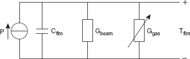
Figure 5.7 Electrical analogue of a thermal conductivity detector [22]
A TCD for leak detection of hydrogen at fuel cells was developed by Bosch [36]. In order to simplify the technology, they did not apply a cantilever or bridge structure but a closed membrane. For the measurement of membrane temperature and ambient temperature, Pt structures were used. The detection limit of this sensor was 0.2% hydrogen in air, which is sufficient for leakage detection in automotive or fuel-cell applications because the lower explosion limit amounts to 4 % hydrogen in the air.
Xensor Integration has developed a universal TCD, which can be applied for several measurement problems.‡ An example of a medical application is the measurement of He concentration in the air, which is used to determine the lung capacity of patients. The measurement is possible because the thermal conductivity of He is six times higher than that of air. Helium traces in the air with values as low as 700 × 10−6 can be measured with these devices. In Table 5.2, the thermal conductivity of different gases is given.
The TCD principle can also be applied for liquids. In [37]. this is applied to determine the deterioration of mineral oils.
Table 5.2 Conductivity of different gases at room temperature
| Gas | κ (300 K) [W/mK] |
| Air | 26.2 × 10⁻³ |
| N2 | 26.1 × 10⁻³ |
| O2 | 26.6 × 10⁻³ |
| CO2 | 16.6 × 10⁻³ |
| H2 | 182 × 10−3 |
| He | 157 × 10−3 |
5.5.3 Engine Oil Monitoring System
The deterioration of engine oil is affected by various parameters such as individual driver operating conditions, environmental conditions, oil quality, and fuel quality. The lifetime of the oil can range from a few thousand to 50 000 km, depending on the load being transported. For reliable determination of the optimum oil change interval, the condition of the oil can be monitored by a sensor system which measures physical oil parameters [38, 39]. It is shown that simultaneously measuring viscosity and permittivity gives insight into different causes of oil deterioration such as fuel dilution, water dilution, soot contamination, or oil oxidation (see Figure 5.8). The viscosity is measured by a microacoustic sensor: a quartz microbalance. The oil permittivity is measured capacitively.
As the oil deteriorates, the measured viscosity increases because of the oxidation of the base oil, build-up of suspended insoluble matter, and dissolved resinous material (combustion residues).
Since the permittivity of engine oil and fuel are similar, fuel dilution will only yield a viscosity change. Soot contamination (diesel engines) influences both viscosity and permittivity. Small amounts of water dilution have a significant influence on the permittivity. Interestingly enough, the microacoustic viscosity sensor is not influenced by the change in viscosity of the bulk fluid due to water dilution. This phenomenon is described in ref. [40].

Figure 5.8 Oil-condition monitoring by viscosity-permittivity measurements
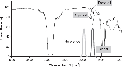
Figure 5.9 FTIR Transmission spectrum of both fresh and artificially aged (8 days) engine oils and the transmittance of the optical filters used by the sensor to compare the absorption values between the oxidation band (1/λ = 1710 cm−1) and the reference band (1/λ = 1970 cm−1)
5.5.4 Oil-condition Sensor Based on Infrared Measurements
Fourier-transform infrared spectroscopy is a well-known method for the analysis of gas and liquid compositions. The IR absorption spectrum depends on the concentration of the molecules present in the sample. For online monitoring, FTIR spectroscopy instrumentation is too expensive and bulky. Therefore, sensor systems focusing on specific wavelengths need to be developed. An example is the monitoring of engine oil deterioration [20]. In this study, the absorption of engine oil at a fixed wavelength was investigated. Oxidation is a measurement for the aging and deterioration of oil; the characteristic adsorption wavelength for oxidized oil is 5.85 μm. In Figure 5.9 it can be seen how the transmission of aged oil decreases at 5.85 μm (1710 cm−1). As a reference, a second measurement was performed at 1970 cm−1 (5 μm), where the oxidation of the oil has no influence on the IR absorption.
5.5.5 Electronic Nose
The topic of the electronic nose and tongue has attracted considerable attention. The mimicking of the human senses still appeals to the imagination. Several systems which use an array of chemical interfaces have shown the ability to distinguish between wines and French cheeses. The reproducibility of these systems has not been proven yet; they need regular calibration. An overview of different principles for electronic noses and a list of commercial suppliers can be found on the website of the Nose-network and Gospel network.1 Metal oxide sensors, conducting polymer sensors, and quartz crystal microbalance sensors with organic active films are mainly used. Mass spectrometry is another method available on the market, but these are still larger systems that need some analysis time. Another system which uses a surface acoustic wave resonator was presented in ref. [16]. A sample is fed to a fast gas chromatograph (GC). As the separated gases leave the GC column, they adsorb (and desorb) at the SAW resonator surface, which results in a resonator frequency shift. Because the device lacks chemical interfaces, it is very fast. The whole process, including separation, takes less than 10 s.
5.6 Microfluidics Devices
Physical chemosensors and biosensors are also applied in on-chip analysis systems. For on-chip analyses of liquids and gases, not only the sensors, but also the channels, heaters, valves, reaction chambers and other elements must be realized on the chip. The fluids are led to a certain location where they are mixed or heated or where they make contact with a specific sensor, etc. Integrated flow-cell systems where small amounts of fluids are manipulated are what we call microfluidics devices.
In sheath-flow microfluidics devices, multiple flows are combined within a single channel. The sample flow contains the liquid of interest that needs to be analyzed. The second liquid (the sheath liquid) is the carrier liquid, which has the function of focusing the sample liquid and controlling the location of the sample liquid with respect to the sensor interface. A flow-cell which generates a sample flow and allows adjustments of the effective aperture in two dimensions is shown in Figure 5.10 [41]. In this device, the sheath flow setup consists not only of a sample flow (that enters the chip through a hole in the silicon plate) and a transparent carrier flow (which, in Figure 5.10, enters the chip from the left), but also of two additional side ports through which carrier liquid can be added or removed from the main channel. In Figure 5.11, the three-dimensional setup of the flow cell is depicted.
If liquid is added through the side ports, the width of the sample flow will be decreased; if liquid is removed, the width of the sample flow increases, as can be seen in the simulation in Figure 5.12. The height of the sample flow depends on the ratio of the injected sample flow and the carrier flow rates. Increasing the relative sample flow-rate results in a higher ‘penetration’ of the sample flow into the channel. In this flow system, the height and width of the sample flow can be controlled. Since the sample flow remains in contact with the bottom of the channel, we call this a noncoaxial sheath-flow setup.
One of the applications of such noncoaxial fluidic devices is the analysis of particles and cells. In order to verify whether particles stay within the sample flow during their journey through the analysis part of the device, a test was performed where the sample flow was switched to a side channel. The polystyrene particles (diameter 20 μm) stay within the sample flow and do not enter the carrier flow, which confirmed the usefulness of this noncoaxial sheath fluidics for particle analysis.
For the fabrication of microfluidics devices, different materials are available. Silicon technologies for sensor fabrication have become developed. Whether or not to use a silicon micro- (or nano-) system and whether or not to combine electronic circuitry and sensor devices either in a single chip or in a single package has been an interesting topic of discussion for a long time now [42]. The fact is that miniaturization of chemosensors and biosensors yields not only the known benefits of microsystems in general (small, reliable, potential low-cost, IC-compatible) but also some field-specific ones such as high-throughput handling, simultaneous testing, and (quasi) real-time monitoring.
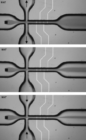
Figure 5.10 Photographs of noncoaxial sample flows in a sheath-flow device using side ports for adding or removing carrier liquid from the main channel. The effect on the width of the sample flow is clearly visible. The channel width at the location of the electrodes amounts to 160 μm

Figure 5.11 Noncoaxial sheath flow cell: this flow cell creates a noncoaxial sheath flow and allows controlling of the sample flow dimensions; here the control ports are used to widen the sample flow

Figure 5.12 Sample-flow width and height are controlled dynamically by adding or removing sheath liquid through the side ports
Wafer-to-wafer bonding technologies have become highly significant because of the need for microchannels in which the analytes and carriers can be transported and manipulated. The channels etched in one wafer are capped by a second wafer using anodic bonding (e.g. glass-to-silicon) or direct bonding (e.g. silicon-to-silicon, see photo in Figure 5.13). The anodic bonding is a less complex process yielding higher bond strengths and greater reliability.
A glass-to-glass anodic bonding process (see Figure 5.14) [43, 44] is expected to find its way into many fluidic devices because of its simplicity, relatively low bonding temperature (350 to 400) °C, high bond strength (20 MPa), and because of the possibility to integrate metal microelectrodes. A thin film of silicon or silicon nitride is deposited on one of the glass wafers after which anodic bonding of two glass wafers is possible.

Figure 5.13 Silicon-to-silicon bonded structure by direct bonding at a low temperature (120°C). The channel is 7 μm wide and 600 nm high

Figure 5.14 Glass-to-glass bonded wafers using anodic bonding. The wafers are each 0.5mm thick. The channel is 60 μm wide and 20 μm high
A wafer-bonding technology that has appeared in the recent past is SU-8 resist bonding. SU-8 is an epoxy available with different viscosities, which allows resist thicknesses of more than 500 μm [45]. Therefore, fluid channels can be directly defined in this layer, which means that channel etching in glass or silicon can be omitted. A wafer-bonding process with a high yield and reliable bonding over the whole wafer surface is described in [46]. In Figure 5.15, a cross-view of an SU-8 bonding structure is shown, where two channels are built on top of each other, separated by a silver film.
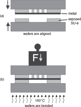
Figure 5.15 SU-8 double-channel construction using an intermediate silver layer. After the patterning of SU-8 on both wafers and the deposition of a silver layer on the top wafer, alignment and bonding are performed
Another important development for fluidic devices is the use of plastics [e.g. 13]. The advantages of plastics are the simple fabrication and the low production costs of such devices. A disadvantage is that the technology does not allow easy integration of functionality on the plastic chip (such as microelectrodes).
Information on other parts of microsystems, such as pumps, channels, valves, reaction chambers, mixers, splitters, and electrophoresis channels, can also be found in other conference proceedings [47] and a vast amount of publications in several journals.
In the following sections, examples of microfluidics devices for physical chemosensing will be described.
5.6.1 Projection Cytometer
Cytometers are instruments used for particle analysis that are based on the optical properties of the particle. Different integrated sheath-flow chambers have been presented in the literature (the early ones in [48, 49]), but the optical sensor is often not located on the chip. By integrating the optical sensor, the measurement system becomes much smaller. On-chip optical analysis methods have been developed for measuring not only the size of microparticles but also the shape and optical properties. The integrated cytometer that is based on optical projection consists of an optically transparent flow channel with a light-source positioned above it. On the bottom of the flow channel, a one-dimensional strip-photodiode is placed perpendicular to the direction of the flow. When a particle passes the photodiodes, it partially blocks the light. A cross-section of the shadow is registered by the photodiodes. The channel width and height are typically 100 μm. A sheath flow assures that the particles flow close to the sensor (Figure 5.16) [50]. The optical sensors used consist of strip-shaped photodiodes. They have a junction of 50 μm wide and 2 μm long (Figure 5.17). They detect the projection of a passing particle, which allows a two-dimensional measurement of the particle shape. In the case of semitransparent particles, optical properties can be determined at the same time.

Figure 5.16 Schematic diagram of the particle shape sensor
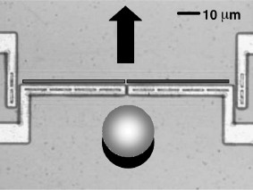
Figure 5.17 The particle shadow (projection) is detected by the two strip-photodiodes
A lock-in amplifier was used to modulate (25 kHz) a laser source (532 nm wavelength) and to demodulate the signal being generated by the integrated photodiode. When a particle (or cell) passes the photosensitive area of the sensor, its optical properties are expected to change the signal. A digital storage oscilloscope was used to record the pulses that were generated in this way.
Figure 5.18 gives the photodiode response to transparent and nontransparent polystyrene particles that flow through the channel. Interestingly, the transparent particles show an increase of photocurrent instead of a drop. This is due to the lens effect, as illustrated in Figure 5.19. The light is refracted inwards at the particle and when they leave the particle, the light rays are again refracted. It makes the optical system very promising for the detection and analysis of particles with different optical properties, such as cells. In Figure 5.20, a measurement series of yeast cells and of Chinese hamster ovary (CHO) cells are shown [51]. Because of the transparency of the cells, the photocurrent yields a positive peak. The reproducibility of this measurement series appears to be less high in comparison to the polystyrene beads. This is due to a larger size distribution of the cells and to the fact that cell surfaces are less smooth than polystyrene particles. The CHO cells have a larger diameter (about 15 μm) than the yeast cells (about 4 μm), therefore the peak response of CHO cells is higher. The measurement shows that different cells give a different optical response, which allows cell recognition.
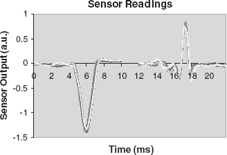
Figure 5.18 The ten measurements printed on top of each other for 20 μm diameter silver-coated particles (left) and 24 μm diameter plain particles (right) demonstrate good repeatability

Figure 5.19 The different pulse shapes obtained with the silver-coated particle (left) and the plain, transparent particle (right) can be explained by their optical properties
Photos of the optical chips are shown in Figure 5.21. The chip on the left contains a fluidic channel that was etched in the glass plate. Because of the isotropic etching process, the cross-section of the channel has a curved shape, which affects the optical performance. The chip on the right was made by SU-8 wafer bonding of the silicon and glass wafer. The channels were defined in the SU-8 resist film resulting in a rectangular channel shape, which yields better optical properties.
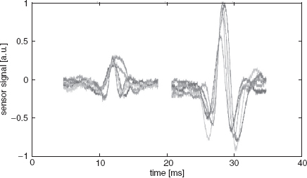
Figure 5.20 Measurement series of yeast cells (left, diameter circa 4 μm) and CHO cells (right, diameter circa 15 μm). Since they are transparent, the cells yield a positive peak
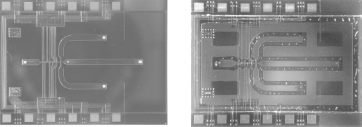
Figure 5.21 Cytometer chip (1.5 cm × 2 cm). Silicon-to-glass bonded structures (anodic bonding in the left chip, SU-8 bonding in the chip on the right)
5.6.2 Coulter Counter
The Coulter counter is an instrument used for measuring particle-size distribution in medical and industrial applications. W.H. Coulters patent was granted in 1953 [52]. A conductive liquid in which the particles have been suspended is pumped through a small aperture. The electrical resistance over the aperture is monitored and, when a particle passes the aperture, an increase is measured in the resistance that is proportional to the volume of the particle. For an ideal homogeneous electrical field and a spherical particle, the change in resistance becomes [53] :

where ρl is the impedance of the sample liquid, rp is the radius of the particle, and Ach is the cross-sectional area of the aperture (channel). The formula shows that the ratio between particle size and the area of the aperture determines the sensitivity of the instrument. In the derivation of this formula it was assumed that the length of the Coulter aperture equals the diameter of the particle. In practice, the aperture length is typically larger, which reduces the observed change in impedance. In Figure 5.22, a schematic overview of the Coulter counter is shown.
The integrated Coulter counter contains a flow-cell to generate a sheath flow that allows an adjustment of the effective aperture in two dimensions by tuning the flow rate of a conductive sample flow and a nonconductive sheath flow (see Figure 5.23).
This approach has two advantages. Firstly, the compromise of the size of the Coulter aperture is circumvented, since the chance of clogging depends on the physical dimension of the channel, while the sensitivity is determined by the dimensions of the sample-liquid flow (effective aperture), which can be much smaller (to as little as a few percent of the channel width). This means that a high sensitivity can be achieved while keeping the chance of clogging low (see Figure 5.24). The second advantage is that the dimensions of the aperture can be adapted to the size of different samples. The horizontal and vertical dimensions of the Coulter aperture are controlled by the external flow rates of the sample liquid and sheath flow. These control mechanisms allow the dimensions of the effective Coulter aperture to be adapted without the need to exchange any parts. Figure 5.25 shows the potential of the method: in a measurement series using 20 and 24 μm diameter particles, the measurements match the specification of the particles (Plain polystyrene microspheres, with a diameter of 24 μm ± 2 %, Polymer Laboratories, and silver-coated polystyrene microspheres, with a diameter of 20 μm ± 0.5 %, Microparticles GmbH.) The sample flow was a 5 % NaCl solution (7.8 S/m); the carrier liquid was deionized water [54].

Figure 5.22 Schematic overview of the Coulter counter from the original patent US 2,656,508 (1953) http://www.uspto.gov

Figure 5.23 Conductive sample liquid (dark) surrounded by nonconductive carrier liquid (transparent). In the smaller part of the channel the four Coulter counter electrodes have been realized
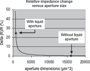
Figure 5.24 Theoretical relation between aperture dimensions and the relative change in impedance for a 25 μm spherical particle in a 160 μm × 100 μm channel and in a 40 μm diameter sample flow
5.6.3 Dielectrophoresis-based Devices
Dielectrophoresis is the effect that a polarizable particle experiences a force when it is exposed to a nonuniform electric field [55]. For the description of the particle behavior in a fluidic channel, dielectrophoretic and hydrodynamic forces are taken into account. By using a dipole approximation for a polarized particle in an electric field and utilizing the so-called Stokes approximation for the hydrodynamic drag, the forces acting on a particle read:
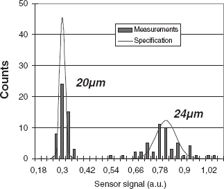
Figure 5.25 Histogram of 50 measurements with particles of 20 μm diameter (left) and 24 μm (right); the solid line represents the supplier's specification of the particles
where K = (εp − εl)/(εp + 2εl) is the so-called Clausius–Mossotti factor and εl and εp are the permittivities of the liquid and of the particles, respectively. R is the particle radius, E0 is the local electric field, η is the viscosity of the liquid, and νl − νp is the difference of liquid and particle velocity. The equilibrium between these expressions and the buoyancy force are used in a model to determine the trajectory of a particle in a channel of given electric and flow field distribution.
DEP separator
One method to separate different particles in the flow is to apply dielectrophoretic (DEP) forces by introducing a set of periodical electrodes at the top and bottom of the flow channel. Polystyrene particles in a watery environment experience a repelling force (negative DEP) from the electrodes of the periodic array, which causes the particles to move up and down as they are moved through the channel by hydrodynamic drag forces [56]. Since the DEP effect strongly depends on the diameter of the particles, the amplitude of the vertical displacement is a function of the particle diameter as well. Because of the parabolic velocity profile of the pressure-driven flow, larger particles (for which the amplitude of the vertical displacement is larger) have a lower average transit velocity. This results in longer retention times for larger particles (see Figure 5.26). This device does not use gravity as a parameter for separation.
For characterization of the device, deionized water containing polystyrene test particles was continuously pumped through the device using syringe pumps. A DEP trap structure inside the chip periodically released particles into the channel and the retention time was measured by using a stopwatch. With two different frequency generators, the trap structure and the separation electrodes were supplied at 1 MHz and voltages between 5 V (for separation) and 12 V (for trapping) RMS. Figure 5.26 depicts the separation of differently sized particles using the in-channel DEP array. A photo of the 15 × 20 mm2 chip is shown in Figure 5.27. A measurement series of the separation of 8 μm and 15 μm diameter polystyrene particles is shown in Figure 5.28. The difference in retention time is about 2 s (8.5 s for the smaller particles, 10.5 s for the larger particles.)
DEP sorter
Several integrated particle sorters that are based on different actuation principles have been presented in the literature. Thermal actuators can be used to locally heat a channel and cause an increase (based on a sol–gel process [57]. or decrease [58] in viscosity of the liquid in one of the branches of a channel junction; this controls the flow distribution between the two branches. Magnetic actuation has been applied for the sorting of particles, where a strong magnetic field pulls the magnetic [59] or magnetically labeled [60] particles into the desired output channel. Sorters based on mechanic actuation apply either internal [61] or external valves [e.g. 62] to switch the flow to the desired channel branch. Electric actuation has also been extensively used to sort particles [e.g. 63]. A more recent development are optical tweezers [64].
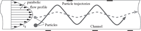
Figure 5.26 Drawing of the DEP separator flow channel with DEP electrodes on the top and bottom of the channel
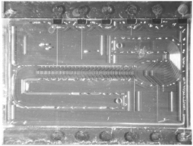
Figure 5.27 The DEP separator chip: glass-glass structure bonded by an SU-8 layer
The sorting of microparticles can also be obtained by applying dielectrophoresis. It is attractive for application in microfluidics devices because it requires no moving parts, labeling, or high voltages. The actuators consist of simple electrodes that are fabricated in the flow channel. These electrodes can generate strong field gradients, which is enough to move particles that flow-by in the channel. Different types of DEP particle sorting can be distinguished. The two-dimensional spatial separation of binary mixtures of particles has been demonstrated for several types of particles [e.g. 65–67], even for particles in the sub-micron range. A sorter based on the temporary trapping of particles is presented in [68] and several flow-through DEP sorters have been published [e.g. 69, 70].

Figure 5.28 Retention time measurements of 8 and 15 μm diameter polystyrene particles
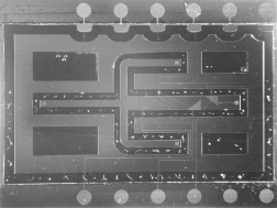
Figure 5.29 Photograph of the sorter chip (15 mm × 20 mm)
Flow-through particle sorters are shown in Figure 5.29 and in Figure 5.30. This sorter makes use of triangle-shaped electrodes located on the top and bottom of the channel through which the particles flow. At the edges of the electrodes, the electrical field between these electrodes is nonuniform and, in the case of negative dielectrophoresis, repels the particles, which results in a movement of the particles sideways. By placing such focusing electrode structures in series, the sorting of particles to a certain branch can be accomplished [71]. On the left side of Figure 5.30 three outlet branches are visible. The design aspects of such devices are electrode geometry (line electrodes, triangle electrodes), location of the electrodes (top and bottom versus bottom only), Joule heating that might occur in the liquid due to the applied voltages at the electrodes, and maximum flow speed. With the sorter shown, polystyrene particles (24 μm diameter) were sorted by a switching voltage on the electrodes of a few volts up to 9V (ac, 1MHz). The maximum flow speed was 8 mm/s in a channel 1mm wide and 70 μm high.
Figure 5.30 Detailed photo of the electrodes of a DEP sorter chip. The channel is 1mm wide and 70 μm high. The sorted polystyrene particles have a diameter of about 20 μm

Figure 5.31 Silicon high-throughput screening device 1 cm × 2 cm
5.6.4 High-throughput Screening Arrays
A fascinating development is the application of combinatorial chemistry, which uses small reactor arrays made in chips called high-throughput screening (HTS) arrays. They allow a large number of tests to be conducted in a very short time. The sample volumes can be as small as 1nl, a factor 106 smaller compared to the widely used 8 × 12 titer plates in which the individual reaction chambers have a volume of about 1ml. The chip permits functional integration in every reactor. In addition to drug screening and DNA research, those HSS devices can be applied in enzymatic analysis and clinical chemistry. A silicon device containing a 5 × 5 array is shown in Figure 5.31. The typical size of a well implemented in silicon is 200 μm × 200 μm × 25 μm, which represents a volume of only 1nl. To read out the optical activity in the wells (fluorescence), a CCD camera is usually placed above the array chip [72]. On the chip, instead of a camera, integrated optical sensors can be integrated in each well. A photodiode provided with a thin-film optical filter of crystalline silicon (Figure 5.32) shows a very high visible-over-UV selectivity [73] (Figure 5.33), which allows analysis of the enzymatic activity by means of NADH (nicotinamide adenine dinucleotide) detection:
![]()

Figure 5.32 Cross-view of a nanoliter well provided with an integrated photodiode and a crystalline silicon film as UV filter

Figure 5.33 Transmittance of a polysilicon film grown on glass compared to simulations
Many dehydrogenase enzymes can use the coenzyme NADH to transfer hydrogen groups between molecules. NADH emits at 450 nm when it is excited with UV (340 nm). The UV radiation is absorbed in the crystalline silicon film, where the visible light at 450nm is transmitted and detected by the integrated photodiode. A measurement of NADH concentration through fluorescence detection is shown in Figure 5.34.
5.6.5 Contactless Conductivity Detection in CE
In capillary electrophoresis systems, a sample is brought into a channel, and by applying a high electric voltage over the liquid in the channel, an electroendoosmotic flow is initiated. At the same time, separation of the ions takes place. As a result, each ion has its typical retention time, which depends on its mobility. For detection laser-induced fluorescence (LIF) is often used.
Measurement of the liquid electrical conductivity seems obvious because the separation method applied is based on the electrical behavior of the sample components. For many years, conductivity detection appeared problematic and inaccurate compared to fluorescent detection. Renewed interest in conductivity detection (labeling can be omitted and the conductivity detector can be made much smaller than the current optical measurement systems) has led to the design of a new integrated contactless four-electrode detector with interesting features [74]. The detector has a linear response for a large frequency range and a detection limit of about 20 μM. In Figure 5.35, a photo of a glass-implemented CE device containing an integrated conductivity detector is shown. In Figure 5.36, a measurement series is depicted showing the separation and detection of six different acids (1mM each), obtained with the device in Figure 5.35.
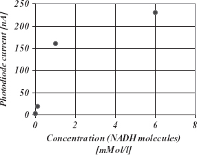
Figure 5.34 Photodiode current vs NADH concentration

Figure 5.35 Contactless conductivity detector (insert) in a glass CE device
5.7 Conclusions
In general, it can be stated that the development of physical chemosensors is less complex than the development of direct chemical sensors. This is attributed to the fact that the manufacturing of a chemical interface can be omitted and that a chemical reaction at the transducer is not required. The sacrifice could be a lower selectivity and a lesser detection limit. However, in many of the measurement problems in the chemical or biochemical field, a very low detection limit is not needed. Sample pre-separation or multiparameter sensing are practical methods to improve selectivity. If physical measurements can yield the required information, the development of a physical chemosensor or a physical biosensor should be considered.

Figure 5.36 Separation of (1) fumaric, (2) citric, (3) succinic, (4) pyruvic, (5) acetic, and (6) lactic acid (1mM each). Applied separation field 250 V/cm
For many chemical and biochemical sensors, microfluidics cells have become a necessity. These cells can be on-chip integrated and can allow the manipulation and control of the different fluids and flows. The development of different technologies for microfluidics devices such as glass, silicon, plastics, and SU-8, is still ongoing. The costs and integration of functionality are the main considerations in deciding which technology to use for a certain application.
The further development of physical-chemosensor systems and their appliance in new fields will be the challenge for the years to come.
Problems
5.1 In Section 5.6 the use of a noncoaxial sheath flow device was discussed. How would you extend the design of this microfluidics device in order to obtain a sample flow which is coaxially surrounded by carrier flow?
5.2 (a) In an integrated Coulter counter an adaptive noncoaxial sample flow is used to adjust the sensitivity to the particle size that is being measured. The sample flow diameter is set to 50 μm diameter. Calculate, using Equation (5.1), the change in resistance caused by spherical particles that are present in the sample flow, for particles of 5 μm to 40 μm diameter in steps of 1 μm. Plot the results in a figure showing the change in resistance versus the particle diameter. What can you say about the sensitivity of the system for the different particle diameters?
(b) What is the dimension of the resistivity of the liquid in Equation (5.1)?
References
[1] Taylor, R.F. and Schultz, J.S. (eds) (1996). Handbook of Chemical and Biological Sensors, IOP, Bristol, p. 1.
[2] Goepel, W., Hesse, J. and Zemel, J.N. (eds) (1991). Sensors, a Comprehensive Survey, Chemical and Biochemical Sensors, Part I, VCH, p. 2.
[3] Expanding the Vision of Sensor Materials (1995). National Academy Press, Washington, DC.
[4] Moseley, P.T. and Tofield, B.C. (eds) (1987). Solid State Gas Sensors, Adam Hilger, Bristol, p. 234.
[5] Lambrechts, M. and Sansen, W. (eds) (1992). Biosensors: Microelectrochemical Devices, IOP, Bristol, p. 280.
[6] Taylor, R.F. and Schultz, J.S. (eds) (1996). Handbook of Chemical and Biological Sensors, IOP, Bristol, pp. 555–563 and pp. 573–577.
[7] Spichiger-Keller, U.E. (1998). Chemical Sensors and Biosensors for Medical and Biological Applications, Wiley-VCH, New York, pp. 6–13.
[8] Diamond, D. (ed.) (1998). Principles of Chemical and Biological Sensors, Wiley, New York, p. 8.
[9] Ramsay, G. (ed.) (1998). Commercial Biosensors, Wiley, New York, p. 41.
[10] Sonnleitner, B. (ed.) (1999). Advances in Biochemical Engineering Biotechnology, Springer, Berlin, p. 54.
[11] Graber, N., Luedi, H. and Widmer, H.M. (1990). The use of chemical sensors in industry. In S&A B1, pp. 239–243.
[12] Manz, A. Graber, N. and Widmer, H.M. (1990). Miniaturized total chemical analysis systems: a novel concept for chemical sensing. In S&A B1, pp. 244–248.
[13] Micro total analysis systems (2005). In Proc. μTAS 2005 Symp. Boston, USA, eds. Jensen, K.F., Han, J., Harrison, D.J. and Voldman, J., TRF.
[14] Vellekoop, M.J. (2001). The emergence of physical chemosensors and biosensors. In Proc. Transducers 01, Munich, Germany.
[15] Jakoby, B. (2000). Microacoustic sensors for automotive applications. In Proc. 2000 IEEE Ultrasonics Symp., San Juan, Puerto Rico.
[16] Staples, E.J. (1999). The zNosetm, a new electronic nose using acoustic technology. In Proc. 1999 IEEE Ultrasonics Symp., Lake Tahoe, USA, pp. 417–423.
[17] Kwa, T.A. (1995). Integrated silicon spectrometer, Ph.D. Thesis, Delft University Press.
[18] Wolffenbuttel, R.F. and de Graaf, G. (1990). Performance of an integrated silicon colour sensor with a digital output in terms of response to colours in the colour triangle. In S&A A21–23, pp. 574–580.
[19] Popovic, R.S., Solt, K. Falk, U. and Stoessel, Z. (1990). A silicon ultraviolet detector. In S&A A21-A23, pp. 553–558.
[20] Agoston, A., Ötsch, C., Zhuravleva, J. and Jakoby, B. (2004). An IR-absorption sensor system for the determination of engine oil deterioration. In Proc. IEEE Sensors Conference 2004, Vienna, pp. 463–466.
[21] Simpson, T.R.E., Revell, D.J., Cook, M.J. and Russell, D.A. (1997). Evanescent wave excited fluorescence from self-assembled phthalocyanine monolayers, Langmuir, 13, 460–464.
[22] Meijer, G.C.M. and van Herwaarden, A.W. (1994). Thermal Sensors, IOP, Bristol.
[23] Terry, S.C., Jerman, J.H. and Angell, J.B. (1979). A gas chromatograph air analyzer fabricated on a silicon wafer, IEEE Transactions on Electron Devices, ED-26, 1880.
[24] Jakoby, B. and Vellekoop, M.J. (1998). Viscosity sensing using a Love-wave device. In S&A A 68, pp. 275–281.
[25] Ballantine, D.S., White, R.M., Martin, S.J., Ricco, A.J., Zellers, E.T., Frye, G.C. and Wohltjen, H. (1997). Acoustic Wave Sensors, Theory, Design, and Physico-chemical Applications, Academic Press, New York.
[26] Vellekoop, M.J., Lubking, G.W. Sarro, P.M. and Venema, A. (1994). Integrated-circuit-compatible design and technology of acoustic-wave based microsensors. In S&A A44, pp. 249–263.
[27] Jakoby, B., Klinger, F.P. and Svasek, P. (2005). A novel microacoustic viscosity sensor providing integrated sample temperature control, Sensors and Actuators A: Physical, 274–280.
[28] de Korte, C.L., Pasterkamp, G., van der Steen, A.F.W. and Woutman, H.A. (1999). Characterisation of plaque components with IVUS elastography. In Proc. 1999 IEEE Ultrasonics Symposium, Lake Tahoe, USA, pp. 1645–1648.
[29] Henry, C.M. (1999). The incredible shrinking mass spectrometers, Analytical Chemistry News & Features, April 1, pp. 264A–268A.
[30] Zeuner, A., Richter, R. and Rehberg, I. (1998). Experiments on negative and positive magnetoviscosity in an alternating magnetic field, Physical Review E, 58, 6287–6293.
[31] Janssen, X.J.A., van IJzendoorn, L.J. and Prins, M.W.J. (2008). On-chip manipulation and detection of magnetic particles for functional biosensors, Biosensors and Bioelectronics 23, 833.
[32] Laugere, F., Lubking, G.W., Berthold, A., Bastemeijer, J. and Vellekoop, M.J. (1999). A novel high-resolution liquid-conductivity detector. In Proc Eurosensors XIII, The Hague, The Netherlands, pp. 211–214.
[33] Weber, G., Joenck, M., Siepe, D., Neyer, A. and Hergenroeder, R. (2000). CE with direct and contactless conductivity detection on a polymer microchip. In Proc. μTAS 2000 Symp., The Netherlands, eds. van den Berg, A., Olthuis, W. and Bergveld, P., Kluwer, Dordrecht, pp. 383–386.
[34] Solinova, V. and Kasicka, V. (2006). Recent applications of conductivity detection in capillary and chip electrophoresis, Review, Journal of Separation Science, 29, 1743–1762.
[35] Goosen, J.F.L., French, P.J. and Sarro, P.M. (2000). Pressure, flow and oxygen saturation sensors on one chip for use in catheters. In Proc. IEEE 13th Annual International Conference on MEMS, Japan, pp. 537–540.
[36] Simon, I. and Arndt, M. (2002). Thermal and gas-sensing properties of a micromachined thermal conductivity sensor for the detection of hydrogen in automotive applications, Sensors and Actuators A, 97–98, 104–108.
[37] Kuntner, J., Chabicovsky, R. and Jakoby, B. (2005). Sensing the thermal conductivity of deteriorated mineral oils using a hot-film microsensor, Sensors and Actuators A, 123–124, 397–402.
[38] Bertrand, P., Scherer, M., Hilberath, T. and Jakoby, B. (2004). Oil condition monitoring sensor for diesel engines. In Proceedings of the International Congress The Diesel Engine: Today and Tomorrow, May 2004 R- 2004–05–04.
[39] Jakoby, B. and Hermann, F. (2003). Chemical sensors for liquid media. In Sensors Applications, Vol. 4: Sensors for Automotive Applications, eds. Marek, J., Trah, H.-P., Suzuki, Y. and Yokomori, I., Wiley-VCH, New York, pp. 516–527.
[40] Jakoby, B. and Vellekoop, M.J. (2004). Physical sensors for water-in-oil emulsions, Sensors and Actuators A, 110, 28–32.
[41] Nieuwenhuis, J.H., Bastemeijer, J., Sarro, P.M. and Vellekoop, M.J. (2003). Integrated flow-cells for novel adjustable sheath flows, Lab Chip, 3, 56–61.
[42] Wolffenbuttel, R.F. (ed.) (1996). Silicon Sensors and Circuits: On-chip Compatibility, Chapman & Hall, London.
[43] Strato, H.R.C. (1994). Glass technology, recess etching, electrode fabrication and anodic bonding, Thesis report, TU Delft, Electronic Instrumentation Lab, A94–09.
[44] Berthold, A., Nicola, L., Sarro, P. and Vellekoop, M. (2000). Glass-to-glass anodic bonding with standard IC technology thin films as intermediate layers, Sensors and Actuators, A82, 224–228.
[45] Nguyen, N.-T. and Wereley, S.T. (2002). Fundamentals and Applications of Microfluidics, Artech House, Boston, MA, pp. 99–103.
[46] Svasek, P., Svasek, E., Lendl, B. and Vellekoop, M.J. (2004). Fabrication of miniaturized fluidic devices using SU-8 based lithography and low temperature wafer bonding, Sensors and Actuators A, 115, 591–599.
[47] Proc. μTAS workshops, Proc. IEEE Sensors Conferences, Proc. Transducers Conferences, Proc. Eurosensors Conferences.
[48] Miyake, R., Ohki, H., Yamazaki, I. and Yabe, R. (1991). A development of micro sheath flow chamber. In Proc. MEMS ‘91, pp. 265–270.
[49] Sobek, D., Young, A.M., Gray, M.L. and Senturia, S.D. (1993). A microfabricated flow chamber for optical measurements in fluids. In Proc. MEMS ‘93, pp. 219–224.
[50] Nieuwenhuis, J.H., Bastemeijer, J., Bossche, A. and Vellekoop, M.J. (2003). Near-field optical particle-shape sensors for application in an integrated cytometer, IEEE Sensors Journal, 3, 646–651.
[51] Kostner, S. and Vellekoop, M.J. (2006). Optical detection of different biological cells in an integrated projection cytometer. In Proc. IEEE Sensors Conference, Daegu, South Korea.
[52] Coulter, W.H. (1953). Means for counting particles suspended in fluids, US Patent 2,656,508.
[53] Koch, M., Evans, A. and Brunnschweiler, A. (2000). Microfluidic Technology and Applications, 1st edn, Baldock: Research Studies Press.
[54] Nieuwenhuis, J.H. (2005). Microsystems for particle analysis, PhD thesis, ISBN 3–85465–014–0.
[55] Jones, T.B. (1995). Electromechanics of Particles, Cambridge University Press, Cambridge.
[56] Kostner, S., Nieuwenhuis, J.H., Svasek, E., Svasek, P., Jachimowicz, A. and Vellekoop, M.J. (2004. Continuous particle separator based on periodical DEP elements. In Proc. microTAS 2004, Malmö, Sweden, pp. 9–11.
[57] Tashiro, K., Ikeda, S., Sekiguchi, T., Shoji, S., Makazu, H., Funatsu, T. and Tsukita, S. (2001). A particles and biomolecules sorting micro flow system using thermal gelation of methyl cellulose solution. Presented at MicroTAS, Monterey, CA.
[58] Schulz, T., Poser, S., Ermantraut, E., McCaskill, J., Mathis, H. and Köhler, J.M. (1998). Miniaturized electrocaloric flow controller for analyte multiplexing and cell/particle sorting. Presented at MicroTAS, Banff, Alberta, Canada.
[59] Chronis, N., Lam, W. and Lee, L. (2001). A microfabricated bio-magnetic separator based on continuous hydrodynamic parallel flow. Presented at MicroTAS, Monterey, CA.
[60] Telleman, P., Larsen, U.D., Philip, J., Blankenstein, G. and Wolff, A. (1998). Cell sorting in microfluidic systems. Presented at MicroTAS, Banff, Alberta, Canada.
[61] Fu, A., Spence, C., Scherer, A., Arnold, F. and Quake, S. (1999). A microfabricated fluorescence-activated cell sorter, Nature Biotechnology, 17, 1109–1111.
[62] Blankenstein, G. and Larsen, U.D. (1998). Modular concept of a laboratory on a chip for chemical and biochemical analysis, Biosensors & Bioelectronics, 13, 427–438.
[63] Schnelle, T., Müller, T., Gradl, G., Shirley, S.G. and Fuhr, G. (1999). Paired microelectrode system: dielectrophoretic particle sorting and force calibration, Journal of Electrostatics, 47, 121–132.
[64] Hirano, K. and Baba, Y. (2002). Optical recovery of particles on a chip toward cell sorting and bead-bed detection. Presented at MicroTAS, Nara, Japan.
[65] Morgan, H., Hughes, M.P. and Green, N.G. (1999). Separation of submicron bioparticles by dielectrophoresis, Biophysical Journal, 77, 516–525.
[66] Cui, L., Holmes, D. and Morgan, H. (2001). The dielectrophoretic levitation and separation of latex beads in microchips, Electrophoresis, 22, 3893–3901.
[67] Li, H. and Bashir, R. (2002). Dielectrophoretic separation and manipulation of live and heat-treated cells of Listeria on microfabricated devices with interdigitated electrodes, Sensors and Actuators B, 86, 215–221.
[68] Voldman, J., Gray, M.L., Toner, M. and Schmidt, M.A. (2002). A microfabrication-based dynamic array cytometer, Analytical Chemistry, 74, 3984–3990.
[69] Fiedler, S., Shirley, S., Schnelle, T. and Fuhr, G. (1998). Dielectrophoretic sorting of particles and cells in a microsystem, Analytical Chemistry, 70, 1909–1915.
[70] Holmes, D., Green, N.G. and Morgan, H. (2003). Microdevices for dielectrophoretic flow-through cell separation, IEEE Engineering in Medicine and Biology Magazine, 22, 85–90.
[71] Nieuwenhuis, J.H. and Vellekoop, M.J. (2005). Optimisation of microfluidic particle sorters based on dielectrophoresis, IEEE Sensors Journal, 5, 810–816.
[72] van Den Doel, L., Vellekoop, M., Sarro, P., Picioreanu, S., Moerman, R., Frank, H., van Dedem, G., Hjelt, K., Young, I. (1998). Fluorescence detection in (sub)-nano liter microarrays. In Proc. ASCI ‘98, Lommel, Belgium, pp. 58–62.
[73] Iordanov, V.P., Lubking, G.W., Ishihara, R., Wolffenbuttel, R.F., Sarro, P.M. and Vellekoop, M.J. (2001). Si based thin-film filter with high visible-over-UV selectivity for biochemical fluorescence analysis. In Proc. Transducers ‘01, Munich, Germany.
[74] Laugere, F., Berthold, A., Lubking, G.W., Bastemeijer, J., Guijt, R.M., Baltussen, E., Sarro, P.M. and Vellekoop, M.J. (2001). Experimental verification of an improved method for conductivity detection in on-chip capillary electrophoresis systems. In Proc. Transducers ‘01, Munich, Germany.
* e.g. Affymetrix (www.affymetrix.com), Agilent (www.agilent.com), Caliper (caliperls.com), Cepheid (cepheid.com), C2V (microproducts.nl), Micralyne (micralyne.com), Nanogen (nanogen.com), Xensor Integration (xensor.nl), Lionix (Lionixbv.nl).
† e.g. www.oximeter.org.
1 http://www.nose-network.org/, http://www.gospel-network.org/
Smart Sensor Systems Edited by Gerard C.M. Meijer
© 2008 John Wiley & Sons, Ltd