
Solutions to Problems
Chapter 2
Solution to Problem 2.1
(a) What is the shape and magnitude of the amplifier output voltage V0?
Figure 1(a) shows an equivalent circuit diagram of the front-end amplifier, including the cable capacitances, where Cp1 = Cp2 = 100 pF. Capacitor Cp1 charges the excitation voltage source. However, because of the low impedance (zero ohm), this has no effect on the voltage across the sensor capacitor Cs. With respect to Cp2 it can be noted that, with an ideal amplifier, the amplifier input voltage equals 0 V. Because this voltage equals the voltage over Cp2, the current through Cp2 equals zero. Therefore, the current Ii (Figure 1(a)) equals
where s represents the Laplace operator. The output voltage V0 equals
Equation (2) shows that the amplifier with its feedback circuitry has a real amplification factor, which equals Cs/Cf = 1/5. Therefore, the output voltage is a square-wave voltage with a peak-to-peak value of 2 V.
(b) What is the shape and magnitude of the amplifier output voltage V0 for this modified circuit configuration?
Figure 1(b) shows the equivalent circuit diagram of the front-end amplifier, including the parasitic capacitor. The input voltage over the capacitors Cs and Cp2 is equal to Vexc. Therefore, the current Ii amounts to
and


Figure 1 Effect of connecting cables for capacitive sensors (a) with two-port connection; (b) with one-port connection.
In case of an ideal amplifier with an unlimited output voltage, the output voltage will have a peak-to-peak value of 212 V. In practice, however, the supply voltage will limit this voltage. In this case the amplifier is not linear any more and the gain will drop towards a low value. Note that this unfavorable situation is due to the large effect of the parasitic capacitance Cp2. Therefore, in the case of a grounded capacitive sensor, it is advised to use active guarding of the shield (see Chapter 8, Section 8.4.3).
Solution to Problem 2.2
(a) Find by calculation the magnitude of the voltage rise.
In case of an ideal amplifier, the voltage over the leakage resistor Rleak is Vexc, so that Ii = Ics + Ileak (Figure 2(a)). The leakage current, which is added to the desired current Ics, is integrated by the capacitor Cf and causes the output voltage rise Vrise of the output voltage, which is
or in the time domain, over half a period (t2 − t1):

Figure 2 (a) Electrical model of the sensing elements, (b) the output voltage Vo versus the time.
Substitution of the values depicted in Figure 2.29(b) into Equation (6) shows that Vrise = 25 mV.
(b) Calculate the relative error in this sample, as compared with the ideal value Vo, ideal.
In the ideal case that Rleak → ∞, the output voltage Vo(t2) = Vo, ideal(t2) equals
At the beginning of the time interval (t2 to t1), just after the transient, with a leakage resistor, the voltage Vo(t1) = (Vo, ideal(t2) + Vrise/2) will be somewhat higher than in the ideal case. Note that during the (very short) transient time, the leakage resistor does not affect the magnitude of the voltage step.
Therefore, at the sampling moment, the relative effect εsh of the shunting resistor is
Substitution of Equations (6) and (7) into Equation (8) yields:
Note that even with such a high shunting-resistor value, there is already a significant effect!
Solution to Problem 2.3
Calculate the relative error ΔVch/Vch of the voltage samples.
The voltage Vch across the capacitor Cp rises exponentially from 0 V to Vs, according to the equation
At t = t2 for the voltage difference ΔVch it holds that
with τ = RsCp =1 μs.
With t2 − t1 = 10 μs, which is the time interval of half a period, it holds that (t2 − t1)/τ = 10, so that
Solution to Problem 2.4
Why do we need the z resistors at the amplifier output?
These resistors are needed to eliminate the influence of the series resistance on the switches. In the resistive feedback network of Figure 3 (≡Figure 2.13), no switches are used in the resistor chain. All of them are outside the chain. In the circuit shown in Figure 3, the ON resistances of the switches S1, S2, S5 and S6 do not affect the output voltage, because no current is flowing through them. Through the switches S3 and S4 significant currents do flow, which cause a voltage drop over these switches. However, this voltage drop does not affect the sensed output voltage Vout.
Solution to Problem 2.5
Why do we need the switch S3 ?
Suppose we were to remove switch S3, then the dc biasing conditions for the amplifier would be violated. The dc output voltage of the amplifier would no longer be defined, and would drift away according to any leakage current Ileak at the inverting amplifier input terminal. Such a leakage current would be integrated over the capacitor Cf, causing the output voltage drift. Over a time interval T, this drift would be equal to IleakT/Cf. At one point the output voltage (which is limited by the supply voltage) would drift beyond the linear region of the amplifier, so that the amplifier gain would drop towards a low value. Closing the reset switch S3 will bring the output voltage back to a safe value of Vo = 0 V. As soon as the switch is opened again, the drift process restarts, so that another reset is needed before the output voltage reaches a critical value.

Figure 3 The principle of a dynamic-feedback instrumentation amplifier, as shown in Figure 2.13.

Figure 4 The effect of a leakage current Ileak at the inverting input terminal of the amplifier.
Chapter 4
Solution to Problem 4.1
Assume a power density of the incident light P [W/m2]. The photocurrent density can be calculated using both the responsivity and the external quantum efficiency. Equating the expressions results in the relation between R and η.
Firstly, the calculation based on the responsivity yields a current density J = R × P. Secondly, the calculation based on quantum efficiency makes use of the relation between the photon flux (i.e. the number of photons that pass a unit cross-sectional area per unit time), Φph [photons/m2s], and the power density of the incident radiation: Φph = P/Eph, [W/m2]/[J = Ws], where Eph denotes the energy per photon: Eph = hpc/λ. Hence Φph = Pλ/(hpc). The external quantum efficiency describes the efficiency of the opto-electrical conversion in terms of the number of electrons generated per incident photon: Φe = ηΦph = ηPλ/ (hpc). The current density follows as: J = qΦe = qηλ/(hpc).
Equating these two expressions for the photocurrent density yields: R = qηλ/(hpc). Substitution of η = 0.8 for λ = 500 nm yields: R = 0.32 A/W.
Solution to Problem 4.2
Refer to Figure 4.11. Material figure-of-merit: μnτn = 0.15 m2V−1s−1 × 2.5 × 10−3s = 3.75 × 10⁻⁴ m2/V. W/L-ratio: L = feature size = 10 μm. W = (2n−1)wf, with n as the number of finger pairs in the meander and wf as the length of a finger. Inspection of the 1000 × 1000 μm2 detector area shows that wf = 1000 μm − 2 × 20 μm = 960 μm and n = 1000 μm/(4 × 10 μm) = 25. Hence, W/L = 4704 and yields Δ σ/q Φ to = (μnτn) (W/L) = 1.76 m2/V.
The photoconductive gain is expressed in Equation (4.15):
Note that the range of excitation voltages is very limited. Vexc=3 V would yield a breakdown field. Cut-off frequency fc = (2πτn)−1 = 64 Hz.
Solution to Problem 4.3
Equation (4.16), detector only: NEP = (1.6 × 10⁻³⁰ A2/Hz × 100 Hz)1/2/0.3 A/W = 42.2 × 10⁻¹⁵ W.
Equation (4.46), detector plus readout: NEP = [(1.6 × 10⁻³⁰ A2/Hz + 10−25 A2/Hz) × 100Hz]1/2/0.3 A/W = 10.5 × 10⁻¹¹ W.
Equation (4.47), detector: D∗ = 0.3 A/W (10−2 cm2/1.6 × 10−30 A2/Hz × 100 Hz)1/2 = 2.37 × 1012 cm Hz1/2/W).
Equation (4.47) system: D∗ = 0.3 A/W (10−2 cm2/(1.6 × 10−30 A2/Hz + 10−25 A2/Hz) × 100 Hz)1/2 = 9.5 × 107 cm Hz1/2/W).
Ps = 10−3 × 10−6 = 10−10 W
Hence, SNRdetector = 2370 = 33.7 dB. However, SNRsystem = −0.21 dB. The signal is below noise level. Note that dc detection is usually offset limited.
Chapter 6
Solution to Problem 6.1: square thermopile design
The sensitivity of the thermopile is given by the Seebeck coefficient of each thermocouple times the number of couples. The Seebeck coefficient of a couple is determined by the difference in coefficient of both strips. The p-type silicon has a coefficient of +0.15 mV/K, and the n-type of −0.15 mV/K, so the difference is 0.30 mV/K. The number of strips of the thermopile can be calculated using Equation (6.30) to be 10. This gives 10 strips of 1.5 mm in length and 0.15 mm in width, each having a resistance of 750 Ω (so it is justified to neglect the required separation between strips, which is of the order of a few μm). The sensitivity of the thermopile is 10 × 0.30 mV/K = 3 mV/K.
Solution to Problem 6.2: forced convection
What is the heat transfer?
For this we use Equation (6.10). First we calculate the Reynolds number (Re = UL/ν), with L = 1.5 mm, U = 1 m/s and ν = 15 × 10−6 m2/s, we find Re = 100, and for such small Reynolds number the flow is indeed laminar. With the Prandtl number of 0.7 we find the convective heat transfer Gconv ≈ 5.9 κ/L. With the thermal conductivity of air of 25 mW/K m, this gives G″conv ≈ 100 W/K m2. For the area of 1.5 mm × 1.5 mm and a temperature difference of 5 K the total heat transfer amounts to 1.125 mW.
Solution to Problem 6.3: measurement of flow direction
(1) Calculate the output voltage of the thermopile.
This is given by the temperature difference across the thermopile times the thermopile sensitivity. The temperature difference is given by the differential heat flow times the thermal resistance of the silicon slab through which the heat flows. We assumed that all the heat flows over a distance of 0.75 mm. The thermal resistance of that slab of silicon, 0.75 mm long, 1.5 mm wide and 0.1 mm thick, is approximately 0.5 Square × thermal sheet resistance = 0.5 × (1/κD) = 0.5 × 67 K/W = 33 K/W. The net heat flowing through this resistance is (0.71−0.29) × 1.125 mW = 472 μW. This creates a temperature difference across the thermal resistance of 33 K/W of 15.6 mK. The sensitivity of the thermopile is Nαs = 3 mV/K. Thus, the output signal of the thermopile will be 47 μV.
(2) How is the sign of the output voltage related to the flow?
The strongest cooling occurs at the upstream edge, so the upstream edge will be the coldest. If the flow reverses, the edge called upstream becomes the edge called downstream and vice versa, and the temperatures will also change accordingly. So, the sign of the output voltage is directly related to the direction of the flow. Whether the sign of the output voltage is positive or negative in the one direction trivially depends upon the actual connection to the outside.
Solution to Problem 6.4: the influence of micromachining
What is the first estimate for the output voltage of the thermopile now?
In a first estimate we assume that the differential heat flow has the same value as in Problem 6.3: 472 μW. The sensitivity of the thermopile is again 3 mV/K. The only change lies in the thermal resistance of the slab silicon in which the thermopile is integrated. This silicon slab is now 25 times thinner than the wafer-thick sensor. So, the thermal resistance is 25 times as high, or 833 K/W. The temperature difference will be 472 μW × 833 K/W = 0.39 K. With a thermopile sensitivity of 3 mV/K, the output voltage would be 1.17 mV. Because 0.39 K is significant as compared to the sensor temperature elevation of 5 K, the heat transfer and the temperature distribution in the membrane will influence each other, so the solution is an approximation only.
Solution to Problem 6.5: infrared radiation
(1) What is the net power exchange between sensor and object?
For this we use Equation (6.12), and we find (with ε = 1, Aobj/d2 = (1/56)2 and AD = 2 × 10⁻⁶ mm2) that Pir = 12.5 nW. In electrical network terms (Figure 5) it is ΔTRsen/ (Rsen + Rob) = ΔTGob/(Gob + Gsen).
(2) What is the temperature increase of the floating membrane of the sensor, if its thermal conductance to the ambient is 330 μW/K?
This is simply 12.5 nW/(330 μW/K) = 38 μK.
(3) Make an estimate of the three major components making up the thermal conductance from the floating membrane to the ambient if the sensor is encapsulated in nitrogen, κN = 2 mW/K m?
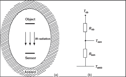
Figure 5 (a) Infrared sensor viewing an object and (b) its equivalent electrical model.
The thermal conductance to the ambient is composed of heat transfer by infrared radiation, by conductance through the nitrogen, and by conductance through the suspension beam(s).
Firstly, let us approximate the heat transferred by infrared radiation from the floating membrane to the ambient. From Equation (6.11), we have that infrared heat transfer will be G″rad = 6 W/K m2, where we should take the surface of the floating membrane twice, since it will be emitting radiation to above and to below the membrane. So, this will give a thermal conduction by radiation of 24 μW/K. In total, the thermal conduction to the ambient is 330 μW/K, so 306 μW/K is transferred by conduction through suspension beams and gas conduction.
Secondly, let us estimate the thermal conduction by the gas in the gap under the floating membrane, which is typically 500 μm (being a standard 4 inch wafer thickness; note that surface micromachining in this case would give a very bad performance). For an area of 2 mm2, and with the thermal conductivity of nitrogen being 26 mW/K m, this conduction will be of the order of 100 μW/K. Let us double this to account for conduction on the sides and to the top of the sensor housing.
Finally, this leaves about 100 μW/K for the conduction through the suspension beams, which corresponds to a thermal resistance of 10 kK/W. For beams with a thickness of 4 μm, that have a thermal sheet resistance of 1.67 kK/W, each of the beams will have a length of 12 squares. Assuming that they run over the full length along the floating membrane, their dimensions would be 2 mm long and 160 μm wide.
(4) Estimate the improvement if the sensor were encapsulated in xenon (κXe = 6 mW/K m) instead of in nitrogen?
By using xenon around the sensor, whose heat conduction is about one-fifth of that of nitrogen, the thermal conductance through the gas is reduced to about 45 μW/K, and this causes the overall thermal conductance to the ambient to be approximately halved. Therefore, the sensitivity of the device is doubled.
Solution to Problem 6.6: thermal modeling
(1) What is the beam's thermal resistance compared to that of the floating membrane?
The thermal sheet resistance of the beam is Rst = 1/(κD) = 1333 K/W ![]() (see Section 6.3.3). Its overall resistance, without the conductance of the argon, is 10 squares times the sheet resistance, 13 kK/W, or a conductance of 75 W/K. According to the Equation (6.23), there will be a loss in resistance due to the conductance by the argon. First, we will calculate the transmission-line constant γ for low frequencies, according to Equation (6.21). For this we must know G″p, which can be found using Equation (6.9), with distance d = 0.5 mm, and κ = 18 mW/K m, and multiplying by two to account for the upper and lower surface of the beam. With these values we find that G″ = 72 W/K m2 and γ = 310/m. Moreover, we find that (γL)2/3 = 0.13, so the effective thermal resistance of the beam becomes 11.6 kK/W. For the floating membrane, we find a thermal conductance to the ambient Gflm equal to G″ × 2 mm2 = 144 μW/K, or a resistance of 7 kK/W. The thermal resistance of the beam is, therefore, twice the thermal resistance between the floating membrane and the ambient through gas conduction.
(see Section 6.3.3). Its overall resistance, without the conductance of the argon, is 10 squares times the sheet resistance, 13 kK/W, or a conductance of 75 W/K. According to the Equation (6.23), there will be a loss in resistance due to the conductance by the argon. First, we will calculate the transmission-line constant γ for low frequencies, according to Equation (6.21). For this we must know G″p, which can be found using Equation (6.9), with distance d = 0.5 mm, and κ = 18 mW/K m, and multiplying by two to account for the upper and lower surface of the beam. With these values we find that G″ = 72 W/K m2 and γ = 310/m. Moreover, we find that (γL)2/3 = 0.13, so the effective thermal resistance of the beam becomes 11.6 kK/W. For the floating membrane, we find a thermal conductance to the ambient Gflm equal to G″ × 2 mm2 = 144 μW/K, or a resistance of 7 kK/W. The thermal resistance of the beam is, therefore, twice the thermal resistance between the floating membrane and the ambient through gas conduction.
(2) How do the thermal time constants of the beam and the overall system compare?
The thermal time constant of the beam follows from Equation (6.24) and, with a thermal square-meter heat capacity Cth = 1.6 MJ/m3 K × 5 μm = 8 J/m2 K, yields a time constant of 14 ms. For the floating membrane, the overall thermal resistance is 4.3 kK/W and the thermal capacitance is 2 mm2 × 8 J/K m2 = 16 μJ/K, the product of which gives the time constant of 69 ms. So, the time constant of the beam can be neglected.
Solution to Problem 6.7: circular thermopiles
What is the sensitivity of the thermopile?
For this we make an estimation of the electrical resistance Rtp of the thermopile by using the equation given for the thermal resistance of a closed membrane, Equation (6.15). The analogy between electrical and thermal models is a two-way street and those familiar with thermal problems can use the solutions to evaluate electrical problems as well. In Equation (6.15) we use the electrical sheet resistance Rse instead of the thermal sheet resistance Rst. We find that for a thermopile consisting of a single strip of 360°, the electrical resistance becomes Rse ln(rin/rout)/2π = 5.5 Ω. Note that the electrical resistance of the thermopile increases with the square of the number of strips, as indicated by Equation (6.32). This holds also true for the case that we divide the full circle into arcs. A resistance of 80 kΩ is allowed, so we can afford (80 kΩ/5.5 Ω)1/2 = 120 strips. These strips will be, at the inner radius, 47 μm wide including the (neglected) separation. If 5 μm separation is usually required, the strips are 10 % narrower at their narrowest end, near the center of the thermopile. In practice, the thermopile will be (5 to 10) % higher in resistance. All this gives a sensitivity of 120 × 0.6 mV/K = 72 mV/K.
Solution to Problem 6.8: chemical microcalorimeter
(1) What is the sensitivity of this microcalorimeter for glucose?
The sensitivity of the thermopile is 72 mV/K. The thermal sheet resistance of the membrane is 1/(150 W/K m × 5 μm) = 1333 K/W ![]() . With Equation (6.24) for homogeneous heating we find, with a heat generation of P″ = 1 W/m2, a membrane of 1.8 mm radius (rrim), and a thermopile with a 0.9 mm inner radius (r), that the temperature increase will be 1.44 mK/W/m2, or 1.44 mK/mmol/l. Multiplying by the thermopile sensitivity gives the overall sensitivity, which is 103 μV/mmol/l. This is a rather high value, and in practice we find sensitivities an order of magnitude lower, because of the thermal conduction and convection of the glucose solution flowing past the sensor. Values of the order of (5 to 10) μV/mmol/l are observed in practice.
. With Equation (6.24) for homogeneous heating we find, with a heat generation of P″ = 1 W/m2, a membrane of 1.8 mm radius (rrim), and a thermopile with a 0.9 mm inner radius (r), that the temperature increase will be 1.44 mK/W/m2, or 1.44 mK/mmol/l. Multiplying by the thermopile sensitivity gives the overall sensitivity, which is 103 μV/mmol/l. This is a rather high value, and in practice we find sensitivities an order of magnitude lower, because of the thermal conduction and convection of the glucose solution flowing past the sensor. Values of the order of (5 to 10) μV/mmol/l are observed in practice.
(2) What is the resolution in a 1 Hz band?
For this we calculate the thermal or Johnson noise un, which is given by the well-known formula un = (4kTRtp)1/2 for a (0 to 1) Hz band. The electrical resistance Rtp of the thermopile is 80 kΩ, and the noise is 36 nV. If we define the resolution to be the signal where a signal-to-noise ratio of 8 exists for easy readout of the results, the electrical signal at resolution is 0.3 μV, and the resolution for glucose is 50 μmol/l, if we take a sensitivity of 6 μV/mmol/l.
Solution to Problem 6.9: self-heating in a resistor
What is the error in the temperature measurement caused by the self-heating of the resistor?
We first calculate the thermal resistance between the resistor and the rest of the chip. Assuming radial heat flow with Equation (6.16), we can find the thermal resistance. Because we are working in a half-space, this value is multiplied by a factor of 2. As the outer radius, we take infinity, as the inner radius, we take a half-sphere with the same area as the resistor surface, which is 625 μm2. The inner radius is given by 2πr2 = 625 μm2, so r = 10 μm. This gives a thermal resistance of 106 K/W. At a dissipation of 100 μA × 100 μA × 3.9 kΩ = 39 μW, the error is 4.1 mK, quite acceptable in many cases. Note that assuming an outer radius of infinity causes a minor error. In comparison with substituting a more practical value of 0.5 mm, which is representative for the chip thickness, this error amounts to only 2 %.
Chapter 7
Solution to Problem 7.1
(1) What is the temperature rise due to self-heating?
According to Figure 7.7(b) the thermal conductance amounts to Gsg ≅ 1.1 × 10⁻³ W K−1. Therefore, a continuous power dissipation P of 1 mW will cause a temperature rise of about P/Gsg = 0.9 K. Increasing the sensor area, for instance by assembling the chip on a flat ceramic substrate or by using flat connecting wires, can reduce this effect. Another excellent way to reduce this effect is explained in the part (3) of this problem.
(2) In the case of single-sided flow the cooling area is only half of what it was before. Consequently, thermal conductance will have only have half of its original value, being 0.55 × 10⁻³ W K−1, which will double the temperature rise.
(3) Calculate the mean temperature rise ΔTmean during a switch-on time of 30 ms.
As a first step we determine the thermal time constant τ. The simplest way is to use the measurement result presented in Figure 7.7(b), which shows that at the specified flow velocity of 1 m/s that τ ≅ 0.6 s. As an alternative this time constant can also been found from the calculation of τ = Cth/Gsg, where Gsg is the thermal conductance calculated in part (1) of this problem and Cth is the thermal capacitance which equals the product of the chip volume and the specific heat. For silicon at 300 K the specific heat amounts to 1.6 MJ K−1 m−3 (see also Chapter 6, Problem 6.6). So that Cth = 0.64 × 10⁻³ J K−1
The temperature rises exponentially with time. However, since the switch-on time is much less than the thermal time constant, the temperature rise ΔT will increase almost proportionally to the time, according to the equation: ΔT(t) ≈ Pt/Cth. With t = 30 ms this yields ΔT = 47 × 10−3 K. During the measurement time the mean rise will amount to half of this value: ΔT ≈ 24 × 10−3 K.
(4) What would be the consequence of doubling the chip thickness for the temperature rise as calculated in part (3) of this problem?
When the chip thickness is doubled the thermal capacitance will also double. Therefore also the mean temperature rise will double. The thermal resistance will hardly be affected by changes in the chip thickness. Therefore, the temperature rise in stationary conditions, as calculated under part (1) of this problem, will hardly be affected.
(5) What is the mean temperature rise in the case of repetitive powering during 30 ms and intervals of 3 s?
The mean power dissipation amounts to Ptm/(ti + tm) = 10−5 W. As a result of this mean power dissipation there will be a mean temperature rise ΔTrep = Pmean/Gsg ≈ 0.009 K. This relatively small effect can be further reduced by enlarging the sensor area as suggested in answer (1).
Solution to Problem 7.2
Calculate the equivalent temperature errors for a 1 % change in Is for the three sensors at 273 K.
For the transistor, from Equation (7.8) the well-known relation for the transconductance gm is found:
This equation shows that a change in Is of 1 % causes a change in V0 (=VBE) of approximately (kT/q) × 1 % = 0.24 mV. By using Equation (4.37) we can calculate the temperature dependence λ of V0. Since at T = 0 K, VBE0 = 1.27 V (mainly related to fundamental physical values), we find that λ = −2.27 mV K−1. Therefore, the equivalent temperature error to be calculated is 0.24 mV/(2.27 mV K−1) = 0.1 K.
For the thermistor we use Equation (7.7) to calculate that R−1dR/dT = −1/(bT2) ≈ 6 % K−1. Because V0 is the linear product of the resistance and the current, a 1 % change in Is is equivalent to a temperature error of 1 %/(6 % K−1) = 0.17 K.
For the Pt resistor it can be found, using Equation (7.4), that R−1dR/dT = R−1Rpt(0){a − 2bt}. When T = 273 K and the values given in Section 7.3.1 are substituted in this equation we get a relative temperature sensitivity of 0.39 % K−1. Consequently, a 1 % change in Is is equivalent to 1 %/(0.39 % K−1) = 2.6 K. This shows that the Pt resistor sensor is much more sensitive to change in the bias current than the transistor or the thermistor. Therefore, Pt resistors should always be used in configurations with (temperature-independent) reference resistors (see Chapter 10).
Solution to Problem 7.3
Calculate the minimum number Nmin of periods of the sensor signal required to measure the temperature.
Since the sensor sensitivity is 0.5 % K−1, the duty cycle varies from 0 to 1 for a temperature range of TH − TL = 200 K. For the minimum measurement time it holds that tmin = Nmintp. When this equation is substituted in Equation (7.24) we get
Substitution of the given and calculated values yields N = 67 (tm ≈ 20 ms).
Chapter 8
Solution to Problem 8.1
Find the effect of the capacitor Cgd on the current i2.
Figure 8.8(b) shows an equivalent circuit model of the floating electrode structure.
(1) Capacitor Cg has no effect on the current i2.
(2) The current i2 is the sum of currents through capacitors Co and C2 and equals:
where s represents the Laplace operator.
The amplitude of the current i2 is given by:
where f represents the frequency of the excitation signal Vm.
Calculate the values of current i2 when the coupling capacitor has a value of Cgd = 1 pF and 100 pF
From Equation (16), it has been found that:
Solution to Problem 8.2
Find the minimum bandwidth of opamp.
As shown in Section 8.6.2, when the capacitance Cp2 and Cint are much larger than Cs, with a required accuracy of 10−5, the unity-gain bandwidth fT of the opamp must satisfy the following condition:
With the given values of the components, it has been found that:
Solution to Problem 8.3
Please see the solution for the Problem 2.2 in Chapter 2.
Solution to Problem 8.4
Calculate the size of the voltage peaks at the output of the integrator.
During the charge phase (T1), the capacitor Cs is charged to a value of VexCs and the capacitor Coff is charged to a value of Vcomp,p–pCoff. At the moment t1, the output of the integrator crosses the threshold level of the comparator. Then, the state of the comparator output is changed and the charge (VexCs + Vcomp,p–pCoff) is transferred to the integrator capacitor Cint, via the switch S3. This charge results in a voltage step at the output of the integrator, which equals:
During the discharge phase (T2), only the capacitor Coff is charged to a value of Vcomp,p–pCoff. At the moment t2, the charge Vcomp,p–pCoff is transferred to the integrator capacitor Cint. This charge results in a step at the output of the integrator:
Solution to Problem 8.5
(1) Calculate the effect of the shunting conductance Gs on the period T of the oscillator shown in Figure 8.16
The charge interval T1 is not affected by the shunting conductance Gs because it is only determined by the charge Vcomp,p–pCoff. The value of T1 is given by Equation (8.10). Because of the shunting conductance Gs, during this phase, the capacitor Cs is charged to a value CsVex/(1 + 2RONGs). Therefore, the discharge period T2 equals:
By summing the results from Equations (8.10) and (20), the period T of the oscillator output signal has been found to be:
(2) When Vcomp,p–p = Vex = 5 V, |Ich| = 5μA, RON = 1 kΩ, Gs = 1 μS, and Coff = 1 pF and Cs = 2 pF, the relative error is:
Chapter 9
Solution to Problem 9.1: Hall device characteristics
(a) Hall coefficient
Equation (9.13): From well known characteristics of electrical properties for the silicon (e.g. http://www.ioffe.rssi.ru/SVA/NSM/Semicond/Si/electric.html#Hall), resistivity versus impurity concentration for Si at 300 K) the doping concentration corresponding to ρ = 1 Ω cm at 300 K is determined, to be ND ≅ 4.5 × 1015 cm−3. At room temperature and such moderate doping level, all donors are ionized, and the density of quasi-free electrons corresponds to that of donors, that is n ≅ ND. Thus
(b) Device resistance
(c) Current
(d) Hall voltage [1]
(e) Absolute sensitivity [2]
(f) Current-related sensitivity [3]
Solution to Problem 9.2: Noise of an integrated Hall device in silicon
The noise and its RMS value depend on the frequency range involved. Given the noise spectral density SN(f), Equation (9.23), the RMS noise can be calculated as:

where f1 and f2 are the boundaries of the frequency range in which the noise is considered.
(a) Static mode
Two kinds of noise can be distinguished: thermal noise and flicker (1/f) noise with a corner frequency of 300 Hz. In the frequency bandwidth of 0.1 Hz to 100 Hz, 1/f noise dominates and thermal noise can be neglected. The noise spectral density can be described by a function
Thus

(b) Mode with implemented spinning current method
The noise spectral density is reduced to the thermal noise, i.e. a uniform distribution over the frequency, described by a constant
Thus

Then, the improvement factor of the spinning-current method on the micro-Hall device can be defined as
Chapter 10
Solution to Problem 10.1
(1) How large is the duty cycle of the output signal?
The current through RCS amounts to (VDD − VDD/2)/RCS = 0.2 μA. During the down-going slope of Vi, the current through RCS is added to Iref. Therefore, the current ICi through Ci amount to 1.2 μA. During the up-going slope of Vi, the current through RCS is subtracted from the reverted Iref. So that the magnitude of the current ICi through Ci amount to 0.8 μA. The ‘down’ time tdown and the ‘up’ time tup are inversely proportional to these currents. Therefore, it holds that
(2) How large is the period time tp of the output signal?
When RCS → infinite, then according to Equation (10.1) tdown = tup, so that for the period time tp,infinite it holds that
where Vx = VDD.
When RCS = 10 MΩ, the charge and discharge currents amount to 1.2 μA and 0.8 μA, respectively (see the previous problem). Substitution of these current values in Equation (10.1) shows that
From Equations (24) and (25), it is found that the relative effect of RCS corresponds to 4.3 %.
Solution to Problem 10.2
How large current iCs during the time interval ti to t2 ?
During the time interval t1 to t2, the output voltage is constant (Vi = Vref). Because

it follows that iCi = 0 A. Therefore, during this time interval, it holds that iCS = −Iref.
Solution to Problem 10.3
(i) How large are the time intervals td,up and td,down?
For the up-going transient of the voltage V2(t) it holds that
where τ = RC. For the moment td,up it holds that V2(t)/VDD = 0.25. Substitution of this value in Equation 27 yields td,up = 0.2878τ. In a similar way, it is found that td,down = 1.386τ.
(2) How large is the error εdc in the measured duty cycle?
For the measured duty cycle Mdc it holds that
where the last term in the right-hand side of Equation (28) represents the error in the duty cycle. On substitution of the calculated values for td,up and td,down and with τ = RC =1 μs, for the error εdc it is found that εdc = 0.0037 = 0.37 %.
Solution to Problem 10.4
(1) For the case that ts = 200 ns, estimate the value of the measurement time tmfor which quantization noise and white noise have equal standard deviations.
There is no correlation between quantization noise and white noise. Therefore for the total standard deviation σtot it holds that:
where σqn and σwn represent the standard deviations of the quantization noise and the white noise, respectively. To calculate the measurement time tm at which σqn = σwn, we can rewrite Equation (10.7) as
where q = ts/√6. White noise is inversely proportional to the square root of the measurement time, which can be explicitly be expressed as:
From Equations (30) and (31), we can find that σqn = σwn for a measurement time tm,eq which equals
According to Equation (10.7), quantization noise decreases proportional with ts. On the other hand, the value of ts does not affect the magnitude of white noise. Therefore, the value of white noise can easily be found from the measurement results at the smallest value, being ts = 14.2 ns. Considering these properties together with Equation (29), it can be concluded that for ts = 14.2 ns and tm = 14 ms (Figure 10.7) the effect of quantization noise is negligible. Therefore, for tm = 14 ms we find that σwn = 0.58 × 10⁻⁴. Substitution of this value in Equation (29) shows that in the case of ts = 200 ns (Figure 10.7(a)) it holds that σqn = 0.815 × 10⁻⁴. Substitution of these values in Equations (30) and (31) gives q = 1.14 × 10⁻⁶ s and r = 6.9 × 10⁻⁶ s1/2. With these values and Equation (32) we find that tm,eq = 27.6 ms.
(2) For the case that ts = 1 ns, estimate the value of the measurement time tmfor which quantization noise and white noise have equal standard deviations.
White noise is not affected by ts, but quantization noise decreases proportionally with ts. In the previous problem it has been found that for ts = 200 ns, q = 1.14 × 10⁻⁶ s. At ts = 14.2 ns, the q value qfast is 14.2 ns/200 ns times smaller than that at 200 ns. From this it is found, that qfast = 0.081 × 10⁻⁶ s. Substitution of this value and the r value in Equation (32) gives tm,eq = 0.14 ms.
From these calculations, it can be concluded that sensor systems similar to that of Figures 10.7(c) and (d) cannot be improved by replacing for instance the asynchronous converter by a high resolution sigma–delta one. Instead of this, to improve the system performance, the white noise of the front-end circuitry has to be reduced.
Solution to Problem 10.5
(1) Calculate the relative error eos caused by the offset voltage Vos.
The full-scale output voltage amounts to ±0.25 % of VS,DC, which corresponds to ±12.5 mV. The relative error caused by the offset voltage amounts to ±8 %.
(2) Calculate the relative error εsw caused by the switch resistances.
The equivalent resistance Rbridge between the terminals A and B, amounts to 1 kΩ. Because of the voltage drop across the switch resistances, the voltage VAB across these terminals amounts to
The voltage drop over the switches causes a relative error, which equals the relative decrease of the voltage VAB and amounts to about 17 %.
Solution to Problem 10.6
Calculate the relative error eT caused by the interconnection of resistance-meter terminals.
By making the interconnection the sensor resistance is connected in series with wire resistance with a total equivalent series resistance of 1 Ω. The corresponding temperature error amounts to 2.5 K.
Chapter 11
(1) Taking into account that fx <fo, the measurement time must be calculated according to Equation (11.13). The answer is 20 ms.
(2) In the first case fx > f0, the measurement time must be calculated according the Equation (11.13), in the second case (fx <f0), according the Equation (11.14). The answers are 40ms and 13.3 ms, respectively.
(3) In order to be neglected, the UFDC's conversion error must be at least in two times less. So, a 0.001 % accuracy for the UFDC should be enough.
(4) The UFDC-1 can exchange accuracy for speed and vice versa. Hence, depending on the measuring conditions and algorithms in the DAQ system, the accuracy of the UFDC-1 can be decreased by up to 1 %. In this case, we will have the minimum possible measuring time. This is useful, for example, for some critical values in order to ensure action of the control system as soon as possible, for example in ABS, when a wheel is blocked. In the case of the maximum possible accuracy, the measuring time will be increased. For, example, such mode can be used in an ABS system at a nominal rotation speed in order to optimize engine performance.
Example: for frequency fx = 25 kHz and reference frequency f0 = 62.5kHz, measuring times at 1 % and 0.0035 % will be 1.64 ms and 457 ms, respectively.
References
2. Schott, Ch., Waser, J.-M. and Popovic, R.S. (2000). Single-chip 3-D silicon Hall sensor, Sensors and Actuators A: Physical, 82, 167–173.
3. Kejik, P., Schurig, E., Bergsma, F. and Popovic, R.S. (2005). First fully SMOS-integrated 3D Hall probe. In Proceedings of the 12th International Conference on Solid-State Sensors, Actuators and Microsystems, 5–9 June, Seoul, South Korea.