2
Interface Electronics and Measurement Techniques for Smart Sensor Systems
Gerard C.M. Meijer
2.1 Introduction
In smart sensor systems, the functions of sensors and their interfaces are combined in an overall design. These functions include sensing, signal conditioning, analog-to-digital conversion, bus interfacing and data processing. Also, functions at a higher hierarchical level can be included, such as self-testing, autocalibration, data evaluation and identification. In many physical and chemical sensors, the information bandwidth is rather small, i.e. much smaller than that of the electronic part of the system. This allows the system designer to use a single electronic system to support many sensing elements, in order to perform multiple measurements. In addition he can use the surplus of available time/bandwidth of the electronic part to improve the system's accuracy, reliability and long-term stability or to lower the power dissipation. This chapter will discuss possible measurement techniques suited to achieve such a system improvement and ways to implement these techniques in smart-sensor-interface circuits. It will be shown how the application of advanced measurement techniques, such as nested chopping, dynamic element matching and autocalibration, can solve the traditional problems of electronic circuits, such as offset, 1/f noise, interference and long-term drift.
The systems under consideration consist of a number of multiplexed sensing elements, sensor-specific front-ends, modulators or converters, and a microcontroller or a digital signal processor (DSP). Such systems appear to fit well in standardized system set-ups, according to the IEEE 1451 standards [1].
This chapter introduces the object-oriented design approach as a very suitable method for rapidly designing low-cost high-performance systems.
Many sensing elements have the problem of cross-sensitivity; i.e. besides their sensitivity for the measurand, they also show an undesired sensitivity for other physical quantities. Moreover, besides the desired electrical output signal, they also show parasitic electrical effects. This chapter discusses how the measurand can be detected selectively, with a high immunity against parasitic effects, interfering signals and parameter drift. A set-up is presented in which the analog sensor signals are converted to analog signals in the time domain, using period-modulated oscillators. The A/D conversion of the time-domain signal can be implemented in the microcontroller or DSP.
To show possible solutions for the implementation of the electronic part of the system, we will present two case studies: a universal sensor interface and a dynamic voltage processor.
2.2 Object-oriented Design of Sensor Systems
System performance can be improved significantly and costs reduced by merging and re-evaluating the functions of sensors, actuators, analog interfacing circuits and digital processors in overall designs. Where technology allows, the system can be implemented on a common substrate or in a single-chip integrated circuit.
In this chapter we will consider sensor systems that are targeted at a cost-driven, medium-volume, industrial sensor market. According to Toth [2], when designing sensor systems, the traditional top-down and bottom-up design approaches have serious limitations. These limitations are due to the interdisciplinary and relatively open character of the sensor subsystems. Consequently, the traditional design methods often require too many iteration steps and result in a long design time and inflexible designs. To overcome these limitations, system designs and specifications should be reused as much as possible. By analogy with a similar design approach in software engineering, Toth refers to this approach as Object-Oriented Design. Figure 2.1 shows a possible hardware configuration resulting from such an approach for a sensor system in which powerful components have been used, such as microcontrollers (μCs), personal computers (PCs) and sensor interfaces (see Section 2.6 and Chapter 10). The availability of memory in the microcontroller makes it possible to collect data over a longer period for a number of sensors. This enables the realization of several important system functions, such as autocalibration, self-testing and the compensation and filtering of undesired signals and effects. As will be explained in Section 2.4, the A/D conversion can be performed in the microcontroller. When the sensor signal is converted to the time domain, using a period-modulator in the transducer interface, microcontrollers can perform this task very well, even without using a built-in A/D converter.
The transducer interface is equipped with front-end electronics for various types of sensors. Sometimes, but not always, it is possible to merge the functions of the sensing element and its interface and to implement them on a single chip, resulting in a so-called ‘Smart Sensor’ (Figure 2.1). In any case, the electrical properties of the front-end electronics should match exactly with those of the sensing elements, taking into account the specific properties, circumstances and nonidealities. In designing a match, object-oriented design will help to speed up design and save costs. To enable this, it is important to recognize the main features and problems of the most common types of sensing elements and sensor systems. In the next sections we will demonstrate this approach for the design of sensor systems with a high accuracy over a wide dynamic range in which the effects of parasitic elements have to be reduced. For other design aspects, such as simplicity and easy prototyping, the reader is referred to Chapter 10.

Figure 2.1 Possible hardware configuration for a smart sensor system
2.3 Sensing Elements and Their Parasitic Effects
There is an extremely wide variety of sensor element. Some of them, such as video sensors, are so special that a discussion of their characteristics is far beyond the scope of this book. In this book, the main interest is focused in sensor systems with a relatively small physical bandwidth, one of less than about 10 kHz. Even with this limitation, there are many problems to be solved. These problems originate from the complexity of the physical/electrical effects and the desire to obtain selective and accurate measurements of specific quantities in presence of many parasitic effects and disturbing signals. In this section, we will discuss these problems and will also present either methods or a strategy to solve them.
2.3.1 Compatibility of Packaging
For almost all types of sensing elements, the packaging problem is a main design issue: to perform its basic function, the contact between the sensing element and the physical or chemical environments should be as good as possible, while, on the other hand, this close contact could be the reason of degradation or damaging of the sensing element. Therefore, the sensing element should be packaged in such a way that it can withstand conditions such as mechanical shocks, high temperatures, a corroding environment, etc. In smart sensor systems, not only the sensing element but also the rest of the sensor system should be well protected, which can considerably complicate the packaging problem. This is the reason why the first smart sensors on the market were those in which this problem could easily be solved. Amongst these sensors are temperature sensors and acceleration sensors. In, for instance, smart temperature sensors, the chip can be packaged in a hermetically closed metal can (Figure 2.2) [3]. With a good thermal design, the temperature inside the package will equalize with the outside temperature, so that the protective packaging does not prevent proper functioning. Also accelerometers have the advantage that a hermetically closed packaging does not disturb its basic functioning. For chemical sensors, however, it is much more difficult to develop a good packaging technique. In Chapter 5 it is shown that conversion of the chemical measurand into a physical one could relax the packaging problem.
Figure 2.2 Photograph of a smart temperature sensor packaged in a TO-18 metal can. After sealing the encapsulation (not shown in the figure) the packaging is tested for gross and fine leakage. (Reproduced by permission of Smartec)
2.3.2 Effect of Cable and Wire Impedances
Provisions must be made to avoid that the impedance of connecting wires and cables affect the measurement. This can be achieved by applying so-called two-port measurements. Figure 2.3(a) shows the well-known four-wire technique, which is applied to measure a low-ohmic sensor impedance Zx. In this case, the series impedances Zs1… Zs4 of the connecting cable do not affect the measured voltage Vsense. The implementation of this technique requires that the interface chip delivers an excitation current and measures the voltage over Zx, using a high-impedance current source and a high-impedance input amplifier, respectively. Figure 2.3(b) shows the dual case, which is applied to measure a high-ohmic sensor admittance Yx with an excitation voltage Vforce and a ‘short-circuit’ current Isense through Yx. The shunt impedances Yp1 and Yp2 of the connecting cables do not affect the measurement. With this technique, it is possible to measure small sensor capacitances Cx, even when connecting cables are used having parasitic capacitances Cp1 and Cp2, which are orders of magnitudes larger than Cx. The implementation of this technique requires the interface chip to deliver an excitation voltage and to measure the current through Yx, using a low-impedance voltage source and a low-impedance input amplifier, respectively.

Figure 2.3 Two cases of the two-port measurement, for the connection of: (a) sensors with a low value of Zx, (b) sensors with a low value of Yx
2.3.3 Parasitic and Cross-effects in Sensing Elements
There exists also a large group of simple sensing elements with electrical properties that can be characterized with a single electrical network element whose main value depends on the physical signal to be measured. Usually, sensing elements have the problem of cross-sensitivity, i.e. besides the sensitivity for the measurand, they also show an undesired sensitivity for other physical quantities, such as temperature, mechanical vibrations, etc. The use of additional sensing elements can provide additional information to improve the reliability and compensate for cross-effects. For instance, the use of additional temperature sensors enables the implementation of temperature compensation. The use of an additional resistance measurement in a thermocouple provides information that can be helpful in monitoring corrosion effects.
In case of cross-effects, the measurand and the undesired physical effects affect the same electrical output parameter Sx. In addition to this, the sensing elements also show parasitic electrical effects, which can have a physical, chemical or an electrical origin and be modeled with an additional parasitic electrical component Sp. For instance, leakage current in a capacitive humidity sensor causes a parasitic resistance Rp to shunt the sensor capacitance Cx (Figure 2.4(a)). Usually, manufacturers do not give a clear specification of this shunting resistance. Moreover, its value shows long-term drift and depends on temperature. Therefore, when designing an electronic measurement circuit for the capacitance Cx, one should take into account the worst-case conditions for the resistor Rp. Applying one of the following measures could solve this problem:
- Using a higher frequency of the excitation signal will result in a decrease of the relative affect of Rp. However, bandwidth limitation of the applied electronic circuits will limit the applicability of this method.
- When a sinusoidal excitation signal is used, a gain-phase analyzer can separately measure the values of Cx and Rp. However the use of sinusoidal signals will increase the system complexity and power consumption.
Figure 2.4 Examples of equivalent electrical circuits modeling some typical sensing elements and their parasitic electrical components: (a)-(d) simple elements; (e) a more complex sensing element
- In case of square wave excitation signals, it is possible to apply a series of measurements at different frequencies of the excitation current. Algorithmic processing of the measurement results will then considerably reduce the effect of the shunting resistance [4]. This method is time consuming but can be performed with a simple electronic circuit.
- Discharging the charged capacitor as fast as possible will reduce the amount of charge loss and therefore the relative effect of the shunting resistance [5].

When a resistive sensor is connected with a long cable wire to the electronic signal processor, the cable capacitance will introduce a shunting capacitor Cp (Figure 2.4(b)). Like the problem discussed above, this problem could be solved by one of the following measurement techniques:
- Using a lower-frequency excitation signal will result in a decrease of the relative effect of Cp. However, to reduce the effect of low-frequency noise and interference, it can be desirable to increase this frequency (see Section 2.3.4)
- When a sinusoidal excitation signal is used, a gain-phase analyzer can separately measure the values of Cp and Rp. However, the use of sinusoidal signals will considerably increase system complexity and power consumption.
Voltage-generating sensors such as thermopiles and pH sensors have a high or even very high internal resistance (Figure 2.4(c)). In this case, extreme care should be taken to minimize the effect of leakage and input currents of the electronic signal processor. Similarly as for current-generating sensors, such as photo detectors (Figure 2.4(d)), the input voltage and input impedance of the electronic signal processor should be as low as possible to reduce the effect of a parasitic shunting resistance.
Figure 2.4(e) depicts a more complex model representing, for instance, an impedance sensor. Such a sensor can be used to measure the electrical properties of a liquid. All of the elements Cp, Rx1 and Rx2 could contain some interesting information about the liquid's properties. Precise measurement of the various elements is challenging. Usually, the elements have such values that they can only be extracted using special frequencies, which complicates measurement. Moreover, the model parameters can show a frequency-dependent behavior, which will make the measurement task even more difficult. In addition to this, the electrical–chemical contact between the solid-state conductors and the liquid will show a complex behavior, which can be modeled by the parasitic impedances Zp. In a first step, during the research phase, a network analyzer can be used to analyze the properties of the set-up for impedance measurements. Usually, such analyzers are large, expensive and power consuming. Possible challenging tasks for the designer of a smart sensor system could include: to minimize the complexity and size of the set-up, to reduce power consumption, and to minimize the system costs. There is a rapidly growing interest in such impedance sensors, which can be applied to measure properties such as: humidity and water content in material, water level, conductivity of liquid, ion concentrations, etc. With impedance sensors the presence of micro-organisms can be detected inside a bottle of milk without opening it. For this application a special interface circuit has been developed which can measure the conductivity of milk inside a bottle using external electrodes [6]. To distinguish between the resistive and capacitive components of the measured impedance, the measurements are performed using various excitation signals and different circuit configurations. As an example, Figure 2.5 shows the measured change of the milk resistance during a test after an infection with Salmonella Typhimurium.

Figure 2.5 Detection of micro-organisms in packaged food products using an impedance sensor: (a) plastic bottle with external electrodes, (b) measured resistance change during a test with Salmonella infection. (After Nihtianov et al. [6])
2.3.4 Excitation Signals for Sensing Elements
In the case of passive sensors (resistive, capacitive or inductive), the interface circuit delivers the excitation signals. This allows the interface designer to select the proper type and size for the excitation signal, with the goal of making the system simple and accurate and of minimizing the power dissipation.
Waveform: With respect to the waveform, the designer can choose between, for instance, dc, square-wave, triangular, sinusoidal or pulsed signals. In general, each of these signals has some advantages and drawbacks, such as:
- Dc signals are simple, but have the problem that there also exist strong disturbing dc signals from which they have to be distinguished. The list of disturbing signals includes, for instance, amplifier offset and offset drift, low-frequency (1/f) noise, interference by the mains, parasitic Seebeck voltages, etc. Another disadvantage of using dc signals could be the occurrence of electrolytic effects. For the latter reason, dc signals may often not be applied.
- Square-wave signals have the advantage that they can be generated with very simple digital circuits (controlled switches), which consume hardly any power.
- Sinusoidal signals have the advantage that, with properly designed filters, an excellent signal-to-noise ratio can be achieved. However, compared to square-wave signals, processing of sinusoidal signals requires circuits with a considerably higher power dissipation and circuit complexity.
- Pulsed signals are rather suited to create selectivity for specific multi-path signals. By applying properly designed time windows, the desired signals can easily be distinguished from reflected ones following a longer transmission path.
Magnitude: In view of the signal-to-noise ratio, the excitation signal should be as large as possible. On the other hand, non-linearity of the sensing elements will limit the optimal magnitude of excitation. Moreover, care has to be taken to avoid undesired electro-physical interaction. For instance:
- Electrical excitation of a resistive temperature sensor causes self-heating, which will cause a measurement error (see Chapter 7). It is the system designer who has to optimize system performance in relation to application-dependent thermal conditions.
- In conductivity sensors, the excitation can cause electrolysis. Therefore, the excitation voltage should be less than the corroding-free potential.
2.4 Analog-to-digital Conversion
In the front-end circuits of conventional systems, the acquired electrical sensor signals are often converted to the voltage domain, so that a standard A/D converter can be used. For a detailed discussion of various types of A/D converter principles and the most suitable types for sensor systems, the reader is referred to ref. [7]. In Chapter 10, we will also discuss an alternative way of A/D conversion that can result in a simplification and improvement of the system.
As an example, Figure 2.6(a) shows a sensor system for a capacitive sensing element Cx, where an off-the-shelf A/D converter is used. The capacitances Cp1 and Cp2 represent the parasitic capacitances of the connecting cables. A drawback of this set-up is that an off-the-shelf A/D converter requires an analog input voltage, which considerably complicates the design of the analog front-end. Accurate conversion of a capacitive signal into a voltage is not easy and would introduce many additional transfer parameters related to component values, biasing quantities and conversion steps. Fortunately, the system can be simplified considerably. Many of the traditional internal functions of A/D converters can be merged with those of the other sub-systems at very low costs.
Figure 2.6 Some possible set-ups: (a) a conventional set-up, (b) a set-up where the A/D converter is implemented in the micro-controller
For instance, the sample-and-hold action, quantization and digital filtering and even ∑–Δ conversion can easily be implemented in the DSP or microcontroller. The small but important front-end part of the A/D converter function can easily be merged with the rest of the front-end circuitry. This yields a set-up as shown in Figure 2.6(b). The capacitance/period converter can be implemented with a relaxation oscillator, whose period varies linearly with the values of the sensing element, so that it generates a period-modulated output signal (Figure 2.7). The sensing element is an integral part of the interface oscillator. In the meantime, this oscillator signal is used for excitation of the sensing element. So no separate excitation generator and no synchronous detector are needed. The A/D converter is partly integrated with the DSP or microcontroller, while another (small) part is implemented in the front-end electronic circuitry. Microcontroller and DSPs are well equipped to measure frequency or time intervals using their internal counters. In the front-end circuitry, both frequency and period modulators can easily be realized. Compared to frequency modulation, period modulation offers the advantage that when autocalibration is used (see Section 2.5.3), the effect of time delay is eliminated. This is because autocalibration removes the effect of all additive errors, including time delay. Compared to the alternative of pulse-width modulation, period modulation has the advantage of having a better immunity against the effects of time constants of the electronic output stage (see Figure 2.7). Therefore, in this chapter we will limit our attention to period modulation. Each period or group of periods can represent a certain measurand. To identify the different periods, we should have one that is shorter than the other ones. Usually the offset measurement is chosen as identification signal (see Chapter 10).

Figure 2.7 Period modulation: the detected signal is immune to the effect of the time constants of the output stage (dotted lines)
Period-modulated signals are analog in the time domain. When these signal are supplied to the timer input of a microcontroller, an internal counter can digitize their period length using asynchronous sampling pulses (Figure 2.8).
In today's microcontrollers, the sampling rate of these counters is in the range of 0.1μs to 1μs. For fast handling of the input signals, the capture register of the microcontroller should be used (see Chapter 12). The quantization noise introduced by the digitization is proportional to the sampling rate and inversely proportional to the period Tx. In the universal transducer interface UTI (see Section 2.6 and Chapter 12) the internal frequency is 50 kHz. The counter acts as an integrator. To lower the quantization noise, an internal frequency divider can be used which reduces the output frequency by, for instance, a factor of 128 or 1024 at the cost of an increased measurement time. When low quantization is needed together with a small measurement time, a high-speed external counter can be used. This solution has been chosen by Gasulla et al. [8] for application in capacitive sensor systems (Chapter 8). Quantization noise can be reduced more effectively by using the principles of ∑–Δ converters. In ∑–Δ converters, oversampling is applied to reduce the noise in the base-band [7]. Next, a low-pass filter removes the increased noise at higher frequencies. For the best noise performance, the order of the filter should exceed the number of applied integrators by at least one. So, in a first-order converter, at least a second-order filter should be used. This filter can be implemented as a digital filter in the microcontroller. Generally, the resolution and measurement speed of the asynchronous sampling system discussed above (Figure 2.8) are slightly better than those of a first-order ∑–Δ converter [9].
Figure 2.8 Analog-to-digital conversion with an asynchronous sampling system
2.5 High Accuracy Over a Wide Dynamic Range
Once the properties of the sensing elements are well known and the desired output signal has been defined, the rest of the electronic interface system can be designed. In this part of the system, the desired measurement techniques have been implemented. The measurement techniques are designed or chosen to get optimum performance according to targeted system specification. In this section, we will discuss advanced measurement techniques that have been developed to obtain a smart sensor system that is highly accurate over a wide dynamic range. To get high accuracy, a variety of measures have to be taken to reduce or eliminate various types of errors, as will be discussed in the next sub-section.
2.5.1 Systematic, Random and Multi-path Errors
With respect to the accuracy of systems, there are three main types of errors:
- Random errors, caused by, for instance, interference, noise and drift. These errors vary randomly each time the measurement is repeated.
- Systematic errors, caused by, for instance, the inaccuracy of system parameters. These errors are reproducible for each time the measurement is repeated.
- Multi-path errors, caused by, for instance, the reflection of pulsed excitation signals.
The random errors can be minimized by filtering in the frequency domain, separating the common-mode and differential-mode signals, application of the three-signal approach and chopping (see Sections 2.5.3 and 2.5.2) and, of course, optimizing the system in terms of noise performance.
There are various ways to reduce the systematic errors, for instance, by calibration and trimming. Traditional calibration consists of comparing the sensor under test to another one of superior quality. For accurate measurements, the data derived from this test are stored in a computer memory or simply written down and used for the remainder of the sensor's life. By trimming, the sensor behavior is altered permanently to make its characteristics match the nominal one as closely as possible, thus eliminating the need for recording individual sensor behavior. Although calibration and trimming are useful ways to improve accuracy, these have a number of shortcomings. For example, calibration and trimming are performed under certain conditions with respect to temperature, supply voltage and time, which can differ from the conditions during actual sensor operation. Moreover, systematic errors may change owing to changes in the environmental conditions and long-term parameter drift. Therefore, the best way to deal with this basic problem is eliminating the influence of all the conversion parameters except those needed for the basic measurements and those that are sufficiently reliable, stable and accurate. In Sections 2.5.2–2.5.4, the basic concepts of advanced techniques to eliminate systematic errors will be discussed.
Multi-path errors occur in systems that use pulses to measure, for instance, time-of-flight, distance, mechanical movement, flow speed, disturbances in material properties etc. The desired signal, which has followed a certain path, is disturbed by reflected ones, which have followed other paths. Filtering in the time domain (time-windowing) can provide an efficient method to obtain selective detection of the desired signal. In the next subsections, a number of the techniques mentioned will be discussed in more detail.
2.5.2 Advanced Chopping Techniques
Chopping in combination with synchronous detection (de-chopping) is a good way to reduce the effects of low-frequency interference and noise, including 1/f noise, offset and offset drift and cross-talk of the mains. A chopper can be implemented with a simple quad of switches (the commutator), which interchange the connecting wires of a signal source with a frequency higher than that of the disturbing signals.
In a conventional chopper, the signal is switched in a +, −, +, −, …. sequence. After amplification in the de-chopper (demodulator), the inverse operation is applied. This de-modulation converts the low-frequency noise and offset to a higher frequency band. With a low-pass filter the high-frequency signals are removed and the amplified version of the desired signal is obtained. Chopping can be considered as a special way of modulation/demodulation with synchronous detection. To improve the chopper performance the signal can be switched in a +, −, −, +, +, −, −, +, … sequence [10]. This means that, after an initial measurement, each time two measurements are performed with the switches in the same position. For interference, this switching sequence results in an improved filtering operation, which can be explained with the following example:
Example 2.1: Let us consider Figure 2.9, which shows a low-frequency interfering signal that is added to a sensor signal (not shown in the figure) that has to be chopped. De-chopping occurs by switching actions of a commutator at the moments (t = ti, i = 1, 2, …). After de-chopping and low-pass filtering, a residual low-frequency component of the interference remains. In case of the conventional chopping method, for a set of four samples, this component εconv amounts to:
In case of the advanced chopping, the residual error εadv is
From Figure 2.9 it can be concluded that εadv ![]() εconv.
εconv.

Figure 2.9 The magnitude of an interfering signal which is de-chopped at the moments ti, (i = 1, 2, …)
In the z-domain, for advanced chopping, the filter transfer function is given by:
with z = exp(jωTmod), Tmod being the modulator period. Equation (2.3) can be transformed into an expression in the frequency domain, which shows that a second-order low-pass filtering for the interfering signal has been obtained.
Unfortunately, the control signals of the switches cause a new problem. Because of the parasitic switching effects of clock-feedthrough and channel-charge injection, even after filtering and demodulation, a residual effect remains. This can be reduced by optimization of the switch design and compensation by the opposite effect of the control signals for n- and p-channel MOSFETs.
Figure 2.10 shows a more basic solution to this problem [11]: in this so-called nested-chopper technique, an additional pair of choppers has been applied, operated at a much lower frequency than the other original pair. For instance, in the circuit of Figure 2.10, the inner commutators are operated at a frequency higher than the 1/f corner frequency (several tens of kiloHertz), while the outer commutators are operated at a rather low frequency (several tens of Hertz). The outer commutators are applied to remove the dc component in the spikes generated by clock feedthrough. The outer switches also have switching effects, but because of the much lower switching frequency, this effect is very small. This technique requires the use of an additional low-pass filter, which can easily be implemented as a digital filter in the software of the applied microcontroller. Introducing a third commutator pair can further extend the basic idea of nested choppers. This third commutator pair can be operated at, for instance, an intermediate medium frequency, somewhere in between the corner frequency of the 1/f noise and the control frequency of the outer chopper, to reduce for instance interference from the mains. Chopping techniques are not suited to reduce the effects of systematic errors caused by, for instance, inaccuracy and drift in the transfer parameters. This type of errors can be eliminated using autocalibration.
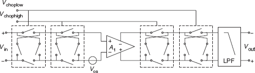
Figure 2.10 Principle of a nested-chopper amplifier
2.5.3 Autocalibration
The undesired effects of transfer-parameter changes can be eliminated in various ways, for instance by autocalibration [12]. During autocalibration, a sufficient number of reference signals Eref,i is measured in exactly the same way as the sensor signal Ex. For a linear system, two reference signals suffice. A signal conditioner converts the sensor signal and the reference signals into, for instance, the time domain, using the period modulators discussed in Section 2.4. The signal conditioner is designed to have a linear relationship between the output signal (time period Ti) and the input signal (the measured signal Ei), so that it holds that:
In this relation, the parameter K represents the system transfer factor, while Toff represents the system offset. In the so-called three-signal measurement, the two reference signals Eref1, Eref1 and the sensor signal Ex are measured sequentially, which results in the three output periods Tref1, Tref2 and Tx,, respectively. Then, the final measurement result is represented by the ratio Mfinal:
Note that this final result is insensitive to both the multiplicative and additive parameters K and Toff of the signal conditioner. It is important to note that the two reference signals Eref1and Eref2 should have the same dimension as the sensor signal Ex. For simplicity, the reference signal Eref1 is often taken to be equal to − Eref2 or to zero. In the latter case, Equation (2.5) is simplified to:
The principles of autocalibration are applied in many of the sensor systems described in this book. Sometimes, full application of this principle is not possible for a complete system. However, even partial application of the autocalibration technique can considerably reduce the amount of system parameters and improve the system performance.
Example 2.2: When measuring a temperature Tx, it is not practical to measure two reference temperatures T1 and T2. Therefore, the temperature can be converted into, for example, a resistor value (see Chapter 7). Then, two reference resistors R1 and R2 can be used to continue the signal processing (Figure 2.11) with the three-signal method described above.

Figure 2.11 Measurement of a resistor Rx (four-wire method). For autocalibration according to the three-signal approach, in addition two reference resistors R1 and R2 are measured
2.5.4 Dynamic Amplification
During autocalibration, three or more signals are processed in an identical way. The system should be linear or well characterized over the full signal range. This poses a problem when the signals are not in the same range of magnitude. As will be shown in this book, in many practical situations, the ratio between a small and a large signal has to be established. This is, for instance the case when the supply voltage Vsupply and the output voltage Vout of a resistive bridge have to be measured in order to determine the relative bridge imbalance Vout/Vsupply (Figure 2.12).
In that case, to achieve high accuracy, the signal processor should have a very high dynamic range. Often such a requirement cannot be met. In these cases the small signals have to be amplified with or the strong signals divided by a scaling factor A, so that all of the signals get the same order of magnitude and the full dynamic range of the signal processor can be exploited. This will yield a better linearity and also a better signal-to-noise ratio for the actual range of the measurand.
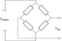
Figure 2.12 Resistive sensing elements in a Wheatstone bridge configuration
An instrumentation amplifier with resistive dynamic-feedback
Suppose it has been decided to amplify the small signals with a factor A, so that the magnitude of the amplified bridge output voltage AVout is closer to that of the supply voltage Vsupply. In that case it will be a design challenge to realize the gain factor A without losing precision. The use of an amplifier with dynamic element matching (DEM) [13, 14] could solve this problem. This is demonstrated in the DEM instrumentation amplifier with dynamic feedback (Figure 2.13). The resistive feedback circuit consists of a chain of K matched resistors. The chain can rotate by addressing of the appropriate switches (only six of them are shown in the figure). The feedback is realized with u, v, and w resistors, respectively. To complete the chain, a resistive load is present that consists of z resistors, where it holds that
By applying force and sense wires, the effect of the ON resistances of the switches S1–S6 is completely eliminated. Rotation of the resistor chain between the two op-amps results in the dynamic feedback. During a full rotation cycle, the feedback has K states. So a resistor that is part of the load will later become part of the feedback. For this reason, the load resistors, which do not affect the gain, are of vital importance for the functionality of the dynamic feedback. The output voltages are converted into the time domain (not shown in Figure 2.13). A microcontroller takes care of digitizing and algorithmic processing. The microcontroller calculates the averaged result of the successive measurements.

Figure 2.13 The principle of a dynamic-feedback instrumentation amplifier. In the figure, only six switches are depicted. Actually, each node of the resistive network is connected with a set of six switches to the amplifier circuit (after De Jong [13])
The average gain G of this amplifier over K successive states equals
Mismatches between the resistors hardly affect the average gain, because these are compensated when the resistors move along the chain. The resistor chain is controlled by a digital-state machine, which addresses the appropriate switches. Every successive state, the chain rotates one position, with a step frequency of about 50 kHz. Control of the resistor chain requires 6 switches connected to each single point between every two resistors, which results in a total of 6K switches. The output voltages are converted into the time domain, where, for instance, a microcontroller takes care of digitization and algorithmic processing.
An instrumentation amplifier with capacitive dynamic feedback
It is also possible to design an instrumentation amplifier with a dynamic feedback loop using switched capacitors [15], [16]. An important feature of this amplifier (Figure 2.14(a)) is that input signals can be handled over the full rail-to-rail common-mode input voltage range. An amplifier with gain factor G requires G+1 identical capacitors. The DEM technique is realized by changing the capacitor positions sequentially in each measurement cycle. This procedure is clarified in Figure 2.14(b). In each cycle, one of the G+1 identical capacitors is in the feedback position of CG+1, while all the others are in the position of CI.
The average value of the amplification factors in a complete cycle is equal to G, for which it holds that

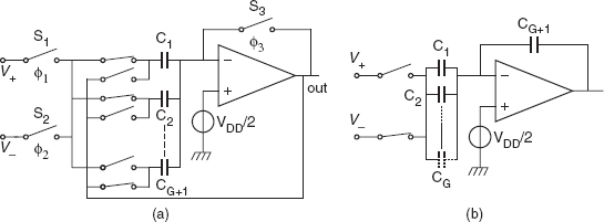
Figure 2.14 (a) A DEM switched capacitor amplifier; (b) simplified drawing of the feedback configuration; after Wang [15]
where ΔG represents the residual second-order error of the mismatch. Just as for the amplifier with resistive feedback, the effect of component mismatches is considerably reduced.
Example 2.3: Suppose that G = 7, and that two of the eight capacitors show a deviation from the nominal value of +1 % and −1 %, respectively. Without DEM, this mismatching causes a relative gain error, which, depending on the capacitor position, can be as large as ±1 %. When applying DEM, the same mismatch would result in a relative error in the average gain of only 29 × 10−6.
2.5.5 Dynamic Division and Other Dynamic Signal-processing Techniques
As for amplifying of the smallest signals, it is also possible to reduce the size of the largest ones, using a dynamic voltage divider [17]. Figure 2.15 shows the principle of such a divider in which a combined resistive/capacitive divider network is used. The divider is realized with NR resistors and NC capacitors, resulting in an accurate division ratio of αd = NCNR.
In this circuit, precautions have been taken to minimize the effect of the ON resistance of the MOS switches on the division ratio. For the resistive part of the divider, this has been achieved by using a high-ohmic input impedance of the amplifier; for the capacitive part of the divider, by using a sample and hold (SH) circuit (not shown in Figure 2.15, but discussed in Chapter 10). The sampling time of the SH circuit should be long enough with respect to the relevant time constants in the divider circuit.
Implementation of DEM techniques requires signal- and data-processing circuits, such as switch controllers, memory and calculation circuits. Microcontrollers are rather suited to perform the functions of such circuits. In addition they can also be used to implement data processing at the level of an overall system design, including averaging or higher-order digital filtering, non-linearity compensation, autocalibration, interference detection, self-testing, etc.
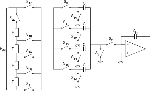
Figure 2.15 A dynamic voltage divider; after van der Goes and Meijer [17]
The case studies presented in the following sections concern sensor systems in which the techniques described above have successfully been implemented.
2.6 A Universal Transducer Interface
As a case study, this section discusses an interface chip called the universal transducer interface (UTI) [18], in which most of the measurement techniques discussed in this chapter have been applied. Figure 2.16 shows an impression of a system designed for multiple sensing elements implemented with UTI chips.
2.6.1 Description of the Interface Chip and the Applied Measurement Techniques
This chip contains a number of front-end circuits, which have been optimized for frequently used sensing elements [10]. Figure 2.17 shows a block diagram of the UTI system.

Figure 2.16 An impression of systems implemented with universal transducer interfaces. Reproduced by permission of G. Wang

Figure 2.17 Block diagram of the UTI system
A number of sensing elements, a reference element, and optionally a biasing element have been connected to the input terminals of the UTI chip. A selector (MUX) connects sequentially each of these elements to one of the specific front ends. The selector (MUX) is controlled by a phase counter, which counts 3, 4 or 5 phases, as discussed further on in this section.
At least three phases are required to implement the autocalibration technique described in Section 2.5.3. The mode-specific front end is connected to a modulator, which consists of a relaxation oscillator. This modulator generates a square-wave output signal, whose period length is proportional to the value of the selected sensing element. To simplify the detection of the period length in the microcontroller and to reduce the effect of connecting wires and (optional) switches between the interface chip and the microcontroller, the output frequency is lowered. This is accomplished with an N-counter, which also triggers the phase counter to select the next measurement phase. Every measurement phase therefore consists of N periods. During the offset measurement phase (time interval Toff in Figure 2.18), the frequency of the UTI output signal is doubled. This enables the microcontroller to recognize the offset period, so that it can be synchronized with the phase counter. As a consequence, the number of periods within a measurement is the number of phases plus one. After 3, 4 or 5 phases (time intervals), a complete measurement cycle has been performed (Figure 2.18).
The oscillator signal generated by the modulator is also used as an excitation signal for the passive sensing elements. This enables synchronous detection of the sensor signals, which increases the immunity against interfering signals. Moreover, it improves the selectivity for the measurand in the presence of parasitic components. With the help of Figure 2.19, this feature can be clarified: Suppose that a square-wave excitation signal causes an output signal of the sensing element, which, due to the parasitic elements, immediately after a 0–1 or 1–0 transition shows undesired transients, spikes, time delay etc. With a sample-and hold circuit the effects of the transient behavior can be reduced. Because the control of the S-H circuit is synchronized with the excitation signal, it is possible to wait until the very end of the time interval of each half period and to take the last moment value for further processing.

Figure 2.18 Output signal of the UTI interface for the case where a complete measurement cycle takes three phases. These phases correspond to three time intervals and four periods
Figure 2.19 Possible wave shape of the distorted output voltage of a front-end amplifier, for a square-wave excitation signal of the sensing element
In fact, this approach demonstrates how selectivity can be obtained with signal processing in the time domain. In addition to frequency-domain signal processing, this technique is quite useful for improving circuit and system performance. In Chapter 10, other examples of time-domain processing will be presented. The frequency of the modulator output signal amounts to several tens of kiloHertz. Depending on the mode applied and after division, the output frequency is in the range of a few tens to a few hundreds of Hertz. Note that the division does not affect the excitation signal.
The modulator and the front-end circuit for capacitive modes
A main part of the interface is the modulator. We will shortly discuss the operation of this modulator for the case that it is connected to the front-end circuit for capacitive sensors (Figure 2.20) [19]. The circuit shown in Figure 2.20 is used to determine the relative value of a sensor capacitor Cx with respect to a reference capacitor Cref. These capacitors have one common electrode, thereby requiring three IC pins to connect the capacitors to the interface chip. In some modes, up to four capacitors and one reference capacitor can be connected, thereby requiring six pins. These pins are denoted A, B, C, D, E and F. The pins are also used in other sensor applications, having different functions for the different applications.
The modulator output controls the switches S1 and S2, so that a square-wave excitation voltage is generated controlled over the selected capacitor Cx or Cref. This results in a square-wave output voltage for operational amplifier OA1, which is operated in its linear region. The amplitude of this output voltage is proportional to the value of the sensor capacitors Cx or Cref. At the end of each half period, the capacitor Cs samples the magnitude of the square-wave output voltage of the front-end amplifier. After that, the charge of Cs is dumped into the integrator capacitor Cint. This charge is removed by integrating the current Iint. As soon as the integrator output voltage exceeds the comparator reference voltage, the comparator switches into another state, starting the next step of the measurement. This relaxation process results in a periodic square-wave output signal of the comparator. The period length of the output signal is linearly related to the values of the sensor capacitors Cx or Cref. To keep the relaxation oscillator running, even when Cx = Cref = 0 pF, an offset capacitor Co2 is used. Another offset capacitor Co1 is used to create a time interval for sampling the output voltage of OA1 with the capacitor Cs [20], [21]. A more detailed discussion on the operation of this circuit is presented in ref. [19].

Figure 2.20 Principle of the UTI system for capacitive-sensor modes
The three-signal autocalibration technique has been implemented in the following way: During the signal-measurement phase, the capacitor Cx is selected, during the reference phase, the capacitor Cref is finally selected, and none of these two is selected during the offset phase.
The capacitors are measured according to the two-port technique shown in Figure 2.3(b) : the transmitting electrode is driven from a low-ohmic voltage source and the receiving electrode is connected to virtual ground (terminal A of the interface chip).
Also the advanced chopper technique has been implemented. This makes the interface output signal rather insensitive to 1/f noise. This is achieved by modulating all relevant electrical signals at a frequency that is higher than the corner frequency of the 1/f noise. Because of this measure, it has been possible to implement the interface chip with low-cost CMOS technology, without problems caused by the strong 1/f noise of CMOS transistors.
The sampling capacitor and the charge-to-period converter (Figure 2.20) of the interface chip belong to the UTI core, which is used in all modes. For the measurement of other types of sensing elements, the input circuitry is slightly modified, as discussed now.
The front-end circuit for resistive modes
The interface adapted for the measurement of platinum resistors is shown in Figure 2.21. A reference resistor Rref is placed in series with the platinum resistor Rpt. To avoid overload of the integrator amplifier, the value of Rbias is selected such that the amplitude of the voltages across Rpt and Rref is smaller than 0.5 V for VDD = 5 V. With the proper choice of Rbias, it is also possible to limit the current through Rpt and therefore self-heating of this temperature sensor (see Chapter 7, Section 7.2.4). The voltages Vref and Vx are measured during the reference and signal phase. These voltages are sensed according to the two-port measurement technique, shown in Figure 2.3(a). The current Ipt is a chopped square-wave ac current, which enables the reduction of low-frequency interfering signals. Since the amplitude of Ipt is almost independent of Rpt, the resolution achieved is almost constant over the entire temperature range of Rpt. The microcontroller calculates the temperature of the platinum resistors by means of a look-up table or by solving an equation.

Figure 2.21 Set-up of the interface for measuring a platinum resistor
The front-end circuit for thermistor modes
The interface adapted to the measurement of thermistors is shown in Figure 2.22. A reference resistor Rref is placed in series with the thermistor Rth. A chopped voltage with an amplitude of 0.08 VDD drives the series-connected resistors. This way of driving strongly linearizes the nonlinear behavior of the thermistor and results in a rather constant resolution over a wide temperature range, according to the method explained in Chapter 7, Figure 7.11.
The microcontroller calculates the thermistor temperature, which is the measurand.
The front-end circuit for bridge modes
The interface adapted for the measurement of resistive bridges is given in Figure 2.23. The resistive bridge consists of four resistors Rb, of which minimally one is sensitive to a physical signal, resulting in a relative resistive change Δ. Two modes for two ranges of the bridge output voltage are available: For large output voltages, the bridge output voltage is directly sampled by the four sampling capacitors Cs/4 in parallel. When the maximum value of the bridge output voltage Vx is below a certain level, Vx is amplified 15 times. Next, this voltage is sampled by the four capacitors Cs/4 in parallel. The amplifier has a very accurate gain based on the dynamic-element-matching technique and needs no calibration (see Section 2.5.3). During the reference measurement phase, the voltage Vref across the bridge is divided into eight almost equal parts (according to the principle discussed in Section 2.5.5), which are sampled by a single capacitor Cs/4. Therefore, the realized on-chip voltage divider effectively divides Vref by 32 (see Section 2.5.5). This division ratio is also very accurate and needs no calibration. The voltages are measured according to the two-port technique of Figure 2.3(a). Furthermore, the principle of advanced chopping (see Section 2.5.2) has also been applied.
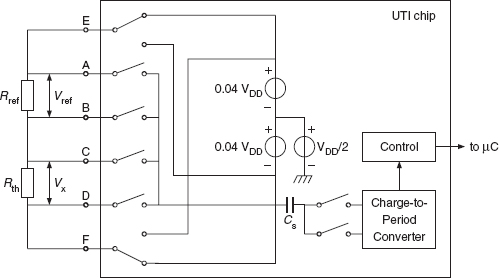
Figure 2.22 Set-up of the interface for measuring thermistors
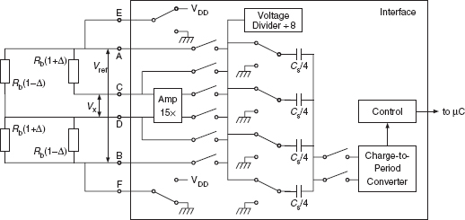
Figure 2.23 Set-up of the interface for measuring the imbalance of a resistive bridge

Figure 2.24 A photomicrograph of the realized sensor interface. The minimum gate length of the applied CMOS process is 0.7 μm. The die measures 5.5 mm2. (Reproduced by permission of Smartec)
2.6.2 Realization and Experimental Results
The UTI chip has been realized in a 0.7 μm CMOS process (Figure 2.24). After selection of one of the 16 application modes [18], this chip provides interfacing for:
- Capacitive sensors in various ranges from (0 to 2) pF up to (0 to 300) pF,
- Single or multiple platinum resistors, for instance of the type Pt100, Pt1000, with externally adjustable biasing current,
- Thermistors with a 0 °C value in the range of 1 kΩ to 25 kΩ, with a provision for linearization,
- Various types of resistive bridges in the range of 250 Ω to 10 kΩ with maximum imbalance ±4 % or ±0.25 %, with current or voltage supply,
- Potentiometers.
In addition to the application modes the interface offers:
- A test mode. This mode is used to check the nonlinearity of the signal-to-time conversion of the interface.
- A selection mode for slow or fast measurement. This selection sets the number of periods N within one measurement phase to 256 or 32, respectively.
- A power-down (chip-enable) mode. When in power-down mode, the current consumption is reduced to a very low level (1 μA) and the output of the interface becomes floating. It is therefore possible to place several interfaces in parallel and connect the outputs together in a wired-OR configuration.

Figure 2.25 Capacitive resolution in the (0 to 2) pF range versus the measurement time
Because of the large number of different modes, the interface can only be characterized with reference to many different measurements results. In this chapter, only for the capacitive modes, some important measurements results have been presented. More information can be found elsewhere [18, 19, 21].
Figure 2.25 shows the measured resolution for capacitive sensors in the measurement range (0 to 2) pF versus the measurement time. To enable this measurement, we bypassed the internal period and phase counters by external ones, which were controlled by the microcontroller itself. Thus it was possible to realize measurement times in the range from 1ms to 3s. The resolution for short measurement times is mainly due to quantization effects. In this range, the resolution is inversely proportional to the measurement time Tmeas (see Chapter 10). For longer measurement times, the electronic noise dominates and the resolution becomes inversely proportional to Tmeas0.5 (Cp = 30 pF) (see Chapter 10).
Usually, in case of a real sensor system, the sensor capacitors are connected to the interface chip with a shielded cable. The parasitic capacitance of this cable, which is about 100 pF/m, causes a parasitic capacitance Cp at input terminal A (see Figure 2.20) of the UTI chip. This capacitor affects some important features of the UTI system. Figure 2.26 shows the measured capacitive resolution in the (0 to 2) pF range versus the parasitic input capacitance Cp of the common electrode (Figure 2.20). If Cp increases, so will the noise-voltage amplification in the input stage. However, at the same time, the bandwidth of the input stage reduces linearly. It can be shown that, because of these effects, the resolution is proportional to Cp0.5. This is confirmed by the measurement results shown in Figure 2.26 for a 100 ms measurement time. With small sensor capacitances it is very difficult to test the absolute accuracy of the system. This is partly because for small capacitor values, precision components hardly exist. Even if such precision capacitors could be fabricated [22], the parasitic capacitors in the interface input would introduce additional errors.
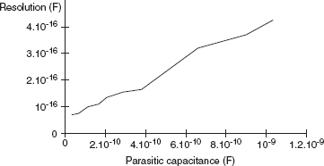
Figure 2.26 Capacitive resolution in the (0 to 2) pF range for a measurement time of 100 ms, versus the parasitic capacitance Cp at the common electrode
Example 2.4: The parasitic capacitances between the pins of an integrated circuit are in the range of a few tenths of a picofarad and vary from pin to pin. In addition the connecting wires also add parasitic capacitance, which makes it very difficult to perform an accuracy test with a precision that equals the resolution of, for instance, 50 aF.
Fortunately, features that are difficult to test are seldom of interest for the user. Conversely, features that are important for practical applications can usually be well tested, provided that sufficient care is taken. One such feature is the nonlinearity of the system. Even with small capacitor values, the nonlinearity of the system can be tested. For these tests, using autocalibration, four phases instead of three are applied. During these phases, in addition to the offset capacitor Coff, the capacitors C1, C2 and the sum of these capacitors C1+C2 are measured. To be sure that during a complete measurement cycle of four phases the parasitic capacitors have identical values, during selection, nothing is changed in the position of the capacitors. The phases are selected by switching on or off the excitation signal, without changing the impedance level at any of the capacitor terminals. This can easily be done using a digital multiplexer [23]. During the four phases, the corresponding periods of the UTI output signal are Toff, TC1, TC2 and TC1+C2, respectively. The nonlinearity λ is found with the equation
For a perfectly linear signal-to-time conversion, the nonlinearity λ is zero. To make this test highly accurate, high-quality capacitors should be used. Teflon capacitors are rather suited because of their very small dielectric absorption. Figure 2.27 shows the measured nonlinearity for Teflon capacitors with a value of about 1 pF connected to the UTI input terminals. During the nonlinearity test, the parasitic capacitor has been simulated with a discrete capacitor.

Figure 2.27 Nonlinearity for capacitive measurements in the (0 to 2) pF range
Table 2.1 Measurement results for some of the 16 application modes

In addition to the experimental results for the capacitive sensors, Table 2.1 shows a summary of experimental results for some of the other 16 application modes. More test results for, for instance, the sensitivity to interfering signals and the accuracy for the other application modes can be found elsewhere [19].
In Table 2.1, the range of the resistive bridges refers to the range of the output voltages. For the resolution of the resistive temperature sensors, in addition to the voltage over the temperature-sensing resistor, the corresponding error of the temperature measurement has also been given.
2.7 Summary and Future Trends
2.7.1 Summary
In the smart sensor systems discussed in this chapter, measurement techniques have been presented that can be implemented with a limited number of low-cost, low-power integrated circuits. The applied techniques enable selective detection of the measurand with a high immunity against parasitic effects of the sensing elements and their connecting wires. The application of synchronous detection, autocalibration and advanced chopping results in a high accuracy, including a high immunity against interfering signals, 1/f noise and parameter drift. Techniques have been presented to increase the dynamic range of the sensor signals. These include the use of dynamic amplifiers and dynamic dividers.
As a case study, we have discussed the application of the measurement techniques in a general-purpose sensor interface. This interface has been designed for capacitive sensors, platinum resistors, thermistors, resistive bridges and potentiometers. Together with a microcontroller, the interface chip enables rapid and easy prototyping of sensor systems. The applied measurement concepts include: the three-signal technique (a continuous autocalibration technique that eliminates offset and gain errors of the interface circuit), indirect A/D conversion based on the use of a first-order oscillator, dynamic voltage division, dynamic element matching, advanced chopping, synchronous detection and two-port measurement techniques. The interface chip has been implemented using low-cost 0.7 μm CMOS technology. Owing to the measurement techniques applied, the effects of traditional nonidealities of CMOS circuits have been eliminated, such as 1/f noise and component mismatching. The system accuracy is in the range of (10 to 15) bit, with a resolution up to 16 bit. The measurement time is in the range (1 to 100) ms. Calibration of the electronic part is not required.
2.7.2 Future Trends
The developments in interface electronics and measurement techniques are driven by the technological developments in mixed-mode circuit design. Especially CMOS technology enables combining analog and digital signal processing on single chips. The availability of on-chip memory allows on-chip data processing, which will make interface electronics smarter and reduce the data rate and power consumption. Standardization of output signals of sensors and sensor interfaces will enable rapid system development. The development of universal sensor interfaces with front-end circuitry for a wide variety of sensing elements will simplify the development of novel sensor systems and help designers implement reliable and high-performance measurement techniques.
In addition to features related to speed and accuracy of the sensor systems, the reliability of these systems will be of the highest importance. Using concepts for multiple-sensor systems the reliability can be improved by design. For instance, the reliability of a sensor system for measuring of temperatures with thermocouples can be improved considerably by monitoring the thermocouple resistance. Because aging effects and drift are significantly correlated with thermocouple resistance, an increase of this resistance can be used as a signal to replace the thermocouples.
Real-time and high-speed processing of the stream of sensor data will pose another challenge for future developments: Future sensor systems will be adaptable, with real-time optimization of their features depending on the specific conditions. This adaptation is only possible with real-time processing of the sensor data. In this way there will be a merging of signal and data processing. Designers practicing ‘learning from nature’ methods will develop sensor systems, which resemble the sensor systems of animals and human beings more and more closely, with artificial eyes and ears adapting to the specific conditions, and sensors and muscles working together, responding to signals generated in central processors. Such sensor systems can only be developed in an overall design approach, where software and hardware engineers work closely together for common purposes.
Problems
2.1 Effect of cables and wires connected to a sensing element (see Section 2.3.2)
(a) A sensor capacitor Cs = 1 pF is connected to the front-end amplifier of a sensor-interface circuit, according to the circuit diagram of Figure 2.28(a). Each of the two shielded cables has a length of 1m and a parasitic capacitance of 100 pF/m. The excitation voltage Vexc is a square-wave signal with a peak-to-peak value of Vp-p = 10 V. The amplifier is operated in its active (linear) region (the biasing circuits are not shown in the circuit diagram). The amplifier may be considered as being ideal with an infinite gain and infinite bandwidth. Answer the following question: What is the shape and magnitude of the amplifier output voltage V0?

Figure 2.28 Effect of connecting cables for capacitive sensors (a) with a two-port connection; (b) with a one-port connection
(b) In some applications, the sensor capacitors are grounded, so that only one terminal is available for external connection. For such an application, the circuit is modified to that shown in Figure 2.28(b). The excitation voltage is the same as mentioned before. What is the shape and magnitude of the amplifier output voltage V0 for this modified circuit configuration?
2.2 Parasitic resistors shunting a capacitive humidity sensing element (see Section 2.3.3)
A capacitive humidity sensor with a capacitance Cs and a leakage resistance Rleak (Figure 2.29(a)) is connected to the front-end circuit of a sensor-interface circuit, according to the circuit diagram of Figure 2.29(b). The excitation voltage Vexc is a square-wave signal with a peak-to-peak value of 1Vp-p and a frequency of 50 kHz. The amplifier is biased in its active region and may be considered as being ideal, with infinite gain and bandwidth. The shape of the amplifier output voltage Vo is shown in Figure 2.29(c).
(a) The effect of the shunting resistor causes the voltage rise Vrise (Figure 2.29(a). Find by calculation the magnitude of this voltage rise.
(b) The output voltage Vo is sampled at the end of each half-period, just before the next transient. At t = t2 this yields the value Vo(t2). Calculate the relative error in this sample, as compared to the ideal value Vo, ideal for the case where Rleak → ∞.
2.3 Time constants in a chopper configuration for a high-ohmic voltage-generating sensor (see sections 2.3.3 and 2.5.2)
A thermopile sensor with an internal resistance Rs = 50 kΩ generates a dc output voltage Vs. This voltage is chopped using a switch S1, which is operated at a frequency f = 50 kHz (Figure 2.30(a)). The input capacitance Cp = 20 pF of a front-end amplifier (not shown in the figure) causes the output voltage Vch to deviate from the ideal voltage Vch, ideal. Both voltages are depicted in Figure 2.30(b). The voltage Vch is sampled at the end of each half-period, just before the next transient. Calculate the relative error ΔVch/Vch of the voltage samples.

Figure 2.29 The effect of the leakage resistor of a capacitive humidity sensor: (a) electrical model of the sensing elements, (b) circuit diagram of the front-end amplifier, (c) the output voltage Vo versus the time

Figure 2.30 Chopper for a thermopile sensor: (a) circuit diagram; (b) output voltage Vch versus the time
2.4 Dynamic amplification with resistive feedback (see Section 2.5.4)
The dynamic feedback amplifier of Figure 2.13 (Section 2.5.4) contains z resistors at the amplifier output. These resistors do not contribute to the gain but consume energy current. Why are they needed?
2.5 Dynamic amplification with capacitive feedback (see Section 2.5.4)
In the circuit of Figure 2.14(a), a switch S3 can be found in the feedback network of the amplifier. Why is this switch needed?
References
1. IEEE (1997). IEEE Std 1451.2, Standard for a Smart Transducer Interface for Sensors and Actuators – Transducer to Microprocessor Communication Protocols and Transducer Electronic Data Sheet (TEDS) Formats, IEEE, New Jersey, USA.
2. Toth, F.N. (1997). A design methodology for low-cost high performance capacitive sensors, PhD Thesis, TU Delft.
3. Smartec (2006–1). www.smartec.nl, Data sheet of Temperature sensors.
4. Li, X. and Meijer, G.C.M. (2000). Elimination of shunting conductance effects in a low-cost capacitive-sensor interface, IEEE Transactions on Instrumentation and Measurement, 49, 531.
5. Li, X. and Meijer, G.C.M. (2002). An accurate interface for capacitive sensors, IEEE Transactions on Instrumentation and Measurement, 51, 935.
6. Nihtianov, S.N., Shterev, G.P., Iliev, B. and Meijer, G.C.M. (2001). An interface circuit for R-C impedance sensors with a relaxation oscillator, IEEE Transactions on Instrumentation and Measurement, 50, 1563.
7. Jespers, P.G.A. (2001). Integrated Converters, Oxford University Press, Oxford.
8. Gasulla, M., Li, X. and Meijer, G.C.M. (2005). The noise performance of a high-speed capacitive-sensor interface based on a relaxation oscillator and a fast counter, IEEE Transactions on Instrumentation and Measurement, 54, 935–939.
9. Van Der Goes, F.M.L. and Meijer, G.C.M. (1996b). Sigma-delta versus oscillator-based converters in low-cost accurate sensor systems. In IEEE IMTC ‘96, Brussels.
10. Van Der Goes, F.M.L. and Meijer, G.C.M. (1997). A universal transducer interface for capacitive and resistive sensor elements, Analog Integrated Circuits and Signal Processing, 14, 249–260.
11. Bakker, A., Thiele, K. and Huijsing, J.H. (2000). A CMOS nested-chopper instrumentation amplifier with 100-nV offset, IEEE Journal of Solid-State Circuits, 35, 1877–1883.
12. Meijer, G.C.M. and van Herwaarden, A.W. (1994). Thermal Sensors, IOP, Bristol, UK.
13. de Jong, P.C. (1996). Dutch Patent application, 1002732.
14. de Jong, P.C., Meijer, G.C.M. and van Roermund, A.H.M. (1998). A 300 °C dynamic-feedback instrumentation amplifier, IEEE Journal of Solid-State Circuits, 33, 1999.
15. Wang, G. (2000). Dutch Patent Application, 1014551.
16. Wang, G. and Meijer, G.C.M. (2000). Accurate DEM SC amplification of small differential-voltage signal with CM level from ground to VDD. In SPIE2000, Newport Beach, USA.
17. Van Der Goes, F.M.L. and Meijer, G.C.M. (1994). A simple and accurate dynamic voltage divider for resistive bridge transducers. In IEEE IMTC/94, Hamamatsu, Japan.
18. Smartec (2000–2). www.smartec.nl, Data sheet Universal Transducer Interface UTI.
19. Van Der Goes, F.M.L. (1996). Low-cost smart sensor interfacing, PhD Thesis, TU Delft.
20. Van Der Goes, F.M.L. and Meijer, G.C.M. (1996a). A novel low-cost capacitive-sensor interface, IEEE Transactions on Instrumentation and Measurement, 45, 536–540.
21. Smartec (2004–2). Interface UTI.
22. Toth, F.N., Bertels, D. and Meijer, G.C.M. (1996). A low-cost, stable reference capacitor for capacitive sensor systems, IEEE Transactions on Instrumentation and Measurement, 45, 526.
23. Toth, F.N. and Meijer, G.C.M. (1992). A low-cost, smart capacitive position sensor, IEEE Transactions on Instrumentation and Measurement, 41, 1041.
Smart Sensor Systems Edited by Gerard C.M. Meijer
© 2008 John Wiley & Sons, Ltd