12
Microcontrollers and Digital Signal Processors for Smart Sensor Systems
Ratcho M. Ivanov
12.1 Introduction
In addition to a wide variety of other applications, microcontrollers (MCUs) and digital signal processors (DSPs) are also very suited for application in data-acquisition systems, control systems, and smart sensor systems. The design of a smart sensor system starts with selecting the transducers needed to evaluate the physical quantity to be measured. Unfortunately, transducers rarely, if ever, output the exact electrical parameter, or value, suitable for direct input to a microcontroller. Therefore, the main part of the effort in designing smart sensor systems is related to the analog and digital signal processing needed to acquire suitable input signals for the MCUs and DSPs.
DSPs and MCUs are programmable processors which can utilize software programs to achieve different functions and features. It is often required to convert analog signals to digital ones, using analog-to-digital converters to do digital processing and to interface to data-acquisition systems and control systems. In addition, it is often required to implement smart data processing, such as autocalibration, self-testing, and other advanced features, which can easily be performed because of the substantial computational power of the digital processors. For an optimal system design, the processor must be embedded in the overall sensor system. For real-time signal processing, DSP is rated best or exceptional in terms of performance. However, the microcontrollers use less power and are less expensive.
For MCUs and DSPs used in sensor systems, the main specific requirements are:
- Low power consumption;
- High performance and computational power;
- Timing measurement resources;
- Analog-to-digital, digital-to-analog converters, and analog comparators;
- Networks and LCD interfacing;
- In-system programmable flash and code protection;
- Availability of development tools;
- Low cost.
Regarding the output sensor voltage, analog as well as digital outputs can be found. Often, sensors with a digital output can be directly connected to standard interfaces such as SPI, I2C, etc., while the output signals of the analog sensor must first be converted to digital before it is digitally processed. A third group of sensors offers output signals that are pulse width modulated (PWM). For the latter group, the conversion to digital signals is performed with time measurement resources.
The problem, therefore, boils down to selecting the appropriate MCU or DSP for the specific application, as part of a smart sensor system. Network capability should be considered together with the respective types of local networks for the smart sensor systems. For portable instruments, the power consumption is very important. Furthermore, in the case of a high accuracy PWM measurement, such as that required for a universal transducer interface with a period-modulated output signal (see Chapter 10), an MCU with high internal counter frequency needs to be chosen. This will yield a low quantization error value.
Depending on the system designed, some of the requirements are contradictory, and a compromise needs to be made, according to what is most essential.
12.2 MCU and DSP Architectures, Organization, Structures, and Peripherals
There are two main types of architectures: Harvard and von Neumann (Figure 12.1). The Harvard architecture has its program memory and its data memory located in separate memory spaces, which are accessed from separate buses. In the von Neumann architecture the program and data memories are located in the same memory space, using the same bus. To execute an instruction, a von Neumann machine must make one or more accesses across the data bus to fetch the instruction. The data can be fetched, operated on, and possibly written using the same data bus again. With the Harvard architecture, the instruction is fetched in a single instruction cycle. While the program memory is being accessed, the data memory is on an independent bus and can be read or written. These separate buses allow the execution of an instruction while the next one is being fetched. Devices with the Harvard architecture are faster but more complicated than those with the von Neumann architecture. Figure 12.2 shows a block diagram of a computer.

Figure 12.1 The Hardvard and von Neumann architectures

Figure 12.2 The block diagram of a computer
The central processing unit (CPU) performs both arithmetical and Boolean logical operations. Some machines may be provided with separate internal implementations that separate the logical operations from the arithmetical ones and place the results in separate accumulators. Usually the CPUs can handle data with the size of 8, 16, or 32 bits. The computational power, which we need, must be known when selecting a CPU. When selecting a CPU with more bits, the system will have more computational power, but it will also have the drawbacks of higher complexity and higher cost. Selecting the MCU or DSP is a complicated matter and deserves careful attention. Nowadays, there is a large variety of 8-, 16- and 32-bit microprocessors. Modern technologies enable the production of competitively priced 16-bit and 32-bit CPUs. This fact has a major impact on lowering the cost of smart sensor systems.
The different MCUs and DSP have different architectures that influence their performance and computational power. The Harvard architecture and the presence of more than a single data and address bus usually assure higher performance, but also increase the system complexity. For most of the digital processing algorithms, the availability of a multiply-and-accumulate (MAC) module in a DSP gives a large advantage. However, this requires additional silicon area. The availability of RISC (reduced instruction set) leads to shorter instruction execution time, but a larger program code as well. Because of these tradeoffs, on the market there is an enormous variety of MCUs and DSPs with different architectures and instruction sets. The designer should always search for a compromise between different requirements to find the best fit for their specific application.
The program memory can be of the type read only memory (ROM), electrically programmable read only memory (EPROM), or nowadays flash memory. In the past, the program memory used to be of the ROM type. This has the drawback that programming is only possible during the manufacturing of the integrated circuits (IC, ASIC), which includes the memory. As a result, any error, no matter how small it is (even a single bit), makes the circuit unusable. The EPROMs have the advantage that reprogramming is possible. However, reprogramming requires special programming tools and ultraviolet-light erasing devices. The EPROMs are manufactured in two versions: one with a quartz window (that can be programmed multiple times) and another one with a plastic body and one-time-programming (OTP) capability. The EPROMs with a quartz window are much more convenient but are more than three times as expensive as the OTP EPROMs. In today's microcontrollers, on-chip flash memory is often used to store the embedded program.
Memories of this type can be reprogrammed multiple times without the erasing process requiring any special devices. Programming can be performed in a few different ways, which depends on the type of microcontroller. The on-chip flash memory's main advantage is that it can be directly programmed on location in the applied system. This feature facilitates a more accessible testing and bug-fixing procedure for the software. Some microcontrollers are also equipped with on-chip data flash memory.
As a part of the MCU and DSP, random access memory (RAM) is a read/write memory that is used to save data during computation and process controls. For systems in which the executed program is read from flash memory, the RAM memory does not need to have a large capacity. The RAM is used to gather information as a working space for the program but it is very rarely used to hold the program code. Its capacity ranges from a few tens of bytes up to few kilobytes. When choosing a microcontroller it is rarely the RAM that it is the heaviest component, but in some applications which gather information it may be an important factor. The RAM is byte or word organized – the latter in the case that the CPU is not an 8-bit one. For the CPU, it is common to have instructions that work with both bytes and words. This CPU capability makes the use of the RAM more efficient. There are microcontrollers that allow the use of a standalone power supply for its RAM so that batteries can be used to preserve the memory contents even in the case of a power failure. Thus, after the system's restart it can continue gathering information without losing any data. Also, the values of the coefficients stored in this memory will be preserved.
The clock and timer system is a very important part of the system. Because smart sensor systems operate in real time, they requires a stable clock. For the CPU the clock generator is necessary to execute instructions. In microcontrollers available nowadays, it is built in. The manufacturers aim to have their clock generators work with both low and high frequencies. The low frequencies are used to lower power consumption and the high frequencies are used to increase computational power. The timers are part of the microcontroller's periphery. In smart sensor systems they are essential for measurement timing and time interval sampling. Sometimes, a real-time clock is required to determine exactly the moment at which an event happened.
Digital peripherals are essential for controlling the MCU and DSP inputs and outputs that are connected to sensors and actuators. In these peripherals, different interfaces for communications are also found. Regarding the digital inputs and outputs, parallel ports are the most popular. Most of the peripherals operate in byte format. Commonly, via a few registers, the parallel ports are structured in such a way that they can be either managed and configured as inputs or outputs or serviced by interrupts, etc. Some of the parallel ports are designed for direct control of light emitting diodes (LEDs). Different manufacturers can provide many other parallel port features. Another part of these peripheries is the serial interface, which can be synchronous or asynchronous. In sensor systems, this interface enables connection to a network and communication with a host computer.
The analog peripherals often include analog-to-digital converters (ADCs), digital to-analog converters (DACs), as well as analog comparators. Initially, only 8-bit ADCs were being integrated, but in recent years there are MCUs with 12-, 14- or even 24-bit ADCs included. For sensor systems, this happens to be very important. Currently, in some of the MCUs, even programmable operational amplifiers are being built in so that sensor signals can be amplified and transformed by the MCU itself. There are MCUs with integrated analog comparators. Their applications vary from power supply control to integrating in circuits for transformation and measuring resistors and capacitors values. They are designed in such way that they easily control an application, for instance, temperature, humidity, etc. Some MCUs are equipped with integrated DACs, which facilitates post-digital processing. In this processing step, the digital results are transformed into analog signals again. Often these DACs are 8, 12 or 16 bits. Sometimes, MCUs are equipped with a liquid crystal display (LCD) controller. This feature is very useful for displaying computational results as is required in some applications. The LCD controller directly drives LCD displays by controlling each segment as well as the common-mode signals. This peripheral feature requires display memory, automatic signal generation, a configurable frame frequency, and blinking capability. Some LCD controllers support different types of LCDs such as static, 2-mux, 3-mux, and 4-mux ones. The LCD controllers are configured with user software.
12.3 Choosing a Low-Power MCU or DSP
Power consumption is an important parameter of present day MCUs and DSPs. Also for MCUs and DSPs in smart sensor systems, this is highly essential because of the need, for instance, for the following reasons:
- To save battery power of portable equipment;
- To miniaturize ‘systems in a package (SIPs)’;
- To limit self-heating and performance depreciation.
The power consumption can be reduced by:
- Using advanced IC technologies. The use of CMOS technology leads to very low power devices. However, increasing the operating frequency will always cause an increase in power consumption. Many advanced IC technologies are optimized to minimize power consumption for high operating frequencies.
- Using advanced module-based chip architecture. The architecture of modern MCUs and DSPs allows specific modules in the chip for turning the device on and off, which depends on the system requirements. This enables a single MCU or DSP to be operated in several different power-saving modes.
- A well-organized interrupt structure allows low power consumption while working in different modes.
- Creating multiple switchable system-clock sources. That provides the possibility to use a low frequency, low power ‘stand-by’ mode, or a high frequency, high power ‘active’ mode. The average power consumption depends on the usage ratio of both modes.
12.3.1 Average Current Consumption
In low power designs, the average current consumption determines the battery life. Figure 12.3 shows that an application can draw a large current for short periods of time and still have the average current consumption below the target.
By using certain low power operating modes which are implemented in MCUs and DSPs, it is possible to organize both active and stand-by modes for different smart sensor system applications. Power-down modes are among the most important features that enable the MCU to meet the current budget. Low power MCUs have power-down modes that provide different levels of functionality. For some low power modes, the CPU is turned off while all of the other functions are still active. Other power-down modes also disable some of the various clock functions. Sometimes, only a low frequency clock-oscillator is running so that it still can operate its peripherals. Low power MCUs have power-down modes with different levels of functionality. For example, the MSP430 provides five power-down modes. The low power mode LPM0 turns off the CPU and leaves everything else functional. The modes LPM1 and LPM2 add various clocking functions to the list of disabled functions. Mode LMP3 is the most frequently used low power mode. In this mode, which is called the real-time clock mode, only a low frequency clock-oscillator is running together with the peripherals that use that clock. Finally, mode LMP4 turns off all the clocks of the microcontroller, which reduces the current consumption to only 100 nA. On the market, other MCUs with similar capabilities can be found.
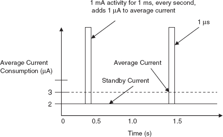
Figure 12.3 A low power design can still permit a large peak current
12.3.2 Oscillator and System Clocks
Some MCU families offer oscillator systems with up to three oscillators. These oscillators comprise the basis of their clock systems. The exact configuration is microcontroller dependent. The basic clock module (Figure 12.4) allows the optimum balance to be found between minimizing power consumption and a good performance. Usually the module is accessible by the CPU as a peripheral.
Depending on the microcontroller, the module includes two or three clock sources:
- The main oscillator clock (MOSC) is a clock source that can be synchronized with external clock sources or used with standard crystals, resonators, or low frequency watch crystals.
- The additional oscillator (ADOSC) is a high frequency clock source and can be used with standard crystals, resonators or an external clock source in the MHz range.
- The RC-type oscillator (RCOSC) is a clock source with RC-type characteristics.
The output clock signal MCLK (main system clock) of this module, which is used in the CPU, is software selectable from the input signals MOSC, ADOSC, or RCOSC. The selected input signal is divided by a software-selectable division factor.
There are fail-safe operations: if the external MOSC or ADOSC oscillators fail, operation reverts back to the internal RCOSC, where an internal resistor controls the current. During power-up or reset, the main system clock MCLK is automatically switched over to the RCOSC source. Software execution begins immediately, so that the application can configure the clock system as required.
In addition, if the MCU clock system provides multiple clock sources for the peripherals, the peripherals can operate while the CPU is in the sleep mode. For example, when an A/D conversion requires a high speed clock, the clock system can provide this high speed clock independently of the CPU clock. So, the CPU can sleep while the A/D converter is operational. The MCU power consumption depends markedly on the speed of the clocking system. Several times or several hundred times per second, applications may enter and exit various low power modes. Often, low power MCUs have ‘instant-on’ clocks that are ready for the CPU in less than 10 μs to 20 μs. Lowering the CPU clock frequency would result in less current consumption. However, because the processing time would increase, this will not result in energy consumption. On the other hand, increasing the CPU clock frequency can lead to some frequency instability. In that case, added time is required to wait for the frequency to become stable, which would also increase the overall processing time. Therefore, a fixed stable CPU clock frequency is preferred.

Figure 12.4 Oscillator and system clocks
In a PIC18FXXX MCU, four system clock periods are used for one instruction cycle. The system clock can be generated in one of eight different oscillator modes. With configuration bits in the nonvolatile memory, the oscillator mode is selected. The operating mode is determined by the value written during microcontroller programming. The oscillator modes are:
- External clock, external clock with I/O pin enable;
- Low frequency crystal, crystal/resonator;
- High speed crystal/resonator, external resistor/capacitor;
- External resistor/capacitor with I/O pin enable;
- High speed crystal/resonator with 4× frequency PLL multiplier enabled.
There is a main oscillator and an additional Timer 1 oscillator. The Timer 1 oscillator is a low frequency oscillator that is designed for operation at 32 768 kHz. The source for the microcontroller system clock can be switched from the default clock to the low frequency (Timer 1) oscillator. For specific applications, the most suitable oscillator option can be selected in a flexible way using the configuration bits. Switching the clock system from an ultra-low power standby mode to a high performance signal processing mode can be done very rapidly. In the MSP430 microcontroller of Texas Instruments (see Section 12.4.2) this takes less than 6 μs.
12.3.3 Interrupts
Interrupts can bring an MCU out of its low power mode. Therefore, the more interrupt inputs an MCU has, the more flexible it is in preventing current-wasting CPU polling and reducing power consumption. Polling wastes power because it requires excess current while waiting for an event to occur. A good low power MCU will have extensive interrupt capability, providing interrupts for all its peripherals, with external interrupt inputs for external events.
12.3.4 Peripherals
Peripheral power consumption and power management should also be considered when choosing a low power MCU. Some low power MCUs have an old architecture that was not designed for low power. Nowadays, some MCUs have the capabilities to divide the CPU clock and to clock the peripherals with this divided clock, which reduces power consumption.
12.3.5 Summary
Choosing a low power MCU or DSP requires investigation beyond data-sheet bullet points. This effort pays off because it can easily extend battery lifetime, help to meet the current budget, or keep the self-heating of smart sensor systems below certain limits.
12.4 Timer Modules
Timer modules are designed for the measurement of time intervals between 0–1 and 1–0 transitions of input signals or, in case of periodic signals, frequencies and period times.
12.4.1 Introduction to Timer Modules
Time measurements
Several principles can be applied to the measurement of time intervals or frequencies, namely:
(a) By means of permanent software monitoring (polling) of the input signal level and by incrementing the value in a software counter;
(b) By means of permanent software monitoring (polling) of the input signal level and by subsequent reading of the value of a general-purpose embedded counter (hardware counter) in the microcontroller;
(c) By using a microcontroller input with an option to interrupt servicing during change in the input signal level (interrupt input) and subsequent reading of the value of a general-purpose hardware counter;
(d) Using a hardware mechanism (input capture) capable of automatically copying the content of its respective hardware free-running counter into a register;
(e) In similar ways, frequency measurements can be accomplished by counting the number of threshold-crossings at an input per unit of time.
(a) Measurement by means of permanent software monitoring (polling) of the input signal level and by incrementing the software-counter value is the most common method, which can be applied by all microcontrollers irrespective of their structure, software type, and embedded peripheral modules. However, polling takes up the entire resources of the processor and prevents the execution of any other task. In this case, the conversion time will be the time needed to execute the basic cycle of input signal reading, to determine its level and, when this level is unchanged, to increment the value of the software counter by one unit. For this reason, the accuracy is a function of several variables, namely: the processor system clock, the number of system-clock periods needed to execute commands, the availability of efficient instructions for reading the input signal, the number of bits of the preset counter, and the availability of efficient commands for incrementing the counter value.
(b) Measurement by means of permanent software monitoring (polling) of the input-signal level and by subsequent reading of the value of the general-purpose hardware counter can be accomplished with microcontrollers with a hardware-counter module. It also takes up the entire resources of the processor and again prevents the execution of any other task. In this case, the conversion time is the time needed to increment the hardware counter. The basic cycle consists of input signal reading, setting its level and, when the latter changes, reading the hardware counter value. The lack of need to increment the counter in the basic cycle naturally leads to less conversion time and greater accuracy than in the case of applying a software counter. The accuracy is a function of the system clock of the processor, the number of system clock periods needed to execute the commands, and the availability of effective commands for reading the input signal. When the number of bits of the hardware counter is insufficient, expansion with a software counter is necessary, which will further diminish accuracy.
(c) Using a microcontroller with an embedded hardware counter and interrupt capabilities. In that case, during a level change of the input signal (connected to an interrupt input), the value of its embedded hardware counter is read. In such cases, during the time interval in between the changes in input-signal level, the processor will be idle so that it can perform other tasks. In this case, the conversion time equals the time needed to increment the counter. The accuracy is determined by the time needed to process the interrupts by the processor. When the number of bits of the hardware counter is insufficient, it should be programmed to be expandable with a software counter.
(d) Using a microcontroller with an embedded hardware mechanism. These modules (Figure 12.5), which are sometimes called input capture modules, are capable of automatically copying the content of its free-running counter into a special register. In this case, the conversion time is the time needed to increment the hardware counter. Hence, accuracy, is not determined by the time needed to process the interrupt request to the processor, but is restricted only by the conversion time. When the number of timer bits is insufficient, it should be programmed to be expandable with a software counter.
(e) In some sensor applications, instead of time intervals, the frequency of periodic signals has to be measured. When the signal is relatively high, this can be performed by counting the number of pulses sent to the input per unit of time. The conversion error is directly related to the number of pulses. Therefore, for low frequency signals, this method will require a relatively (very) long measurement time to obtain a certain accuracy. For this reason, it is more practical to use a microcontroller-embedded hardware counter with an external input to count the incoming pulses. Measurement time can be set with the help of software delay or by generating an interrupt request from the timer system, if present.

Figure 12.5 Time interval measurement using a hardware mechanism (input capture module)
Generation of pulse-width-modulated signals
Using principles similar to those used for time interval measurements, digital pulse-width-modulated (PWM) signals can be generated in the following ways:
(a) Using software settings and a software counter;
(b) Using software settings and a general-purpose embedded hardware counter;
(c) Using a microcontroller-embedded peripheral module called the output-compare module;
(d) Using a microcontroller-embedded peripheral module called the PWM module.
Some details of these methods will be discussed now.
(a) A common method of signal generation is to use software settings for determining the desired logical status of the respective output pins/ports and for determining the delays between changes of the logical levels. This method can be applied to all microcontrollers, irrespective of their structure, software type, or embedded peripheral modules. However, this method also has many drawbacks, such as:
- Applying this method takes up a significant part of the resources of the processor, which hinders the implementation of other tasks.
- During two consecutive changes in the logical status of the generated signal, the execution of any other tasks requires accurate setting of their time duration, because these will directly contribute to the length of the time intervals. This forms an obstacle to the implementation of conditional branching in the software algorithm, because the individual branches must be of the same duration.
- The conversion time will depend on the time needed for the microcontroller to execute commands. Consequently, the accuracy will be a function of the processor-clock frequency, the number of clock intervals needed to execute the commands, and the availability of certain commands to set a given output at logical zero or unit.
- Programming with a high level language, such as C, is not possible, because the time needed to execute software procedures depends on the specific implementation by the compiler, which is often inaccessible for the programmer. Therefore, using a software timer requires low level programming (Assembler).
(b) The use of a microcontroller with a microcontroller-embedded hardware counter will solve the problems mentioned for the previous method. Similar to the previous method, software settings are used to determine the desired logical status of the respective output pins/ports. Two basic varieties of this method can be found:
(1) Permanent software polling of the value of the hardware counter. When a pre-set value is reached, certain outputs will be set in pre-set states. With this method, the signal generation takes up the entire resource of the processor and makes it difficult to execute any other task. The conversion time depends on the frequency by which the value of the hardware counter is incremented. Furthermore, the time-interval resolution is limited by the time needed to read the counter-value, to compare that value with the preset limit, and potentially to change the output level.
(2) The output-level change is only done at an interrupt caused by a hardware-counter overflow. Usually, this is done after a certain number of overflows. This method takes up a significantly smaller part of the microcontroller resources. However, the resolution of the generated time intervals is significantly larger than in the first case, because it depends on the counter-overflow time (with 8-bit counters it is 256 times larger than in the first case). The accuracy depends on the time needed to process the interrupt call by the microprocessor and the time needed to set the output to the respective logical status. However, the accuracy is much more precise than when not set at that time, and will depend on the moment of generation of the interrupt call compared with the rest of the program.
(c) Another method of signal generation is to use a microcontroller-embedded peripheral module, called an output-compare module (Figure 12.6). When the value of a register, which is specially designated for this purpose, coincides with that of a microcontroller-embedded counter, this module sets a given output into a logical-unit or logical-zero state. In this case, the resolution of the time intervals equals the time needed to increment the counter value. The accuracy depends only on the system-clock phase in which the microcontroller checks and sets the output.
The minimum duration of the generated pulse is limited by the time needed for the microcontroller to compute and set the new value of the output compare register and eventually to change the output signal. In the case that periodic output signals are generated, simplification of the method is possible, especially when the microcontroller has the option of using two or more output functions of the individual output compare registers, while using one and the same counter. In that case, the minimal duration of the generated pulse will be equal to the time duration needed to increment the counter, which corresponds to one timer-clock period. When using counter overflows, there is a hardware option to generate periodic signals with a frequency equal to the frequency of the counter overflows, or to divide this frequency with an integer overflow factor.

Figure 12.6 Signal generation using a microcontroller-embedded output-compare module
(d) Signal generation using a microcontroller-embedded PWM module is capable of generating its own periodic signal after setting the duration of the logical zero and setting the logical unit in a register specially designated for the purpose. The availability of such a module makes it easy to program periodic signals. Moreover, the generation of these signals does not consume much of the microprocessor resources. This implementation can be regarded as a perfection of the method for periodic-signal generation discussed above in (c). The minimal duration of a generated pulse equals the time needed to increment the counter (one clock period).
12.4.2 Examples of Timer Module Applications for Various Microcontrollers
The MSP430 family of Texas Instruments
The microcontrollers of the MSP430 family have a 16-bit RISC mixed-signal processor. They are equipped with powerful capabilities that make them attractive for applications in smart sensor systems. For instance, there are features for both analog and digital signal processing. Moreover, in less than 6 μs, the clock system can switch from an ultra-low power standby mode to a high performance signal-processing mode. The main features of the MSP430 microcontrollers are:
- Ultra-low power architecture;
- Modern 16-bit CPU–RISC architecture;
- 8 MIPS;
- High performance analog part – ideal for measurements;
- In-system programmable flash memory – easy for changes;
- Embedded emulation, which reduces design cycle time;
- Modular design concept and memory-mapped peripherals;
- All registers are included in modules;
- Easy program development due to the orthogonal structure;
- All instructions can be used for all-addressing modes.
With its high level of analog integration and its low power consumption, the MSP430 can provide complete solutions for embedded applications, including smart sensor systems.
The MSP430 has a general-purpose 16-bit timer, Timer A, with the following features:
- A 16-bit counter with four operating modes;
- Selectable and configurable clock sources;
- Three or five independently configurable capture/compare registers with configurable inputs;
- Three or five individually configurable output modules with eight output modes.
The Timer A scheme is shown in Figure 12.7 (pins (Px.x) are for MSP430F1121).
Timer A can work with either selected inputs, functions as capture/compare, or with the function to output various waveforms, such as PWM signals. Furthermore, any additional capture/compare register has hardware support for implementing serial communication according to, for instance, a UART protocol. The interrupt properties of Timer A can be used to generate interrupts from the counter upon overflow conditions and from each of the capture/ compare registers on captures or compares. Each capture/compare block is individually configurable and can produce interrupts to detect rising edges, falling edges, or both, of an external capture signal.
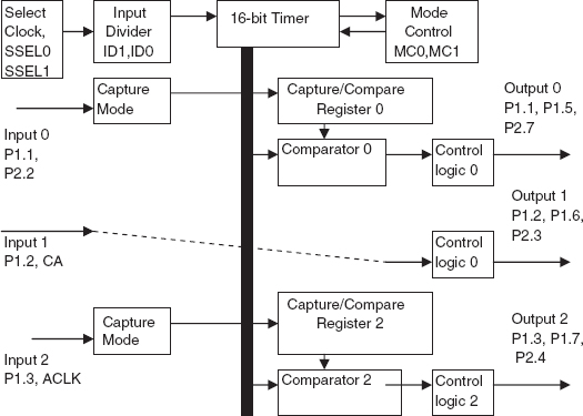
Figure 12.7 The MSP430 general-purpose 16-bit timer, Timer A
The four modes of operation are selectable with the mode-control bits MC0 and MC1 in a special register. These modes are called: stop mode, up mode, continuous mode, and up/down mode. Depending on the mode of operation, the timer increases or decreases incrementally with each rising edge of the clock signal. The timer can be read or written according to the program. The clock source is selectable with the SSEL0 and SSEL1 bits in a special register. Changing the clock source can cause a timing error. Therefore, it is recommended to stop the timer before changing the clock source. The clock division factor can be selected with the ID0 and ID1 bits in a special register. The capture/compare blocks provide flexible control for real-time processing and can be used to capture the timer data at an applied event, or to generate time intervals. Interrupts can be generated from the registers each time a capture event occurs or a time interval is completed.
Example 12.1: Measuring UTI signals with Timer A. The universal transducer interface (UTI) (see Chapter 2, Section 2.6) has a period-modulated output signal. Figure 12.8 shows how the UTI is connected to the MSP430. The period times can be measured by using the capture mode for time measurement, using the capture/compare block of timer A. The input signal of the capture/compare block is selected using the CCISx1 and CCISx0 control bits. The timer value is copied into the capture register with the selected edge (positive, negative, or both) of the input signal.

Figure 12.8 Measurement using Timer A and UTI
From the measured time intervals, the MSP430 microcontroller can calculate the sensor input signal from the UTI, and perform further calculations and do data processing. The calculated result is sent via the MAX232 to some of the COM ports of a PC.
The PIC18 of Microchip
These microchips concern a family of CMOS, fully static, 16-bit MCUs with RISC CPU architecture. The high performance of the PIC18 microcontrollers is a result of features commonly found in MCUs with RISC architecture. The Harvard architecture with its separate instruction and data bases, allows the use of 16-bit-wide instruction words together with separate 8-bit-wide data. The two-stage instruction pipeline allows all instructions to be executed in a single cycle, except for program branches, which require two cycles. The PIC18, with the highest level of analog integration and low power consumption, provides complete solutions for embedded applications as part of smart sensor systems, portable instrumentation, and gas, water, and electricity meters. Most of the PIC18 microcontrollers provide flash-programmable memory in sizes ranging from 8 to 128 kBytes and data RAM from 256 Bytes to 4 kBytes. The speed is from dc to 40 MHz and the required supply voltage ranges from 2.0 V to 5.5 V. Optimized for high level programming languages, such as ANSI C, the PIC18 family provides a flexible solution for complex applications.
The peripheral features include:
- Up to three 16-bit timer/counters;
- Up to two 8-bit timer/counters with 8-bit period register (for PWM);
- Up to four external interrupt pins;
- a secondary low power oscillator, using Timer 1;
- Up to five capture/compare/PWM (CCP) modules;
- A master synchronous serial port (MSSP) module;
- Up to 2 addressable USART modules;
- One parallel slave port (PSP) module;
- 10-bit analog-to-digital converters (ADCs).
Power management features are:
- Dynamic switchover to secondary low power oscillator;
- Internal RC oscillator for ADC performance;
- Sleep mode;
- Internal RC oscillator for the watch-dog timer WDT;
- RAM retention mode.
For some of the PIC18 microcontrollers more than six selectable power-management modes are available.
Each CCP module contains a 16-bit register which operates as a 16-bit capture register, as a 16-bit compare register, or as a PWM master/slave duty-cycle register. The module CCP1 is used to describe the operation of the CCP module as applied, for instance in the capture mode, which is used for time interval measurements. The CCPx can be coupled to Timer 1 or Timer 3 to measure time intervals between signal edges occurring at the CCPxPin. The input signal can be divided by a prescaler or the prescaler can be bypassed to set the CCPxIF bit. The CCPxIF can be set at edge detection (falling or rising) of the input signal.
Example 12.2: Measurement of the output signal of a smart temperature sensor with a PIC18 microcontroller. The SMT160-30 is a smart temperature sensor, which has been described in Chapter 7, Section 7.5. Figure 12.9 shows how this sensor can be connected to a PIC18 microcontroller.
Figure 12.9 Setup of a temperature measurement system with a PIC18 microcontroller timer and an SMT160-30 smart temperature sensor
The output signal (Figure 12.10) of the SMT160 (www.smartec.nl) is a duty-cycle-modulated square wave with a well-defined temperature dependence. The duty cycle M(T) = t1/(t1 + t2) of the output signal is linearly related to the temperature, according to the equation:

Figure 12.10 A duty-cycle-modulated signal
where θ is the temperature in °C and the duty cycle M(T) varies from 0 to 1. The most efficient way to measure the duty-cycle values is to use the input capture capability of the microcontroller. The 16-bit timer Timer 1 should be configured in the timer mode for the highest possible counting frequency (10 MHz), which gives a resolution of 100 ns. In order to measure the time-interval duration, the user application should ‘capture’ consecutive rising/falling edges of the input signal and subtract the rising-edge Timer 1 value from the falling-edge value. First ‘capturing’ and then subtracting the Timer 1 values of two consecutive rising edges is used to measure the period. To reduce the quantization error, different digital filtering techniques can be used. For example, averaging multiple results over a number of periods will increase the system precision by a square root of that number (see Chapter 10).
The LPC2000 family of NXP
The LPC2000 microcontrollers are based on a 32/16-bit ARM7TDMI-S CPU with a 128-bit memory interface and unique accelerator architecture which enables 32-bit code execution at the maximum clock rate. The sizes of the embedded high speed flash memories range from 8 kB to 512 kB. The ARM7 is a RISC computer with a small instruction set, which makes it ideal for embedded systems, including smart sensor systems. On the ARM7 a three-stage pipeline is used with three stages: fetch, decode, and execute. This pipeline has hardware-independent stages that execute one instruction while decoding a second and fetching a third one. A set of 16 user registers, R0–R15, is available. The registers R0–R12 do not have any specific function, while the registers R13–R15 have special functions in the CPU: to register R13 as the stack pointer, R14 as the link register and R15 as the program counter. The ARM7 is implemented with a 32-bit processor. It has a second 16-bit instruction set which is called THUMB. In fact, THUMB is a compressed form of the first instruction set. By compiling the program code in the THUMB instruction set, 30 % of the required memory space can be saved. As an example of LPC2000 family members, we will consider the LPC2148, which offers:
- Flash memory up to 512 kB;
- 40 kB on-chip static RAM;
- In-system/in-application programming (ISP/IAP) via on-chip boot-loader software.
A single flash sector can be erased in 400 ms, while the programming of 256 bytes takes only 1 ms. The serial communication interfaces include a USB 2.0 full speed device, UARTS, SPI, SSP, and I2C. Furthermore, there are various 32-bit timers, dual 10-bit ADCs, a 10-bit DAC, PWM channels, and 45 fast GPIO lines with nine edge- or level-sensitive external interrupt pins. These features make these microcontrollers highly suitable for smart sensor system applications. More information can be found in the LPC2148 User Manual and Data sheet (www.nxp.com).
Now, some examples will now be given to show how to use the LPC2148 with different types of sensors. In addition, some C programs will show how to read from transponders, how to calibrate sensor systems, and how to perform digital information processing, such as averaging or linearization.
Example 12.3: Radio frequency identification (RFID). Figure 12.11 shows a circuit diagram of a RFID system. Such systems are applied in electronic tags or transponders used for identification purposes. The Melexis(4) MLX90109 is a single-chip RFID transceiver for the 125 kHz range. It can be used to read out the load modulation of a transponder. An external coil (L1) and a capacitor (C1) are connected as a parallel resonant circuit and determine the carrier frequency and oscillator frequency of the reader. The presented circuit provides control signals for MLX90109 to set, for instance, the speed and the mode, to set the antenna voltage to the required level via the input MODU, to read data, and to set the clock.
Figure 12.11 RFID with the Melexis MLX90109. The port pins are connected to an LPC2148 microcontroller
The circuit depicted uses the general-purpose digital input/output (GPIO) pins P0.2, P0.4, P0.5, P0.6, and P0.7 of the LPC2148 microcontroller and enables the MLX90109 to read data, to write with a speed of 2 kbaud/4 kbaud, and to select the encoding mode Biphase or Manchester. Figure 12.12 presents a program, written in C language. This program is used to read the contents of the transponder (128 bits) and to send them, via the serial interface, to a PC. On the PC, the standard program ‘hyper terminal’ is activated for data receiving and visualization. The source code begins with the initialization of the MLX90109, the serial port, and the peripherals of the microcontroller. Data and clock lines of the MLX90109 are connected to the GPIO pins P0.7 and P0.2 of the microcontroller. Pin P0.2 is initialized to receive interrupts on the rising edge of the signal. Using the interrupt service routine, the level of pin P0.7 is checked. The value of the recognized data ‘0’ or ‘1’ is stored in the array valu[I], which has the size of 250 elements. After storing the 250 values, the algorithm starts with header (synchroword ‘00000000001’) searching. After finding the synchroword, 128 bits with values ‘1’ or ‘0’ are transmitted via the serial interface. If data recognition is necessary, an additional code must be added to the source code.

Figure 12.12 The C program for RFID identification with TIMERO of an LPC2148 and the Melexis transceiver chip MLX90109
Example 12.4: Measuring duty-cycle modulated signals with an LPC2103 timer and a smart temperature sensor. Figure 12.13 shows a block diagram of a temperature measurement system with an LPC2103, a smart temperature sensor SMT160 (see Chapter 7, Section 7.5) and a RS232 interface circuit. The power supply voltage of the sensor is 5 V and the sensor output voltage is 0 V to 5 V. This level is acceptable for the LPC2000 inputs. The sensor SMT160-30 is connected to input terminal P0.2 of the microcontroller. The temperature data are transmitted to a PC, via the serial interfaces UART1 of the microcontroller and a MAX232. After initialization, at every interrupt event the program (Figure 12.14) reads the value of the counter. The interrupts are generated on the rising and falling edges of the input pin P0.2. Because of the high frequency (70 MHz) of the timer, the sampling error is an order of magnitude less than when, for instance, a PIC18 microcontroller would have been used. Therefore, a high measurement precision can be achieved (see Chapter 10, Section 10.3.4). In the array VALU [I] which has the size of 22 elements, the sequence of the width of ‘1’ and ‘0’ time intervals of the SMT160-30 output voltage is consecutively recorded.

Figure 12.13 Block diagram of a measurement system with an LPC2103 timer and an SMT160-30 smart temperature sensor
The program is organized so that the recording starts with a ‘1’ time interval. When the array is full, the data are processed by summing ten values of the ‘1’ time intervals and ten values of the full period. In this way, the average of ten measured values is achieved. The program continues with computing the temperature, according to Equation (12.1), and transmitting the final result via UART1 to a PC for visualization.

Figure 12.14 This C program shows how to use the TIMER0 of a LPC2103 microcontroller for measuring of the duty-cycle-modulated output signals of an SMT160-30 smart temperature sensor
Example 12.5: Measuring period-modulated signals of universal sensor interfaces with an LPC2103 timer. Figure 12.15. shows how to connect the universal sensor interface UTI (see Chapters 2 and 10) to the LPC2136 microcontroller. The setup displayed is valid for a UTI in mode 5 (Pt100, four-wire). The program (Figure 12.16) begins with initialization, which determines the interrupt request on the rising edge of the input signal and an array VALU [I] with 22 elements which is reserved for the values. When the records in the array have been completed, the period values are computed and the results are stored in a new array: period [I]. The next step is to search the minimum value of the period and compute the value of the Pt100 sensor.
Figure 12.15 The connection of a universal sensor interface UTI to an LPC2136 microcontroller for temperature measurements with a Pt100


Figure 12.16 This C program shows how to use TIMER0 and UTI to measure periods and calculate the values of a Pt resistor
The TMS320LF240xA DSP of Texas Instruments
The members of this family of 16-bit DSP controllers are equipped with a CPU with RISC architecture. They are designed to meet a wide range of digital industrial control applications. The DSPs have a 16-bit, fixed-point, low power CPU, and are complemented with on-chip peripherals and on-chip ROM or flash program memory in addition to an on-chip dual-access RAM. The TMS320 DSPs have an architecture designed especially for real-time signal processing. The controller peripherals are highly suited for control-system applications. The following characteristics make the TMS320 family an excellent choice for a wide range of processing applications: flexible instruction set, inherent operational flexibility, high speed performance, parallel architecture, and cost effectiveness. The 240xA DSP controllers are implemented as customizable digital processors.
Event managers
The timer modules in the DSPs are called event managers (EVs). The EV module provides different functions and features that are particularly useful in motion control and motor-control applications, as well as in all types of inverters. All members of the 240xA family, with the exception of the 2402A, have two event managers, EVA and EVB. These two event managers are identical in terms of functionality and registering mapping definitions. Each EV module contains the following functional blocks:
- Two general-purpose timers;
- Three compare units;
- PWM circuits that includes a space vector PWM circuit, a dead-band generation unit, and output logic;
Figure 12.17 QEP circuit of an event manager module
- Three capture units;
- A quadrature encoder pulse (QEP) circuit;
- Interrupt logic.

The general purpose timers can be used as independent time bases in applications such as:
- Generation of a sampling period in a control system;
- Providing a time base for the operation of QEP circuits and capture units;
- Providing a time base for the operation of the compare units and the associated PWM circuits which generate PWM outputs.
QEP circuit
Each event manager module has a QEP circuit. The QEP circuit decodes and counts the quadrature encoder input pulses at the corresponding pins. This circuit can be used to interface an optical encoder as a sensor as well as to obtain position/speed information from a rotating machine. Figure 12.17 shows the block diagram of a QEP circuit, and Figure 12.18 shows the timing diagram of the main signals.
QEPs are arranged into two sequences, with a variable frequency and a fixed phase shift of a quarter of a period (90°). When generated by an optical encoder on a motor shaft, the direction of rotation of the motor can be determined by detecting the phase shift of the two sequences. The angular position and speed can be determined by the pulse count and the frequency.

Figure 12.18 The timing of signals
12.5 Analog Comparators, ADCs, and DACs as Modules of Microcontrollers
12.5.1 Introduction
The microcontroller developments have brought along the integration of analog and digital modules on chip, which has resulted in so-called mixed-signal systems that include analog and digital parts on the same piece of silicon. The use of mixed-signal microcontrollers requires some specific measurement technique to be used in order to improve the noise immunity of the system.
There are not many microcontrollers with built-in operational amplifiers. However, many microcontrollers contain built-in analog-comparator modules. The presence of on-chip analog comparators gives the opportunity to monitor the threshold of the power supply or the level of external analog signals. Usually, there is also a built-in programmable voltage source for setting the threshold level. In some microcontrollers, the analog comparator module is designed to facilitate specific applications, such as the arrangement in a sigma-delta analog-to-digital conversion.
Analog-to-digital converters (ADCs) nowadays form an irrevocable part of a microcontroller. In the very beginning, most integrated ADC modules were of the 8-bit type, which was not sufficient for many applications. In more recent generations of microcontrollers, 10- and 12-bit ADCs are also used. There are also microcontrollers with built-in 16- and even 24-bit ADCs. Often, the conversion time of built-in 24-bit ADCs exceeds 100 ms, while built-in 10- to 12-bit ADCs have conversion times between 5 and 20 μs. In most cases, the ADCs make up part of a multi-channel system with a dedicated register block for control and with data storage.
There are also microcontrollers with built-in digital-to-analog converters (DACs). This makes it possible to obtain a pure analog-output signal. In most cases, there are 12-bit DACs with at least two independent channels. The presence of DACs in the system can also give some advantages during the design and testing stage. The use of DACs enables real-time monitoring of, for instance, high frequency variables with a low frequency oscilloscope.
12.5.2 Application Examples of Analog Modules
MSP430 Comparator A
Comparator A of a MSP430 microcontroller is used as a peripheral module to compare analog signals. The Comparator A module includes: a comparator with on/off capability, an internal voltage reference, an input multiplexer to exchange the comparator terminals, a software-selectable RC filter at the comparator output, and one interrupt vector.
The main function of the Comparator A module is its use for analog-to-digital slope conversion and monitoring of external analog signals. Comparator A is controlled via 12 control bits in internal registers. Two 8-bit registers are used to configure the comparator. The CAON (Comparator A ON) bit enables power supply to reach the comparator. The (+) and (−) inputs of the comparator can be connected to either an external pin or an internal reference voltage. The CARSEL bit applies an internal voltage to one of the comparator connections. These intermediate connections are routed to the comparator inputs by the CAEX bit. Swapping an input bit inverts the sign of the comparator output. An internal reference voltage is selected via the CAREF bits. There are four reference-voltage sources that can be selected.
Example 12.6: Measurement options with the Comparator A Module. The Comparator A Module can be used to compare input signals and to measure voltage, current, capacitance, and resistance. The hardware configuration in Figure 12.19 shows the principle for measuring a resistive sensor Rsens. In the scheme of Figure 12.19, the only external components needed are the sensor resistor Rsens, a reference resistor Rref, and a capacitor Cm. Before each measurement, the capacitor Cm is charged with the voltage Vcc. At the start of the capacitor discharge, the contents of the TAR timer register (which in continuation mode always counts upwards) are stored. When the voltage over capacitor Cm reaches the threshold value of 0.25Vcc, the negative edge of CAOUT causes the actual TAR value to be captured in CCR1 register. The difference between the CCR1 value and the start value represents the discharge time interval tsens or tref, respectively. Figure 12.19 shows the Vcm voltage across the capacitor Cm during the measurement of Rref and Rsens, respectively. The charge time tc must be between 5RrefCm and 7RrefCm, depending on the accuracy required.

Figure 12.19 Setup for the Comparator A Module
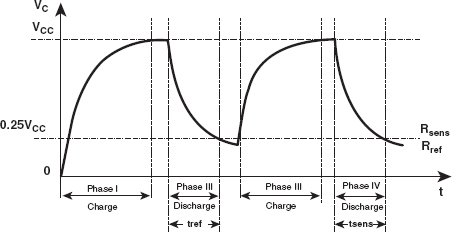
Figure 12.20 The voltage Vcm across capacitor Cm during two measurements
For nonlinear sensors (such as NTC sensors), a shunting resistor Rshunt is connected in parallel to the sensor resistor. Its value is chosen for optimum linearity (see Chapter 7, Section 7.3.2). The final result can be calculated as:
Measurement using the ADuC834(5) of Analog Devices
To reduce the complexity of sensor systems, a microcontroller with a built-in ADC, such as the ADuC834, can be used. The features of these so-called microconverters are:
- Two independent ADCs (16-bit and 24-bit resolution);
- One memory (62 kBytes program flash, 4 kBytes data flash, 2 kBytes data RAM);
- An 8052-based core;
- A programmable PLL (12.58 MHz max);
- Three 16-bit timers/counters;
- An internal power reset circuit;
- A 12-bit DAC;
- Dual 16-bit DACs as PWMs;
- An on-chip temperature sensor;
- Dual current sources;
- A UART;
- An SPI interface;
- An I2C interface;
- Watchdog timer WDT;
- Power supply monitor.
The ADuC834 has self-calibration features to calibrate offset and gain errors. The ADuC834 is suitable for intelligent sensors, portable instrumentation, and precision system monitoring. The ADuC834 has two independent ADCs (primary and auxiliary). It includes a temperature sensor and a programmable gain amplifier (PGA) which permit direct measurement of low level signals. The on-chip digital filtering and programmable output-data rates are intended for measuring wide dynamic-range, low frequency signals. The microcontroller operates from a 32 kHz crystal with an on-chip PLL, which generates a high frequency clock up to 12.58 MHz. The core is 8052 compliant and therefore the instruction set is compatible with an 8051 core. The on-chip firmware maintain in-circuit serial download using debug modes (via the UART), or by using a single-pin emulation mode via a special pin.
Example 12.7: Temperature measurement with an RTD Pt100. Figure 12.21 shows a setup for measuring temperature with an RTD Pt100 (see also Chapter 7, Section 7.3). For precision purposes the ratiometric approach has been chosen. For this, a resistor Rref is connected in series with the RTD. The resistor generates a reference voltage that is fed directly to the ADC. Fluctuations in the current can be neglected, because these cause proportional voltage drops over both the reference resistor and the RTD. In order to use this approach, the user needs a fully differentiated input and reference ADC, such as the one used for the ADuC834.

Figure 12.21 An RTD Pt100 temperature measurement with the ADuC834
12.6 Embedded Networks and LCD Interfacing
System-on-chip (SoC) solutions require different interfacing modules. For this purpose, some MCU and DSP devices also include different types of interface modules.
One of the most widespread interfaces is the universal synchronous/asynchronous receive/ transmit (USART) module. Often, in MCU and DSP devices, one or two USART modules have been built in. The universal reception/transmission (USART) serial-communication peripheral has two serial modes: a synchronous and an asynchronous one. The asynchronous mode is more popular and shifts a serial stream of bits into and out of an MCU or DSP, at a programmed rate defined by a clock. It uses a standard non-return-to-zero (NRZ) format: one starting bit, eight or nine data bits, and a stop bit. An on-chip baud-rate generator delivers signals with standard baud-rate frequencies. Usually, the users have to provide external level-shifted buffers to translate the RS232 levels to the logical levels used by the MCU or DSP.
The serial peripheral interface (SPI) is the most common synchronous data-transmission module, which uses data and clock signals to transmit and receive serial data. The master supplies the clock and the data. The slave uses this clock to shift serial information in and out. The SPI is primarily used to allow the MCU or DSP to communicate with peripheral devices. The SPI is also capable of interface communication in a multiprocessor system. This interface is flexible enough to act directly with numerous standard product peripherals. Usually, the system can be configured as a master or a slave device.
The availability of a liquid crystal display (LCD) controller gives the possibility of direct driving of the LCD displays by automatic generation of the ac voltages for the segments and common. The LCD controller features are: display memory, automatic signal generation, configurable frame frequency, blinking capability, and support for different types of LCDs.
The controller area network (CAN) driver uses a serial multimaster communication protocol that efficiently maintains distributed real-time control with a very high level of data reliability. A CAN bus is ideal for applications in noisy environments, such as in the automotive and other industrial fields which require reliable communication.
12.7 Development Tools and Support
Hardware and software development tools facilitate design of MCU and DSP systems. Without such tools, it would be very difficult to develop, test, and use MCU and DSP systems. Usually, MCU and DSP manufacturers offer a wide range of hardware and software development tools which are designed in the company or by third-party companies. For first users there are the so-called starter kits, or evaluation modules. Those systems facilitate the introduction of specific features of a single MSUs or DSPs. They have the possibility of program loading, memory writing, debugging, etc. Usually in modern microcontrollers this is done by JTAG or some other in-circuit debugging interface. Such a simple tool also has the possibility of programming on board using its flash memory. There are also more complex hardware development tools, such as in-circuit emulators, which give the opportunity for full real-time debugging.
Usually, software development is carried out in an integrated development environment (IDE) running on a personal computer. In the IDE all the necessary compilers and linkers are included so that Assembly as well as the C languages can be used. With a standard hardware tool, the program can directly be loaded in the microcontroller. Usually, a software simulator is also available.
Many companies offer various real-time operation systems (RTOS) and an enormous amount of libraries for specific applications. For some microcontrollers, graphically oriented programming languages are also available.
12.8 Conclusions
Significant advancements of MCUs and DSPs regarding performance, price, and integrated features, have ensured that digital control is preferably performed on chip. The availability of analog-to-digital and digital-to-analog converters provides very powerful solutions for most smart sensor system design problems.
The low power consumption of MCUs facilitates their use in portable instrumentation.
Continuously increasing amounts of MIPS and converter accuracy contributes to improved resolution and reliability of smart sensor systems. Even in the most cost-sensitive products MCUs and DSPs are increasingly embedded. For smart sensor systems, these devices are indispensable,
Reference Sites
Smart Sensor Systems Edited by Gerard C.M. Meijer
© 2008 John Wiley & Sons, Ltd