LEDs are small, rugged, and bright light sources with a huge potential to become the dominant light source in the future. Nowadays, LEDs are the most efficient sources of colored light in the visible range of the spectrum. White LEDs already surpassed incandescent lamps in performance and undergo continuous improvement of their efficiency. Today, almost a quarter of the electric energy used is spend for lighting, and perhaps half of this energy could be saved by the employment of efficient and cold solid-state lighting sources [5]. It seems that “Optopia” is on its way and solid-state light sources are at the forefront of the ongoing lighting revolution.
At present, commercially available LEDs cover the spectrum from near-UV through visible to near-IR regions. Apart from the lighting industry, LEDs find numerous applications in automotive and aviation industry, in large area displays and communication systems, in medicine and agriculture, in amusement media industry, and other in everyday life consumer products.
A considerable amount of books and publications is dedicated to the fundamentals, technology, and physics of LEDs, their electrical and optical properties, and advanced device structures (e.g., see Refs. [9,10,11,12,23,26], and the references thereafter). We give here only a brief summary of the LED characteristics relevant to optical metrology and some applications.
LEDs are semiconductor devices, which generate light on the base of electroluminescence due to carrier injection into a p−n junction. Basically speaking, an LED works as a common semiconductor diode: the application of a forwardly directed bias drives a current across the p−n junction. The excess electron–hole pairs are forced by the external electric field to enter the depletion region at the junction interface where recombination takes place. The recombination process can be either a spontaneous radiative process or a non-radiative process with energy release to the lattice of the material in the form of vibrations (called phonons). This dual process of creation of excess carriers and subsequent radiative recombination of the injected carriers is called injection electroluminescence. LEDs emit fairly monochromatic but incoherent light owing to the statistical nature of spontaneous emission based on electron–hole recombinations.
The energy of the emitted photon and the wavelength of the LED light, depends on the band-gap energy of the semiconductor materials forming the p−n junction. The energy of the emitted photon is approximately determined by the following expression:
where
h is the Planck’s constant
ν is the frequency of the emitted light
Eg is the gap energy, that is, the energy difference between the conduction band and the valence band of the semiconductor used
The average kinetic energy of electrons and holes according to the Boltzmann distribution is the thermal energy kT. When kT ≪ Eg, the emitted photon energy is approximately equal to Eg, as shown by Equation 1.41, whereas wavelength of the emitted light is
where c is the speed of light in vacuum. For example, Eg of GaAs at room temperature is 1.42 eV and the corresponding wavelength is 870 nm. Thus, the emission of a GaAs LED is in the near-IR region. It is known from the literature [12,87,88] that the emission intensity of an LED is determined by the values of Eg and kT. In fact, the intensity I(E) as a function of photon energy E is given by the following simple expression:
The maximum intensity of the theoretical emission spectrum of an LED given by Equation 1.43 occurs at energy
and the full width at half maximum (FWHM) of the spectral emission corresponds to
For detailed derivation of these expressions, see Section 5.2 in Ref. [12].
In general, the spectral power distribution of an LED tends to be Gaussian with a specific peak wavelength and a FWHM of a couple of tens of nanometers. At room temperature, T = 293 K, kT = 25.3 meV, and Equation 1.45 gives the theoretical FWHM of an only thermally broadened emission band of an LED, ΔE = 46 meV. The FWHM expressed in wavelength, Δλ, is defined by
For example, the theoretical spectral linewidth at room temperature of a GaAs LED emitting at λ= 870 nm is Δλ= 28 nm. The output spectrum depends not only on the semiconductor band-gap energy but also on the dopant concentration levels of the p−n junction. Random fluctuations of the chemical composition of the active material additionally broaden the spectral line (alloy broadening). Therefore, realistically, the emission broadening ΔE of LEDs is between 2.5 and 3kT. A typical output spectrum of a red GaAsP LED (655 nm) has a linewidth of 24 nm, which corresponds to an energy spectrum of about 2.7kT of the emitted photons at room temperature [88]. Nevertheless, despite the broadening, the typical emission spectrum of an LED is fairly narrow and appears to be monochromatic to the human eye.
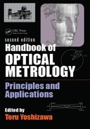
The peak wavelength of an LED is the wavelength at the maximum intensity of the LED emission spectrum and is generally given in LED data sheets. However, the peak wavelength has little significance for practical purposes since two LEDs may have the same peak wavelength but different color perception. Therefore, the dominant wavelength, which is a measure of the color sensation produced by the LED in the human eye, should be also specified. Figure 1.16 illustrates how the dominant wavelength of an LED can be determined from the CIE color diagram: a straight line is taken through the color coordinates of a reference illuminant, generally the equal energy point E and the LED measured color coordinates F. The intersection point S of the straight line with the boundary of the color diagram gives the value of the dominant wavelength. Purity is another important colorimetric characteristic of LEDs, which is defined by the ratio of the distance E–F from the equal energy point E to the LED color coordinate F and the distance E–S from the equal energy point E to the intersection point S in the color diagram. Most LEDs are narrow-band radiators with a purity of nearly 100%, that is, the color is perceived as monochromatic light.
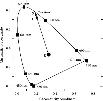
FIGURE 1.16 Dominant wavelength of an LED determined from the 1931 CIE color diagram for 2° observer. (From Schubert, E.F., Light-Emitting Diodes, Cambridge University Press, Cambridge, U.K., 2003. With permission.)
The output light intensity is determined by the current through the p−n junction. As the LED current increases, so does the injection minority carrier concentration and the rate of recombination, thus the emitted light intensity. For small currents, the LED light power depends linearly on the injection current. At high current levels, however, at strong injection of minority carriers, the recombination time depends on the injected carrier concentration and hence on the current itself, which leads to a nonlinear recombination rate with current. The turn-on voltage from which the LED current increases very steeply with voltage is typically about 1.5 V. The turn-on voltage depends on the semiconductor and generally increases with the energy bandgap Eg. For example, for a blue LED it is about 3.5–4.5 V, for a yellow LED it is about 2 V, and for a GaAs IR LED it is around 1 V.
The LED emission output is a function of the forward current and the compliance voltage. Therefore, LEDs are normally operated in a regime of a constant current. Following the LED switch-on, the temperature in the p−n junction gradually rises due to electrical power consumed by the LED chip and then stabilizes when a stable forward voltage is attained. The stabilization process can last several seconds and, in the case of white LEDs, might be influenced by the properties of the phosphor. Different types of LEDs have different temperature stabilization times.
As the heat from the p−n junction must be dissipated into the surroundings, the emission intensity of LEDs also depends on the ambient temperature. An increase in the temperature causes a decrease in the intensity of the emitted light due to non-radiative deep-level recombinations, surface recombinations, or carrier losses at interfaces of hetero-paired materials. The III–V nitride diodes have less sensitive temperature dependence than AlGaInP LEDs. As the ambient temperature increases, the required forward voltage for all the three diodes (blue, green, and red) decreases due to the decrease of the band-gap energy. Thus, if the ambient temperature rises, the entire spectral power distribution is shifted in the direction of the longer wavelengths. The shift in peak wavelength is typically about 0.1–0.3 nm/K. Therefore, current and temperature stabilizations are very important for attaining constant spectral properties.
In addition to radiometric and photometric characteristics, the description of the optical properties of an LED also includes the quantum performance of the LED determined by its internal and external quantum efficiencies and extraction efficiency.
The internal quantum efficiency of an LED is defined by the number of photons generated from a given active region (inside the semiconductor) divided by the number of injected electrons. The internal quantum efficiency can also be expressed with measurable quantities such as the optical power Φint (radiant flux) emitted from the active region and the injected current I:
where
hν is the energy of the emitted photon
Φint/(hν) gives the number of photons emitted from a given active region per second
e = 1.6022 × 10⁻¹⁹ C is the elementary charge
I/e is the number of electrons injected into the LED per second
An ideal active region would have a quantum efficiency of unity, because every injected electron would recombine with a hole through a radiative transition producing a photon. In reality, the internal quantum efficiency of an LED is determined by the competition between radiative and non-radiative recombination processes. High material quality, low defect density, and low trap concentration are prerequisites for large internal efficiency. Double heterostructures, doping of active region, doping of the confinement regions, lattice matching in double heterostructures, and displacement of the p−n junction into the cladding layer, all these are new LED designs that allow to increase the internal efficiency [89].
The extraction efficiency is determined by the escape probability of the photons generated in the active region, thus, by the number of the photons that leave the LED as emitted in the space per number of photons generated by the active region:
where Φair is the optical power emitted by the LED into free space. In an ideal LED, all photons emitted from the active region would escape in the space, and the extraction efficiency would be unity. In a real LED, there are losses of light due to reabsorption of the emitted light within the LED structure itself or light absorbed by the metallic contact surface or the effect of total internal reflection (TIR) from the parallel sides of the junction, which traps the emitted light into the junction region. Those are inherent losses due to the principal structure of an LED and are very difficult to reduce or avoid without major and costly changes in the device fabrication processes or LED geometry.
The refractive index of most semiconductors is quite high (>2.5) and the critical angle of TIR at the interface semiconductor/air is less than 20°. Only the light enclosed in the cone determined by the critical angle (escape cone) can leave the semiconductor. Even at normal incidence, the surface reflectivity is too high. For example, GaAs has an index of refraction 3.4, and the reflection losses for vertical incidence on the GaAs/air interface are about 30%. Thus, only a few percent of the light generated in the semiconductor is able to escape from a planar LED. There is a simple expression for the relation between the extraction efficiency and the refractive indices of the semiconductor ns and air nair [12]:
The problem is less significant in semiconductors with small refractive index and polymers, which have refractive indices on the order of 1.5. For comparison, the refractive indices of GaAs, GaN, and light-emitting polymers are 3.4, 2.5, and 1.5, respectively, and the extraction efficiencies are 2.2%, 4.2%, and 12.7%, respectively. If the GaAs planar LED is encapsulated in a transparent polymer, the extraction efficiency would be about a factor of 2.3 higher. Thus, the light extraction efficiency can be enhanced two to three times by dome-shaped epoxy encapsulants with a low refractive index, typically between 1.4 and 1.8. Due to the dome-shape, TIR losses do not occur at the epoxy–air interface. Besides improving the external efficiency of an LED, the encapsulant can also be used as a directing spherical lens for the emitted light.
The photon escape problem is essential especially for high-efficiency LEDs. To achieve an efficient photon drag out of LEDs is one of the main technological challenges. The extraction efficiency optimization is based on modifications and improvement of the device geometry. The most common approaches that have allowed a significant increase of the extraction efficiency are encapsulation in a transparent polymer; shaping of LED dies (using nonplanar surfaces, dome-shape, LED chip shaped as parabolic reflector, and truncated-inverted-pyramid LED); thick-window chip geometry can increase the quantum efficiency to about 10%–12% if the top layer has thickness of 50–70 μm, instead of few micrometers; current-spreading layer (also known as window layer); transparent contacts; double heterostructures, which reduce reabsorption of light by the active region of the LED; antireflection optical coatings; distributed Bragg reflectors; and TF LED with microprisms, flip-chip (FC) packaging, etc. [5,12,90]. Many commercial LEDs, especially GaN/InGaN, use also sapphire substrate transparent to the emitted wavelength and backed by a reflective layer increasing the LED efficiency.
The external quantum efficiency is the ratio of the total number of photons emitted from an LED into free space (useful light) per number of injected electron–hole pair:
The relation incorporates the internal efficiency of the radiative recombination process and the efficiency of photon extraction from the device. For indirect bandgap semiconductors, ηexternal is generally below 1%, while, on the other hand, for direct bandgap semiconductors with appropriate device structure, ηexternal can be as high as 20%. The radiant efficiency (also called wall-plug efficiency) of the LED is given by η = Φ/(IV), where the product IV represent the electrical power delivered to the LED.
Planar LEDs of high refractive-index semiconductors behave like a Lambertian light source; thus, the luminous intensity depends on the viewing angle, θ, according to a cosine law and have a constant isotropic luminance, which is independent of direction of observation. For Lambertian far-field pattern, the light intensity in air at a distance r from the LED is given by [12]
where
Φ is the total optical power of the LED
4πr2 is the surface area of a sphere with radius r
Equation 1.51 suggests that maximum intensity is observed normal to the semiconductor surface, θ = 0°, and the intensity decreases to half of the maximum value at θ = 60°. The Lambertian pattern is shown schematically in Figure 1.17 together with two other far-field radiation patterns. Nowadays, LEDs can be fabricated in a wide range of designs that allow achieving a particular spatial radiation pattern. Hemispherically shaped LEDs produce an isotropic emission pattern, while a strongly directed radiation pattern can be obtained with parabolically shaped LED surface. Although, curved, polished LED surfaces are feasible, such LEDs are difficult to fabricate and are expensive. In addition, lenses, mirrors, or diffusers can be built into the package to achieve specific spatial radiation characteristics.
Integrating the intensity, Equation 1.51, over the entire hemisphere gives the total power of the LED emitted into air:
Equation 1.52 does not account for losses from Fresnel reflection at the interface semiconductor or air.
Commercially available and commonly used LED material systems for the visible range of the spectrum are as follows: GaAsP/GaAs and AlInGaP/GaP emitting red–yellow light; GaP:N emitting yellow–green; SiC, GaN, and InGaN emitting green–blue; GaN emitting violet; and AlGaN emitting in the UV range. For high efficiency LEDs, direct bandgap III–V semiconductors are used. There are various direct bandgap semiconductors that can be readily n- or p-doped to make commercial p−n junction LEDs, which emit radiation in the red and IR spectral ranges. A further important class of commercial semiconductor materials that cover the visible spectrum is the III–V ternary alloy based on alloying GaAs and GaP denoted as GaAs1−yPy). The popularity and success of that alloy is historically based on the fact that the maturing GaAs technology paved the way for the production of these alloy LEDs. We note here that GaP has an indirect fundamental transition and is therefore a fairly poor light emitter. As a consequence, at certain GaP content, the GaAs1−yPy alloy possesses an indirect transition as well. For y < 0.45, however, GaAs1−yPy is a direct bandgap semiconductor and the rate of recombination is directly proportional to the product of electron and hole concentration. The GaP content y determines color, brightness, and the internal quantum efficiency. The Emitted wavelengths cover visible red light from about 630 nm for y = 0.45 (GaAs0.55P0.45) to the near-IR at 870 nm for y = 0 (GaAs).
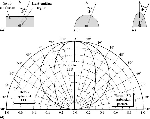
FIGURE 1.17 LEDs with (a) planar, (b) hemispherical, and (c) parabolic surfaces, and (d) far-field patterns of the different types of LEDs. At an angle of θ = 60°, the Lambertian emission pattern decreases to 50% of its maximum value occurring at θ = 0°. The three emission patterns are normalized to unity intensity at θ = 0°. (After Schubert, E.F., Light-Emitting Diodes, Cambridge University Press, Cambridge, U.K., 2003.)
GaAs1−yPy alloys with y > 0.45, which include GaP, are indirect bandgap semiconductors. The electron–hole pair recombination process occurs through recombination centers and involves excitation of phonons rather than photon emission. The radiative transitions can be enhanced by incorporating isoelectronic impurities such as nitrogen into the crystal lattice, which serve as special recombination centers. Nitrogen is from the same Group V in the periodic table as P with similar outer electronic structure. Therefore, N atoms easily replace P atoms and introduce electronic traps. As the traps are energy levels typically localized near the conduction band edge, the energy of the emitted photon is only slightly less than Eg. The radiative recombination depends on the nitrogen doping and is not as efficient as direct recombination [91,92]. The reason for the lower internal quantum efficiency for LEDs based on GaAsP and GaP:N is the mismatch to the GaAs substrate [93] and indirect impurity-assisted radiative transitions, respectively. Nitrogen-doped indirect bandgap GaAs1−yPy alloys are widely used in inexpensive green, yellow, and orange LEDs. These LEDs are suitable only for low-brightness applications only, but the green emission appears to be fairly bright and useful for many applications because the wavelength matches the maximum sensitivity of the human eye. The main application of commercial low-brightness green GaP:N LEDs is indicator lamps [94].
High-brightness green and red LEDs are based on GaInN and AlGaAs, respectively, and are suitable for traffic signals and car brake lights because their emission is clearly visible under bright ambient conditions. GaAs and Al·yGa1−yAs alloys for Al content y < 0.45 are direct-band semiconductors, and indirect for y > 0.45 [95]. The most-efficient AlGaAs red LEDs are double-heterostructure transparent-substrate devices [96,97]. The reliability and lifetime of AlGaAs devices are lower than that of AlGaInP because high-Al-content AlGaAs layers are subject of oxidation and corrosion. Being developed in the late 1980s and early 1990s, AlGaInP material system has reached technological maturity and it is today the material of choice for high-brightness LEDs emitting in the red, orange, and yellow wavelength ranges [11,98,99,100].
Traditionally, red, yellow, and, to a certain extent, green emissions were covered fairly well from the beginning of the LED history. The realization of blue LEDs, however, has been very cumbersome. Back in the 1980s, blue LEDs based on the indirect semiconductor SiC appeared on the market. However, due to low efficiency and not less important due to the high expense of these devices, SiC LEDs never achieved a breakthrough in the field of light emission. Besides SiC, direct semiconductors such as ZnSe and GaN with a bandgap at 2.67 and 3.50 eV, respectively, have been in the focus of researchers and industry. After almost 20 years of research and industrial development, the decision came in the favor of GaN, although it seems during the early 1990, that ZnSe-based device structures fabricated by SONY will finally provide blue light LEDs. The activities of Shuji Nakamura at Nichia Chemical Industries Ltd., Tokushima, Japan changed—it is fair to say overnight—everything. At the end of 1993, after gaining control over n- and p-type doping of GaN with a specifically adapted high-temperature (1000°C) two-gas-flow metal–organic chemical vapor deposition setup, Nakamura finally paved the way for commercially available blue LEDs using GaN as core material. The research on the ZnSe-based devices was abandoned because the GaN-based products were brighter by 1 order of magnitude and exhibited a much longer lifetime already at that early stage of the development. In the following, the GaInN hetero-pairing was developed to such a stage that blue and green light emitting devices became commercially available in the second half of the 1990s [101,102,103]. Nowadays, GaInN is the primary material for high-brightness blue and green LEDs.
In summary, the typical emission ranges, applications, and practical justifications of various LED material combinations are as follows: yellow (590 nm) and orange (605 nm) AlGaInP, and green (525 nm) GaInN LEDs are excellent choices for high luminous efficiency devices; Amber AlGaInP LEDs have higher luminous efficiency and lower manufacturing cost compared with green GaInN LEDs, and are preferred in applications that require high brightness and low power consumption such as solar cell-powered highway signals; GaAsP and GaP:N LEDs have the advantage of low power and low cost but posses much lower luminous efficiency, and are therefore not suitable for high-brightness applications. In general, one has to bear in mind that not only the luminous efficiency but also the total power emitted by an LED is of considerable importance for many applications. A detailed review of the optical and electrical characteristics of high-brightness LEDs is given in Refs. [5,12].
Most white-light LEDs use the principle of phosphorescence, that is, the short wavelength light emitted by the LED itself pumps a wavelength converter, which reemits light at a longer wavelength. As a result, the output spectrum of the LED consists of at least two different wavelengths. Two parameters, the luminous efficiency and the CRI, are essential characteristics for white LEDs. For example, for signage applications, the—eye catching—luminous efficiency is of primary importance and the color rendering is less important, while for illumination applications, both luminous efficiency and CRI are of equal importance. White-light sources using two monochromatic complimentary colors produce the highest possible luminous efficiency (theoretically, more than 400 lm/W) [104,105]. However, the CRI of dichromatic devices is lower than that of broadband emitters.
Most commercially available white LEDs are modified blue GaInN/GaN LEDs coated with a yellowish phosphor made of cerium-doped yttrium aluminum garnet (Ce3+:YAG) powder suspended in epoxy resin, which encapsulates the semiconductor die. The blue light from the LED chip (λ = 450–470 nm) is efficiently converted by the phosphor to a broad spectrum centered at about 580 nm (yellow). As yellow color is the complement of blue color, the combination of both produces white light. The resulting pale yellow shade is often called lunar white. This approach was developed by Nichia and has been used for the production of white LEDs since 1996 [101]. The present Nichia white LED NSSW108T (chromaticity coordinates 0.310/0.320), based on a blue LED with special phosphor, has a luminous intensity of 2.3 cd at forward voltage 3.5 V and driving current 20 mA and is intended to be used for ordinary electronic equipment (such as office equipment, communication equipment, measurement instruments, and household appliances).
The materials for effective wavelength conversion include phosphors, semiconductors, and dyes. Phosphors are stable and reliable and, therefore, most commonly used. Depending on the type, phosphors can exhibit quantum efficiencies close to 100%. The quantum efficiency of Ce3+:YAG is reported to be 75% [106]. A common phosphor consists of an inorganic host material doped with an optically active element. A well-known host material is the YAG, while the optically active dopant is a rare-earth element, typically cerium, but terbium and gadolinium are also used. The spectrum of white LED consists of the broad phosphorescence band and clearly shows the blue emission line originating from the LED chip. In order to optimize the luminous efficiency and the color-rendering characteristics of the LED, the contribution of each band can be tuned via the concentration of the phosphor in the epoxy resin and the thickness of epoxy encapsulant. The spectral output can also be tailored by substituting the cerium with other rare-earth elements, and can even be further adjusted by substituting some or all of the aluminum in the YAG with gallium.
Another phosphor-based white LED group employs tricolor phosphor blend as an optically active element and an AlGaInN UV LED emitting at 380–400 nm LED as a pump source. The tricolor phosphor blend consists of high-efficiency europium-based red and blue emitting phosphors green emitting copper and aluminum-doped zinc sulfide (ZnS:Cu, Al). Figure 1.18 shows the spectra of two white LEDs based on different pump sources: tricolor phosphor white LED (InGaAlN) and warm white LED (InGaN). The UV-pumped phosphor-based white LEDs exhibit high CRIs, typically between 60 and 80 [107]. The visible emission is solely due to phosphor, while the exact emission line of the pumping LED is not of fundamental importance. The UV-pumped white LEDs yields light with better spectral characteristics and color rendering than the blue LEDs with YAG:Ce phosphor but are less efficient. The lower luminous efficiency is due to the large Stokes shift, more energy is converted to heat in the UV-into-white-light conversion process. Because of the higher radiative output of the UV LEDs than of the blue LEDs, both approaches yield comparable brightness. However, the UV light causes photodegradation to the epoxy resin and many other materials used in LED packaging, causing manufacturing challenges and shorter lifetimes.
The third group of white LEDs, also called photon-recycling semiconductor LED (PRS-LED), is based on semiconductor converters, which are characterized by narrow emission lines, much narrower than many phosphors and dyes. The PRS-LED consists of a blue GaInN/GaN LED (470 nm) as the primary source and an electrically passive AlGaInP/GaAs double heterostructure LED as the secondary active region. The blue light from the GaInN LED is absorbed by the AlGaInP LED and reemitted or recycled as lower energy red photons [108]. The spectral output of the PRS-LED consists of two narrow bands corresponding to the blue emission at 470 nm from the GaInN/GaN LED and the red emission at 630 nm from the AlGaInP LED. Therefore, the PRS-LED is also called dichromatic LED. In order to obtain white light, the intensity of the two light sources must have a certain ratio that is calculated using the chromaticity coordinates of the Illuminant C standard [12]. In order to improve the color rendering properties of a PRS-LED, a second PRS can be added to the structure; thus, adding a third emission band and creating a trichromatic LED.
FIGURE 1.18 Emission spectra of phosphor-based white LEDs: (a) white LED (InGaAlN) with chromaticity coordinates x = 0.29 and y = 0.30 and (b) warm white LED (InGaN) with chromaticity coordinates x = 0.446 and y = 0.417. (Courtesy of Super Bright LEDs, Inc., St. Louis, MO.)
The theoretical luminous efficiency, assuming unit quantum efficiency for the devices and the absence of resistive power losses, of different types of white LEDs ranges as follows: 300–340 lm/W for dichromatic PRS-LED, 240–290 lm/W for trichromatic LED, and 200–280 lm/W for phosphor-based LED [12]. As mentioned above, on the expense of the CRI, the dichromatic PRS-LEDs have the highest luminous efficiency as compared to spectrally broader emitters.
White LEDs can also be fabricated using organic dye molecules as a wavelength converter. The dyes can be incorporated in the epoxy encapsulant [109] or in optically transparent polymers. Although dyes are highly efficient converter (with quantum efficiencies close to 100%), they are less frequently used because their lifetime is considerably shorter than the lifetime of semiconductor or phosphor wavelength converters. Being organic molecules, dyes bleach out and become optically inactive after about 104 to 106 optical transitions [12]. Another disadvantage of dyes is the relatively small Stokes shift between the absorption and the emission bands. For example, the Stokes shift for the dye coumarin 6 is just 50 nm, which is smaller than the Stokes shift of about 100 nm or more required for dichromatic white LEDs.
A research in progress involves coating a blue LED with quantum dots that glow yellowish white in response to the blue light from the LED chip.
1.4.4 SURFACE-EMITTING LEDs AND EDGE-EMITTING LEDs
There are two basic types of LED emitting configurations: surface-emitting LEDs and edge-emitting LEDs. Schematic illustrations of both structures and the corresponding emission patterns are given in Figure 1.19. The light output of surface-emitting LEDs exits the device through a surface that is parallel to the plane of the active region, while an edge-emitting LED emits light from the edge of the active region. A quick comparison between both LED configurations shows that surface emitters have relatively simpler structure and are less expensive but have much larger emitting area (circular area with diameters of typically 20–50 μm). Therefore, the total LED optical output power is as high as or higher than the edge-emitting LEDs. However, the larger emitting area in addition to the Lambertian radiation emission pattern (light is emitted in all directions) and the low-to-moderate operating speeds impose limitations on the use of surface-emitting LEDs in fiber-optic communication systems, which require fast response time and high coupling efficiency to the optical fiber.
High-brightness LEDs, or power LEDs, are surface-emitting LEDs with optimized heat removal, allowing much higher power levels. High-brightness LEDs operate at high forward current. The higher driving current results in slight red shift of the peak wavelength caused by heating the chip. Power LEDs produce significant amounts of heat, which can reduce lumen output or cause device failure. Therefore, the LED design has to implement careful thermal control and effective heat removal. The power LEDs packaging incorporates a heat sink slug, which transfers heat from the semiconductor chip to the external heat sink with high efficiency. Liquid cooling allows the most powerful LEDs to run at their limits, while safeguarding operating life and maximizing instantaneous output. In power LEDs, fully integrated smart control manages the current to avoid overdrive.
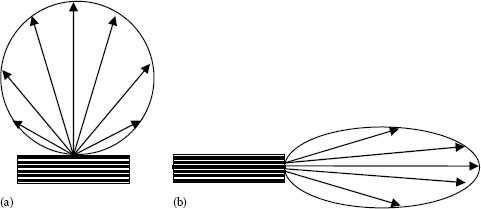
FIGURE 1.19 (a) Surface-emitting LED and (b) edge-emitting LED, and the corresponding far-field radiation patterns.
Resonant-cavity LEDs (RCLEDs) are essentially highly optimized surface-emitting LEDs with a small area of the active region. RCLEDs have more complicated construction involving an active region of multiquantum-well structure and two distributed Bragg reflectors, which form an optical cavity. GaInP/AlGaInP RCLEDs emit at 650 nm and are appropriate for optical communications using plastic optical fibers that can have core diameters as large as 1 mm. In comparison with conventional LEDs, RCLEDs exhibit high brightness, narrow spectral width, higher spectral purity, low beam divergence, and therefore, higher coupling efficiency and substantially higher fiber-coupled intensity [110,111]. High-speed transmission of 250 Mbit/s over plastic optical fibers has been obtained with RCLEDs emitting at 650 nm [112].
Edge-emitting LEDs offer high-output power levels and high-speed performance but are more complex and expensive, and typically are more sensitive to temperature fluctuations than surface-emitting LEDs. The multilayered structure of an edge-emitted LED acts as a waveguide for the light emitted in the active layer. Current is injected along a narrow stripe of active region producing light that is guided to the edge, where it exits the device in a narrow angle. As the light emanates from the edge of the active area, the emitting spot is very small (<20 μm2), the LED output power is high, and a strongly directed emission pattern is obtained. Typically, the active area has a width less than 10 μm and thickness not more than 2 μm. The light emitted at λ = 800 nm from such an area would have a divergence angle about 23°, which is poor in comparison with a strong directional laser beam, but much higher than surface-emitting LEDs. Edge-emitting LEDs deliver optical power at most several microwatts, compared to milliwatts for laser diodes (power collected by a collection numerical aperture of 0.1). However, the small emission area and relatively narrow emission angles result in brightness levels 1–2 orders of magnitude higher than comparable surface-emitting LEDs. As an example, a surface-emitting LED with an area diameter of 100 μm delivering 5 mW of total optical power would put less than 0.05 μW into an optical fiber with numerical aperture of 0.1. The high-brightness, small emitting spot and narrow emission angle allow effective light coupling to silica multimode fibers with typical core diameters of 50–100 μm. The light intensity emitted by the LED is directly proportional to the length of the waveguide (the stripe of the active region). However, the electrical current required to drive the LED also increases with the stripe length, and when the current reaches sufficiently high level, stimulated emission takes place.
Superluminescent diodes (SLDs) are edge-emitting LEDs, which operate at such high current levels that stimulated emission occurs. The current densities in SLD are similar to that of a laser diode (~kA/cm2). The emission in a SLD begins with a spontaneous emission of a photon because of radiative electron–hole recombination. Sufficiently, strong current injection creates conditions for stimulated emission. Then, the spontaneously emitted photon stimulates the recombination of electron–hole pair and the emission of another photon, which has the same energy, propagation direction, and phase as the first photon. Thus, both photons are coherent. In contrast to LEDs, the light emitted from an SLD is coherent, but the degree of coherence is not so high compared to laser diodes and lasers. SLDs are a cross between conventional LEDs and semiconductor laser diodes. At low current levels, SLDs operate like LEDs, but their output power increases super linearly at high currents. The optical output power and the bandwidth of SLDs are intermediate between that of an LED and a laser diode. The narrower emission spectrum of the SLDs results from the increased coherence caused by the stimulated emission. The FWHM is typically about 7% of the central wavelength.
SLDs comprise a multiquantum-well structure and the active region is a narrow stripe, which lies below the surface of the semiconductor substrate. In an SLD, the rear facet is polished and highly reflective. The front facet is coated with antireflection layer, which reduces optical feedback and allows light emission only through the front facet. The semiconductor materials are selected such that the cladding layers have greater bandgap energies than the bandgap energy of the active layer, which achieves carrier confinement, and smaller refractive indices than the refractive index of the active layer, which provides light confinement. If a photon, generated in the active region, strikes the surface between the active layer and the cladding layer at an angle smaller than the critical angle of TIR, it will leave the structure and will be lost. The photons that undergo TIR are confined and guided in the active layer like in a waveguide. SLDs are similar in geometry to semiconductor lasers but lack the optical feedback required by laser diodes.
The development of SLDs was in response to the demand for high-brightness LEDs for higher bandwidth systems operating at longer wavelengths, and that allow for high-efficiency coupling to optical fibers for longer distance communications. SLDs are suitable as communication devices used with single-mode fibers, as well as high-intensity light sources for the analysis of optical components [113]. SLDs are popular for fiber-optic gyroscope applications, in interferometric instrumentation such as optical coherence tomography (OCT), and in certain fiber-optic sensors. SLDs are preferred to lasers in these applications, because the long coherence time of laser light can cause troublesome randomly occurring interference effects.
Organic LEDs (OLEDs) employ an organic compound as an emitting layer, which can be small organic molecules in a crystalline phase or conjugated polymer chains. To function as a semiconductor, the organic emitting material must have conjugated π-bonds. Polymer LEDs (PLEDs) can be fabricated in the form of thin and flexible light-emitting plastic sheets and are also known as flexible LEDs.
The OLED structure features an organic heterostructure sandwiched between two inorganic electrodes (typically, calcium and indium tin oxides). The heterostructure represents two thin (≈100 nm) organic semiconductor films, a p-type transport layer made of triphenyl diamine derivative and an n-type transport layer of aluminum tris(8-hydroxyquinoline) [58]. A glass substrate may carry several heterostructures that emit different wavelengths to provide a multicolor OLED. A white OLED uses phosphorescent dopants to create green and red lights and a luminescent dopant to create blue light, and also to enhance the quantum efficiency of the device. The three colors emerge simultaneously through the transparent anode and glass substrate. White OLEDs exhibit nearly unity quantum efficiency and good color rendering properties. Higher brightness requires a higher operating current and, thus, a trade-off in reliability and lifetime. An improved OLED structure uses a microcavity tandem in order to boost the optical output and reduce the operating current of OLEDs [114]. The result was an enhancement of the total emission by a factor of 1.2 and of the brightness by a factor of 1.6. This seems significant, especially when considering the simplicity of the design change compared with methods such as incorporation of microlenses, microcavities, and photonic crystals.
PLEDs have similar structure, and the manufacturing process uses a simple printing technology, by which pixels of red, green, and blue materials are applied on a flexible substrate of polyphenylene vinylene. Compared to OLEDs, PLEDs are easier to fabricate and have greater efficiencies, but offer limited range of colors. In comparison with inorganic LEDs, LEDs are lighter, flexible, rollable, and generate diffuse light over large areas, but have substantially lower luminous efficacy. The combination of small organic molecules with polymers in large ball-like molecules with a heavy-metal ion core is called a phosphorescent dendrimers [58]. The connoisseurs distinguish between the technological processes, device structures and characteristics, and use the acronym OLEDs only when they refer to small-molecules OLEDs, while in the mass media and daily life the term OLEDs is used also for PLEDs.
OLEDs have amazing potential for multicolor displays, because they provide practically all colors of the visible spectrum, high resolution, and high brightness achieved at low drive voltages/current densities, in addition to a large viewing angle, high response speeds, and full video capability. For example, the Kodak display AM550L on a 2.2 in. screen features 165° viewing angle that is up to 107% larger than the LCDs on most cameras. The operating lifetime of OLEDs exceeds 10,000 h.
OLEDs are of interest at low-cost replacements for LCDs because they are easier to fabricate (fewer manufacturing steps and, more importantly, fewer materials used) and do not require a backlight to function, potentially making them more energy efficient. The backlighting is crucial to improve brightness in LCDs and requires extra power, which, for instance, in a laptop translates into heavy batteries. In fact, OLEDs can serve as the source for backlighting in LCDs.
OLEDs have been used to produce small-area displays for portable electronic devices such as cell phones, digital cameras, MP3 players, and computer monitors. The OLED display technology is promising for thin TVs, flexible displays, transparent monitors (in aviation and car navigation systems), and white-bulb replacement, as well as decoration applications (wall decorations, luminous clothing, accessories, etc.). Larger OLED displays have been demonstrated, but are not practical yet, because they impose production challenges in addition to still too short lifetime (<1000 h). Philips’ TF PolyLED technology is promising for the production of full color less than 1 mm thick information displays.
In a most recent announcement [115], OSRAM reported record values of efficiency and lifetime and a simultaneous improvement of these two crucial OLED characteristics while maintaining the brightness of a white OLED. OSRAM reported that under laboratory conditions, warm white OLED achieved efficiency of 46 lm/W (CIE color coordinates x/y of 0.46/0.42) and a 5000 h lifetime, at a brightness of 1000 cd/m2. The large-scale prototype lights up an area of nearly 90 cm2. With this improvement, flat OLED light sources are approaching the values of conventional lighting solutions and open new opportunities for application.
The breakthroughs in LED technologies and the following rapid expansion of the LED market demanded accurate photometric techniques and photometric standards for LED measurement. LED metrology is an important tool for product quality control, as well as a prerequisite for reliable and sophisticated LED applications. CIE is currently the only internationally recognized institution providing recommendations for LED measurements. The basics of LED metrology are outlined in the CIE Publication 127 Measurements of LEDs [116]. Practical advices and extensive description of LED measurements and error analysis are presented also in Ref. [117]. Four important conditions must be met when performing light measurements on LEDs with accuracies better than 10%: CIE-compatible optical probe for measuring the relevant photometric parameter, calibration equipment traceable to a national calibration laboratory, high-performance spectroradiometer (with high dynamic measuring range and precision), and proper handling. The characteristics of optical measuring instruments, photometers, and spectroradiometers are presented in Chapter 3. We limit the considerations here only to measuring optical characteristics, and omit measurements of electrical parameters.
1.4.6.1 Measuring the Luminous Intensity of LEDs
The most frequently measured parameter of an LED is luminous intensity. The definition of intensity and the underlying concept for measuring radiant and luminous intensity assumes a point light source. Although an LED has a small emitting surface area, it cannot be considered as a point source, because the LED area appears relatively large compared to the short distance between the detector and the LED that is typically used for the intensity measurements. Thus, the inverse square law that holds for point source does no longer hold for an LED, and cannot be used for calculating radiant intensity from irradiance. Therefore, the CIE has introduced the concept of averaged LED intensity, which relates to a measurement of illuminance at a fixed distance [116]. The CIE specifies the conditions for measuring luminous intensity in different laboratories irrespective of the design of the LED. The LED should be positioned in such a way that its mechanical axis is directly in line with the center point of a round detector with an active area of 1 cm2, and the surface of the detector is perpendicular to this axis. The distance between the LED and the detector surface should be measured always from the front tip of the LED. The CIE recommends two geometries for measuring luminous intensity. Condition A sets the distance between LED tip and detector equal to 316 mm and a solid angle of 0.001 sr, while Condition B uses distance between LED tip and detector of exactly 100 mm and a solid angle of 0.01 sr. Condition B is suitable also for weak LEDs, and therefore, is used more often than Condition A. Both geometries require the use of special intensity probes. For example, the LED-430 measuring adapter developed by Instrument Systems LED-430 is used with Condition B (100 mm), whereas the LED-440 probe conforms to Condition A for bright LEDs with a very narrow emission angle.
1.4.6.2 Measuring the Luminous Flux of LEDs
Two principal methods are used for measuring the luminous flux of LEDs: the integrating sphere, which integrates the total luminous flux, and the goniophotometer, which measures the radiation beam of the LED at different θ and φ angles with subsequent calculation of total luminous flux.
The first method, shown on Figure 1.20, employs a hollow sphere with a diameter of 80 or 150 mm with a port for the LED and a baffled port for the detector positioned at 90° with respect to the LED port. The interior of the sphere is coated with a very stable material that ensures diffuse reflection of the LED light. After multiple reflections, the light is captured by the detector, and the measured irradiance E is proportional to the launched total radiant flux Φ. This applies only to the ideal case when the interior of the sphere has a Lambertian characteristic with constant reflectance over the entire interior of the sphere and constant spectral properties, the detector has perfect cosine correction, and there are no absorbing surfaces in the sphere [118]. However, in reality, the diffuse reflector is not perfect; also, the spectral characteristics of the coating and the size of the ports are sources of error. The main factor determining the luminous-flux measurement accuracy is the wide range of radiation characteristics of LEDs. An accuracy of about 5% can be obtained for LEDs with diffuse emission, but deviations of more than 10% are possible for LEDs with narrow emission angle. The larger sphere is used when it is important to keep measurement errors to a minimum, because the ratio of the sphere area to the size of the ports and the LED is more favorable [117]. However, the larger area results in a loss of intensity.
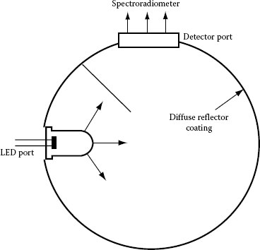
FIGURE 1.20 Cross-section of an integrating sphere.
The second method, the goniophotometer, uses a cosine-corrected detector that moves on an imaginary sphere of radius r enclosing the LED. The detector measures the irradiance E as the partial radiant flux dΦ incident on a detector area dA as a function of θ and φ. The angles θ and φ vary from 0° to 360°. The total radiant power Φ is obtained by integrating the irradiance over the entire sphere surface. Alternatively, instead of moving the detector, which requires mechanical adjustments, the LED can be rotated about its tip. The CIE recommended distance LED—detector is 30 cm, the area of the detector should be 1 cm2 in the case of diffuse LEDs, and should be reduced for measurements of narrow-angled LEDs. The goniophotometer provides greater accuracy than the integrating sphere, which includes numerous geometric and spectral sources of error, in particular the wide range of radiation characteristics of LEDs.
1.4.6.3 Mapping the Spatial Radiation Pattern of LEDs
Different packages and types of LEDs exhibit different far-field radiation patterns. The spatial distribution of the emitted radiation is an important LED characteristic for many applications, in particular, for full-color (red, green, and blue) LED displays in which color balance can change when the display is observed off axis. Careful analysis of the radiation pattern is important also for white LED applications: the color coordinates of a white LED often show a significant blue shift due to the angle dependence of the light path through the phosphor. The method used to map the LED radiation pattern involves a goniometer. The LED is pivoted about its tip and the intensity is recorded at different angles providing at first the profile of the radiated beam in one plane. After that, the LED is rotated about its mechanical axis in order to obtain the two-dimensional radiation pattern.
1.4.6.4 LED Measuring Instrumentation
LED metrology is based on two measuring procedures: the spectral resolution method based on a spectroradiometer and the integration method based on a photometer. In the first method, a spectroradiometer measures the total spectral power distribution of the LED and the photometric value of interest is determined from the measured spectrum using standard CIE tables and a special software. In the second method, a photometer, which employs a broadband detector in conjunction with a V(λ) filter, is used. Photometers are calibrated for measuring a specific photometric quantity, that is, the output current of the detector is directly proportional to the photometrically measured value. For example, a photometer for luminous intensity is calibrated in candela per photocurrent. The V(λ) filters are optimized for the spectral radiation distribution of a standard illuminant A light source (a Planckian radiator with 2850 K color temperature), which is maximum in the IR region. LEDs, however, have a completely different spectral power distribution, with respect to emission line shape, FWHM, and specific peak wavelength. Because of the inadequate correction of the V(λ) filter in the visible and the blue part of the spectrum, industrial photometers are not recommended for testing blue, deep red, and white LEDs. Therefore, spectroradiometers are more suitable for LED metrology. The absolute calibration of the spectroradiometer should be done with a standard LED traceable to a national calibration laboratory. The spectral resolution of a spectrometer (the bandpass) should be approximately 1/5 of the FWHM of the LED.
Only an LED can be used as a reference for absolute calibration of the intensity probe for LED measurements. An accurate calibration of the measuring instrumentation designed for a given type of light sources can be obtained only with a reference standard source from the same group with similar characteristics. In general, an absolute calibration of a detector for irradiance employs a broadband light source, such as a standard halogen lamp, traceable to a national calibration laboratory, and calculates the radiant intensity from irradiance using the inverse square law. However, LEDs are not point light sources under CIE standard measuring conditions and the inverse square law does not hold. In addition, their spectral distribution and radiation characteristics differ considerably from those of a halogen lamp. Therefore, such lamps are not suitable for absolute calibration of LED measuring instrumentation. For this purpose, standard temperature-stabilized LEDs with Lambertian radiation characteristics are used [117]. The value for luminous intensity or radiant intensity of these standards has to be determined by a national or international calibration authority.
Apart from the spectrometer, other external factors that influence strongly the measuring accuracy of LEDs are the ambient temperature, forward voltage stabilization, and careful handling. The temperature stabilization time of an LED depends on the type of the LED and the ambient temperature. To assure high accuracy, the measurements should be performed after a steady state of the LED has been attained, which can be identified by the forward voltage of the LED. The stability and accuracy of the current source should be taken into account, because a deviation of 2% in the current, for example, causes more than 1% change in the value for luminous intensity of a red LED. Careful handling and precise mechanical setup are essential for high accuracy and reproducibility of the LED measurements. A deviation of 2 mm in the distance LED detector leads to an error in the luminous intensity measurement of approximately ±4%. The quality of the test socket holding the LED is very important especially for clear, narrow-angled LEDs, where reproducible alignment of the mechanical axis of the LED is crucial for reproducible measurement of luminous intensity [117].
The LED characterization in the production flow imposes additional requirements to detectors and measurement time. Array spectroradiometers are now preferable for production control of LEDs because of significant increase in sensitivity and quick response time due to employment of high-quality back-illuminated CCD sensors. The compact array spectrometer CAS140B from Instrument Systems GmbH is an efficient measuring tool that permits luminous intensity (cd), luminous flux (lm), color characteristics (color coordinates, color temperature, and dominant wavelength), and the spatial radiation pattern of LEDs to be determined using just one instrument. It features measuring times of a few tens of milliseconds and high level of precision necessary for evaluating the optical parameters of LEDs. It can be used for development and quality assurance in areas where LEDs need to be integrated in sophisticated applications (e.g., in the automotive and avionics sector and in displays and the lighting industry).
Usually, the test time of an LED under production conditions is in the order of a few milliseconds. This period is shorter than the temperature stabilization time for most LED types and is not sufficient to guarantee a measurement of the LED in a steady state. Although, the values measured under production conditions differ from those obtained under constant-current conditions, there is generally a reproducible correlation between them, which is used for proper correction of the values measured in production testing.
During the last decades, the LED concept underwent a tremendous development. The LED market has grown over the past 5 years at an average rate of 50% per year and forecasts to reach $90 million by 2009 [119]. Because of the increasing brightness and decreasing cost, LEDs find countless everyday applications—from traffic signal lights to cellular phone and digital camera backlighting, in automotive interior lighting and instrument panels, giant outdoor screens, aviation cockpit displays, LED signboards, etc. In 2005, the cell-phone applications held the highest share (52%) of the highbrightness LED market, followed by LCD backlighting (11.5%), signage (10.5%), and automotive applications (9.5%). Besides the rapid progress and recent advance of white LEDs, the LED illumination market is still low at 5.5%, because the consumer is not familiar yet with the advantages and possibilities of solid state lighting. LEDs in traffic lights held 4.5%, and 7% of the LED market included other niche applications [120]. The five manufacturers who currently dominate the market are Lumileds Lighting LLC, Osram Opto Semiconductors, Nichia Corp., Cree Inc., and Toyoda Gosei Co. Ltd.
The applications of LEDs can be grouped roughly by the emission spectral range. LEDs emitting in the IR range (λ > 800 nm) find applications in communication systems, remote controls, and optocouplers. White LEDs and colored LEDs in the visible range are of main importance for general illumination, indicators, traffic signal lights, and signage. UV LEDs (λ < 400 nm) are used as pump source for white LEDs, as well as in biotechnology and dentistry. Superluminescent LEDs (SLEDs) were developed originally for the proposes of large luminescent displays and optical communication, but quickly found numerous novel applications as an efficient light source in the fields of medicine, microbiology, engineering, traffic technology, horticulture, agriculture, forestry, fishery, etc. SLEDs are the latest trend in general and automotive lightings.
For a comprehensive introduction to lighting technology and applications of solid-state sources, see Žukauskas et al. [5]. Here, we briefly cover few more high-brightness LED illumination applications that were not included in the previously mentioned review.
The main potential of white LEDs lies in general illumination. Penetration of white LEDs into the general lighting market could translate (globally) into cost savings of $10 [11] or a reduction of power generation capacity of 120 GW [90].
The strong competition in the field has fueled the creation of novel device architectures with improved photon-extraction efficiencies, which in turn have increased the LED’s brightness and output power. In September 2007, Cree, Inc. (Durham, NC) demonstrated light output of more than 1000 lm from a single R&D LED—an amount equivalent to the output of a standard household light bulb. A cool-white LED at 4 A delivered 1050 lm with efficacy of 72 lm/W. The LED operated at substantially higher efficacy levels than those of today’s conventional light bulbs.
In response to this challenge, in October 2007, Philips Lumileds launched the industry’s first 1 A LED called LUXEON K2 with thin-film flip chip (TFFC) LED [121]. This cool-white LED is designed, binned, and tested for standard operation at 1000 mA and capable of being driven at 1500 mA. LUXEON K2 with TFFC operates only at 66% of its maximum power rating and delivers unprecedented performance for a single 1 mm2 chip: light output of 200 lm and efficacy over 60 lm/W (5 W) at 1,000 mA, and after 50,000 h of operation at 1,000 mA, it retains 70% of the original light output. The TFFC technology combines the advantages of InGaN/GaN FCdesign by Philips Lumileds, with a TF structure to create a higher-performance TFFC LED [122]. At present, LUXEON K2 with TFFC is the most robust and powerful LED available on the market, offering the lowest cost of light with the widest operating range. Another LED product of Philips Lumileds, LUXEON Rebel LED (typical light output of 145 lm of cool-white light at 700 mA, CCT 4100 K, and Lambertian radiation pattern), is the smallest surface mountable power LED available today. With thickness of the package of only 2.6 mm, the ultracompact LUXEON Rebel is ideal for both space-constrained and conventional solid-state lighting applications.
Nowadays, white LEDs are used as a substitution for small incandescent lamps and of strobe light in digital cameras, in flashlights and lanterns, reading lamps, emergency lighting, marker lights (steps and exit ways), scanners, etc. Definitely, LEDs will widely displace incandescent light bulbs because of the comparably low power consumption and versatility of technological adaptation. The luminous flux per LED package has increased by about four orders of magnitude over a period of 30 years [5,90], and the performance of commercial white LEDs marked a tremendous progress in the last few years. However, in times of growing environmental and resource saving challenges, it is still far from complete satisfaction of the constantly increasing requirements of the general illumination market.
Other applications of white LEDs are for backlighting in LCD, cellular phones, switches, keys, illuminated advertising, etc. White LEDs, like high-brightness colored LEDs, can be used also for signage and displays, but only in low ambient-illumination applications (night-light).
Power LEDs enable the design of high-intensity lighting systems for industrial machine-vision applications such as line lights for inspection of printed circuit boards, wafers, glass products, and high-speed security paper. The illumination systems in machine vision typically use high-intensity discharge bulbs, which provide several thousand lumens of light, but also generate a lot of heat. Therefore, the HID lamps in these systems are always combined with a fiber optic to distance the target from the bulb. When the application requires monochromatic lighting, filters have to be used, which reduce the intensity output. In addition, HID bulbs are expensive, last only few thousand hours, and suffer intensity and color changes during their lifetimes. Nowadays, many of the HID-lamp illumination systems in machine vision are replaced with power LED-based lighting systems that are able to provide intensities exceeding those of HID systems. LEDs-based systems are cheaper to buy, maintain, and run. LEDs are capable of 100,000 h of operation and their intensity remains constant during their lifetime. In comparison with other light sources, which require as much as 100 V for operation, LEDs have nominal voltage typically of 1.5 V for a nominal current of 100 mA. Thanks to many advantages LED lighting offers, it is becoming the standard in metrology applications.
1.4.7.2 LED-Based Optical Communications
LEDs can be used for either free-space communication or short- and medium-distance (<10 km) optical fiber communications. The basics of free-space communication and optical fiber communications are outlined in Refs. [123,124]. Free-space communication is usually limited to direct line of sight applications and includes the remote control of household appliances, data communication via IR port between a computer and peripheral devices, etc. The light should be invisible to prevent distraction; hence, GaAs/GaAs (~870 nm) or GaInAs/GaAs (~950 nm) LEDs emitting in the near IR are appropriate for this application. The total light power and the far-field emission pattern are the important LED parameters for free-space communication applications. The LED output determines the transmission distance, usually less than 100 m, although distances of several kilometers are also possible at certain conditions. The Lambertian emission pattern provides wider span of the signal and more convenience for the user, because it reduces the requirement of aiming the emitter toward the receiver.
Optical-fiber communications employ two types of optical fibers: single-mode and multimode fibers. Only fibers with small core diameter (in the order of a few micrometers) and small numerical apertures can operate as a single-mode fiber. For example, a silica-glass fiber with refractive index n = 1.447 and numerical aperture NA = 0.205 can operate as a single-mode fiber at wavelength λ = 1.3 μm, if the core diameter of the fiber is less than 4.86 μm. The small-core diameter and numerical aperture impose stringent requirements to the light beam diameter, divergence, and brightness. High coupling efficiency of the light emanating from the LED to the fiber can be attained if the light emitting spot is smaller than the core diameter of the optical fiber. Although SLEDs are occasionally used with single-mode fibers, LEDs do not provide sufficiently high LED-fiber coupling efficiency to compete with lasers. However, LEDs can meet the requirements for multimode (graded-index or step-index) fiber applications. Silica multimode fibers have core diameters of 50–100 μm, while the plastic fibers diameter could be as large as 1 mm. Thus, the LEDs that have typically circular emission regions with diameters of 20–50 μm are suitable for devices with multimode fibers. Surface-emitting RCLEDs based on AlGaInP/GaAs material system and emitting in the range 600–650 nm are useful for plastic optical fiber communications. Edge-emitting superluminescent InGaAsP/InP LEDs emitting at 1300 nm are used with graded-index silica fibers for high-speed data transmission.
The LED exitance (power emitted per unit area) is useful figure of merit for optical-fiber communication applications. It determines the transmission distance in the fiber. LED-based optical-fiber communication systems are suited for low and medium data-transmission rates (<1 Gbit/s) over distances of a few kilometers. The limitation imposed on the transmission rate is related to the LED response time.
Response time is a very important characteristic, especially for LEDs used in optical communication applications. A light source should have short enough response time in order to meet the bandwidth limits of the system. The response time is determined by the source’s rise (switch on) or fall (switch off) time of the signal. The rise time is the time required for the signal to go from 10% to 90% of the peak power. The turn-off time of most LEDs is longer than the turn-on time. Typical values for LED turn-off times are 0.7 ns for the electrical signal and 2.5 ns for the optical signal. SLEDs used in optical communications have a very small active area, much smaller than the die itself (thus, small diode capacitance), and the response time is determined by the spontaneous recombination lifetime (the fall time). For a resonant-cavity LED at room temperature, the response time ranges from about 3 to 1.1 ns for voltage swing Von − Voff = 0.4–1.4 V [12,125]. The response time of about 1 ns in highly excited semiconductors limits the maximum transmission rate attainable with LEDs below 1 Gbit/s. However, transmission rates of several hundred megabits per second are satisfactory for most local-area communication applications. Lasers and laser diodes are used for higher bit rates and longer transmission distances.
1.4.7.3 Applications of the LED Photovoltaic Effect
1.4.7.3.1 Photovoltaic Effect
In addition to high efficiency and brightness of several candelas, superbright LEDs (SBLEDs) exhibit a remarkably large photovoltaic effect, as large as a conventional Si photodiode, which suggests that a SBLED has an excellent ability to function as a photodiode [126]. Figure 1.21 shows the photoemission and photoreception spectra of red LED at room temperature. The photovoltaic effect was demonstrated with a pair of two identical red (660 nm) SBLEDs (Stanley H-3000, brightness of 3 cd, and rated current of 20 mA). As shown in Figure 1.22, one of the LEDs was the emitter, the other played the role of a receiver. Figure 1.23 compares the photocurrent Ip of a SBLED H3000 with the photocurrent of a typical Si photodiode (TPS708): the LED photocurrent is approximately 1/3 of the photocurrent for the Si photodiode. However, this does not mean that the SBLED as photodetector is inferior to the Si photodiode. Since the LED photovoltage is 1.5 V for a current through the first LED I1 = 20 mA and about three times of that of the Si photodiode (0.5 V), the LED has almost an equal ability with respect to the conversion of optical radiation to electrical energy, at least at this wavelength (660 nm). In addition, the light-receiving ability is approximately proportional to the brightness (cd) of LED and GaAlAs-system red LED exhibits the largest light-receiving ability.
1.4.7.3.2 LED/LED Two-Way Communication Method
On the basis of the LED photovoltaic effect, a new two-way LED/LED system for free-space communication was developed [127]. Each LED in the two-way optical transmission system plays a twofold role: of a light source and of a photo-receiver. The system, consisting of a pair of SBLEDs (660 nm GaAlAs) and a pair of bird-watching telescopes, was demonstrated for free-space optical transmission of an analogue audio signal (radio signal) at a distance of 5 km. Instead of telescopes, a pair of half-mirror reflex cameras were used later in a versatile reciprocal system for long-distance optical transmission of analogue signals [128]. The employment of the reflex cameras eases the collimation of the light beam and alignment of the optical axis, and as a result, multiple communications are possible.
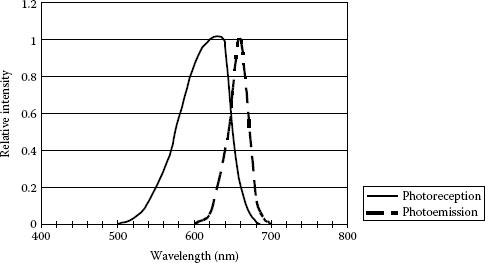
FIGURE 1.21 Photoemission and photoreception spectra of red LED (Toshiba TLRA190P) at room temperature. (From Okamoto, K., Technical Digest, The International PVSEC-5, Kyoto, Japan, 1990. With permission.)
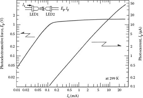
FIGURE 1.22 Photovoltaic effect between two LEDs. (From Okamoto, K., Technical Digest, The International PVSEC-5, Kyoto, Japan, 1990. With permission.)
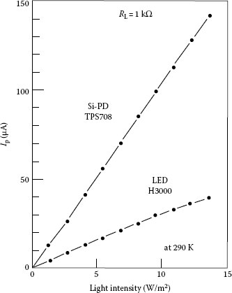
FIGURE 1.23 Comparison of photocurrent Ip between SBLED H3000 and a typical Si p−n photodiode TPS708. (From Okamoto, K., Technical Digest, The International PVSEC-5, Kyoto, Japan, 1990. With permission.)
1.4.7.3.3 LED Solar Cell
Using both, the high-efficient luminescence and the large photovoltaic effect of the SBLEDs, Okamoto developed a new type of solar cell, named LED CELL, which was the world-first reversible solar cell [126]. A later version, the 7 W LED CELL III [129], consisted of 3060 pieces of red SBLEDs (Toshiba TLRA190P, GaAlAs system, light intensity of 7 cd, wavelength of 660 nm, and diameter of 10 mm) and provided an open circuit voltage Vo = 1.6 V and a short circuit current Is = 2 mA for sunshine of 120 klux. This electric power could drive as many as several hundreds of wrist watches. The cell is a stand-alone one, equipped with batteries, solar sensor, sun-tracking mechanism, and control circuit. The output voltage of the cell is adjustable between 1.5 and 12 V, and the maximum electric power is about 5 W. The LED cell not only generates electricity but also emits dazzling red-color light in a reversible manner. Figure 1.24 shows the I–V curve of LED CELL III. The LED solar cell exhibits a good rectangular I–V curve with fill factor of about 0.85, which is better than a Si-crystal solar cell of about the same electric power. The conversion efficiency of the single LED (7 cd, GaAlAs, and 10 mm) is 4.1%, whereas the efficiency of LED CELL III is 1.5% [128].
1.4.7.3.4 Photo-Coupler
Using the photovoltaic effect of SBLED, a new type of photo-coupler or photo-relay can be realized. Because of the large induced photovoltage, the effect is especially favorable for the voltage-drive type photo-coupler or photo-relay. Figure 1.25 shows a two-way (reversible) photo-coupler composed of SBLEDs only [126]. In this photo-coupler, each side has three SBLEDs connected in series. The photo-coupler produces a photovoltage as high as 1.5 × 3 = 4.5 V for a small primary input current of 1 mA or less, therefore the output can drive a CMOS-IC directly. The photo-coupler has a particularly convenient feature: it works in any direction and there is no need to pay attention to its direction upon mounting onto a socket or attaching it onto a circuit plate.
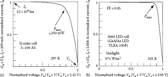
FIGURE 1.24 Comparison of a Si solar cell and LED CELL III: (a) I−V curve of a crystal Si solar cell for sunlight of 120,000 lux and (b) I−V curve of the 3060 pieces LED CELL III. (From Okamoto, K. and Tsutsui, H., Technical Digest, The International PVSEC-7, Nagoya, Japan, 1993. With permission.)
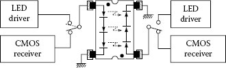
FIGURE 1.25 Two-way (reversible) photo-coupler composed only of LEDs capable of direct drive of CMOS-IC. (From Okamoto, K., Technical Digest, The International PVSEC-5, Kyoto, Japan, 1990. With permission.)
1.4.7.3.5 LED Translator
The SBLED emits light with enough intensity even for a low-level input current of the order of several hundreds microamperes. On the other hand, it generates a large photovoltage. Therefore, if two SBLEDs are connected in parallel (with the same polarity) and one of them is illuminated by light with enough intensity, then the other SBLED will light up. This was implemented in a signal translator with two-way mode as shown in Figure 1.26 [126]. Similarly, if three SBLEDs are connected in parallel like in Figure 1.27, optical signals or data can be transmitted freely among the three LED terminals.
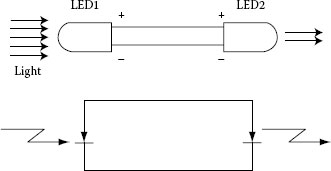
FIGURE 1.26 Light signal translator using two SBLEDs. (From Okamoto, K., Technical Digest, The International PVSEC-5, Kyoto, Japan, 1990. With permission.)
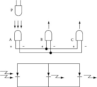
FIGURE 1.27 Data bus using three SBLEDs. (From Okamoto, K., Technical Digest, The International PVSEC-5, Kyoto, Japan, 1990. With permission.)
1.4.7.4 High-Speed Pulsed LED Light Generator for Stroboscopic Applications
Due to their large dc power capacity, SBLEDs offer large and stable intensity output when operated in ultrashort pulsed mode. On this basis, a high-speed pulsed light generator system was developed for optical analysis and imaging of fast processes in fluid dynamics [130]. The system was demonstrated with a red Toshiba SBLED (TLRA190P) in pulsed operation at charging voltage of 200 V and driving current 30 A, pulse duration of 30 ns and pulse repetition rate 100 Hz. The pulse repetition rate is up to 1 kHz and the pulse width can be adjusted in the range 20–100 ns. Under pulsed operation, this diode emits at about 660 nm with FWHM of about 25 nm. The maximum light power generated by the LED is 1.5 W. Due to the pronounce coherence, this type of LEDs are especially suited for stroboscopic methods. An integrated lens reduces the aperture of the light beam to approximately 10°. If the object to be illuminated is easily accessible, the LED can be installed without any additional optics. The pulsed light generator system was used in stroboscopic applications such as spray formation and evaporation of a jet of diesel fuel injected under diesel engine conditions into a chamber (typical velocities of such a flow field are in the range of 100–200 m/s).
1.4.7.5 LED Applications in Medicine and Dentistry
The most common applications of LEDs in medicine and dentistry are in custom-designed modules for replacement of mercury lamps. These modules employ UV and deep-UV LEDs grown on sapphire substrates and emitting in the range of 247–385 nm. For example, Nichia’s NCSU034A UV LED with peak wavelength at 385 nm offers optical power of 310 mW at typical forward voltage 3.7 V and driving current of 500 mA and has an emission angle of 240°. The LED systems are used for surgical sterilization and early detection of teeth- or skin-related problems, in biomedical and laboratory equipment, for air and water sterilizations. Nowadays, high-brightness blue LED illumination is widely used for photoinduced polymerization of dental composites [131].
The U.S. firm Lantis Laser has developed a new noninvasive imaging technique, OCT, which employs an InP-based superluminescent UV LED. The OCT instrument is used by dentists to detect early stages of teeth disease before they show up on an x-ray; hence, less-damaging treatment of diseased teeth. This is possible, because the spatial resolution of the three-dimensional images produced by OCT is 10 times better than an x-ray. One reason for this is that x-ray detection of tooth decay depends on a variation in material density, a sign that damage has already been done, whereas OCT relies on more subtle variations in optical characteristics.
An original research has shown that irradiation with blue and green SBLEDs may suppress the division of some kind of leukemia and liver cancer cells, for instance, the chronic myelogenous cell, K562, and the human acute myelogenous leukemia cell, KG-1 [132,133]. The commonly used method of photodynamic therapy (PDT) aims to destroy cancerous cells through photochemical reactions induced by a laser light in photosensitive agents, such as metal-free porphyrins, which have an affinity toward cancerous cells. There are two typical medical porphyrins: porfimer sodium (Photofrin) is used with an excimer laser and talaporfin sodium (Laserphyrin) is used with a laser diode with wavelengths 630 and 660 nm, respectively. The Laserphyrin is newer and milder than Photofrin with respect to skin inflammation caused by ambient light (natural light) and remaining porphyrin in the skin. In vitro experiments of photodynamic purging of leukemia cells employed a high-power InGaN LED by Nichia (peak wavelength of 525 nm and power density of 5 W/m2). The green LED irradiation suppressed drastically the proliferation of K562 leukemia cells in the presence of a small quantity of Photofrin, which is traditionally used in PDT of cancers [132].
Treatment of neonatal jaundice is another original medical application of high-brightness LEDs developed by Okamoto et al. [134]. Neonatal jaundice is caused by the surplus of bilirubin in the bloodstream, which exists in the blood serum. Bilirubin is most sensitive to blue light with wavelength 420–450 nm. Under blue (420–450 nm) and green (500–510) lights, the original bilirubin is transformed from oleaginous bilirubin to water-soluble bilirubin, which is easier to excrete by the liver and kidneys. The conventional method of phototherapy for hyperbilirubinemia utilizes bluish-white or bluish-green fluorescent lamps; few fluorescent lamps are placed 40–50 cm above the newborn laid in an incubator. The LED phototherapy apparatus of Okamoto uses Nichia blue (450 nm) and bluish-green (510 nm) InGaN LEDs. Seidman et al. [135] performed clinical investigation of the LED therapeutic effect on 69 newborns, which showed that LED phototherapy is as efficient as conventional phototherapy, but the LED source has the advantages of being smaller, lighter, and safer (no glass parts, no UV radiation), in addition to low DC voltage supply, long lifetime, and durability. Another advantage of the LED source is the easy control of the LED light output by the driving current to correspond to the necessary treatment.
1.4.7.6 LED Applications in Horticulture, Agriculture, Forestry, and Fishery
1.4.7.6.1 Plant Growth under LED Illumination
Chlorophyll, which plays a dominant role of photosynthesis in green plants, absorbs selectively red (at 650–670 nm) and blue (at 430–470 nm) lights [136]. The red light contributes to the photosynthesis, while the blue light is crucial for the plant’s morphologically healthy growth. As seen in Figure 1.28, these two photo-absorption peaks coincide perfectly with the peak emission wavelengths of 660 and 450 nm for the GaAlAs superbright red LED and the InGaN blue LED, respectively. Because of the small mass and volume, solid construction, light wavelength efficiency, low heat dissipation, and long lifetime, LEDs have attracted immediately the attention as possible light source for cultivation of plants and vegetables in a tightly controlled environment such as space-based plant culture system [137,138]. The world-first successful sound plant growth (lettuce, Lactuca sativa) under artificial illumination by blue (450 nm) and red (660 nm) SBLEDs was realized by Okamoto and Yanagi in 1994 [139]. The plant growth system consisted of 3060 red and 6120 blue LEDs: red (Toshiba TLRA190P, 7 cd, diameter of 10 mm, wavelength range of 620–700 nm, and peak wavelength at 660 nm) and blue LEDs (Nichia NLPB520, 2 cd, diameter of 5 mm, wavelength range of 400–550 nm, and peak wavelength at 450 nm). This principle was implemented in various LED plant-growth systems, in which the LED light intensity can be easily controlled by changing the dc driving current. The light quality can be controlled by the utilization of LEDs of different colors. The LED illumination plant cultivation method was demonstrated also for in vitro growth of different plantlets [140,141], pepper plant [142], wheat plant [143], and other plants [5]. Later, the authors demonstrated simultaneous plant growth and growth sensing using an illumination panel of white and red LEDs [144]. In growth mode, both white and red LEDs are lighting. In sensing mode, only white LEDs are lighting and red LEDs detect the green light from the leaves as photodiodes. In this application, red InGaAlP-system red LEDs emitting at 644 nm were used together with GaN-system white LEDs. Because these white LEDs have also a principle photoemission peak at 450 nm in the blue region, they successfully replaced the blue LED. The spectrum of the white LED contains a green component that crosses the absorption curve of the red LED, which allows for the red LED to receive the green light component as a photodiode. The plant growth and sensing method enables unmanned fully automatic plant cultivation. It does not require a television camera or other image sensor for monitoring the plant growth. The LED plant growth method was implemented also in horticulture and forestry, because it enables mass production of seedlings of superior quality through tissue culture method or micro-propagation [145].
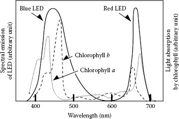
FIGURE 1.28 Photoemission spectra of red and blue LEDs and light absorption spectrum of chlorophyll. (From Okamoto, K. et al., Acta Hortic., 440, 111, 1996. With permission.)
1.4.7.6.2 Suppression of Mold’s Growth
During this research, Okamoto found also that blue LED light drastically suppresses the growth and propagation of blue mold, and on this basis, he developed a prototype of an anti-mold storage chamber, which is used for preserving food [145]. It consists of 2240 pieces of high-brightness blue (450 nm) LEDs. Blue mold spoils many foods and is normally treated with chemical agents. Inhibition of bluish mold propagation by 450 nm blue LED has important applications in the field of antibacteria and anti-mold technology, microbiology, food warehouses, antibacterial and antifungal facilities in hospitals, crops transportation facilities, etc.
1.4.7.6.3 Blue LED Fishing Lamp
Most marine species including squids show regular phototaxis—fish is attracted by light and proceed toward the light source. There is a logarithmic relationship between the catch and the light intensity, and therefore, squid fishing is done during the night using very powerful fishing lamps. A typical fishing lamp consists of 60 metal-halide bulbs, each with electric power consumption of 3 kW. Hence, the total electric power consumption of the fishing-lamp system exceeds 180 kW per ship. In the peak season (June and July), more than 10,000 squid fishing boats of Japan and South Korea work around the Sea of Japan and the Korean Strait. More than 90% of the squid-fishing boats are small vessels, under 10 tons, and less than 20 m in length, and such a ship consumes as much as 500–1000 L petroleum per night. The total energy consumption attains 1 GW, which can be compared to the electric capacity of an atomic power station, and results in emission of huge amounts of gases of significant environmental concern such as CO2, SO2, and NO2. The light from the fishing lamps is intolerably strong and dazzling, and in addition, contains intensive UV component that is harmful to fishermen and marine life. The development and the subsequent wide implementation in the squid-fishing of a new type, the LED fishing lamp [146,147], have drastically reduced many of the problems discussed above. The LED fishing lamp has many advantages over the conventional metal-halide fishing lamp: 30 times less energy consumption, high efficiency, long life, compact, and environment friendly. Another unquestionable advantage is the opportunity for underwater implementation of the LED fishing lamp [148].
The laser is a device that generates a highly collimated, high-intensity beam of monochromatic and coherent radiation. What distinguish lasers from the conventional light sources are the unique properties of laser light: coherence, monochromaticity, directionality, polarization, and high intensity. The most common lasers today can deliver continuous wave (cw) or pulsed power output with wavelengths that vary from 193 nm (deep UV) to 10.6 μm (far IR), with cw power outputs that vary from 0.1 mW to 20 kW, or pulses with duration as short as a few femtoseconds and pulse energies as high as 104 J, and whose overall efficiencies (laser energy out divided by pump energy in) vary from less than 0.1% to 20% [15]. Lasers are used in applications that require light with very specific properties, which cannot be provided by other light sources. Many high-precision techniques used in optical metrology, and described later in this book, employ phenomena and effects that originate from the unique properties of laser light. Therefore, we briefly review here some laser characteristics and parameters and some laser systems that are important for optical metrology. For a specific method, a laser system, or an application, the reader should refer to specialized books and the references thereafter describing in details the laser fundamentals, the different laser systems, and their area applications [149,150,151,152,153].
1.5.1 STIMULATED EMISSION AND LIGHT AMPLIFICATION
Light interact with matter via three processes, which provide thermodynamic equilibrium between light and matter: stimulated absorption (or simply absorption), spontaneous emission, and stimulated emission. Einstein showed that Planck’s empirical formula that describes blackbody radiation at thermodynamic equilibrium could be derived from the quantum theory of radiation only if all these three processes are considered.
Since the process of interaction of light with matter must conserve energy, only specific energy levels that are separated by the photon energy hν are involved in the absorption and emission of light. Absorption is the process by which light transfers energy to matter. For the absorption process, the principle of conservation of energy implies that an atom can absorb an incident photon of energy hν and undergo a transition from a lower energy state E1 to a higher energy state E2, only if E2 − E1 = hν. If the material is left undisturbed, the atom will eventually de-excite via a radiative or non-radiative transition to a lower energy state. If a radiative transition takes place, it will result in spontaneous emission of a photon, which has random phase and propagation direction. Stimulated emission occurs when an incident-stimulating photon of energy equal to the energy difference between the upper and the lower energy levels (hν =E2 − E1) interacts with the excited atom before spontaneous emission occurs. As a result, the atom de-excites via stimulated emission of a photon, which is an exact copy of the stimulating photon: it has the same frequency, phase, propagation direction, and polarization. In other words, both photons are spatially and temporally coherent.
The probability for absorption or stimulated emission process to occur depends on the photon energy density u(ν) in the frequency range driving the transition (measured in J s/m2). Spontaneous emission does not require a photon to occur; therefore, the corresponding probability is independent of the photon energy density u(ν). The rates of occurrence of these processes are given by the Einstein A21, B12, and B21 coefficients as follows: the probability of spontaneous emission of a photon is A21, the probability of absorption of a photon is the product B12u(ν), and the probability of stimulated emission of a photon is B21u(ν).
The number of atoms per unit volume that is in a given energy state defines the population density of that state. Let us denote the population densities of the lower E1 and higher E2 energy states with N1 and N2, respectively. The rate of change of the population of a given energy state or the transition rate depends on both the transition probability and the population of that state. Thus, the decay of the population N2 of the higher energy state E2 due to both the spontaneous and the stimulated emissions can be written as
The transition rate for absorption is
At thermodynamic equilibrium, the rate of emission must be equal to the rate of absorption (dN2/dt) = −(dN1/dt), thus
The population Ni of a higher energy state Ei is given by the Maxwell–Boltzmann distribution
where
N0 is a constant for a given temperature
T is the equilibrium temperature
kB is Boltzmann’s constant
The higher the energy state, the fewer atoms will be in that state. By substituting N1 and N2 in Equation 1.55 with Equation 1.56 for i = 1, 2 and using E2 − E1 = hν yield
Einstein was able to derive a relation between the coefficients , and B21 from the condition of thermodynamic equilibrium between a radiation field and an assembly of atoms. The quantum theory of blackbody radiation gives the following expression for the spectral energy density in an electromagnetic field in thermodynamic equilibrium with its surroundings at temperature T [15,154]:
Equation 1.57 can be reduced to Equation 1.58 only if the following relations between the Einstein coefficients hold:
and
This implies that as the energy density u(ν) becomes large, the rate of spontaneous emission becomes negligible, and the probability of stimulated emission is equal to the probability of stimulated absorption. The equality of the Einstein coefficients in Equation 1.59 leads to equality of the ratios of the rates for stimulated emission Rstim to that of absorption Rabs and the population density of the upper and lower energy levels, N2 and N1, respectively:
At thermodynamic equilibrium, the population N1 is much larger than N2. When E2 − E1 = 1 eV, N2/N1 is typically of the order of 10−17. This means that practically all the atoms are in the ground state, and the overall rate of absorption is always higher than the rate of stimulated emission. Therefore, absorption is always the dominant process for a collection of atoms in thermodynamic equilibrium; thus, light amplification cannot occur at equilibrium condition.
Amplification of radiation can take place only if population inversion is created and maintained in the atomic system, that is, the population of a higher energy level is kept larger than the population of a lower energy level. The probability for a photon with energy equal to the difference of the inverted levels to initiate stimulation emission is higher than the probability to be absorbed. As the stimulating and stimulated photons travel in the material, more stimulated emissions than absorptions will take place, and the number of photons will increase exponentially with the distance along the beam in the material. So will the irradiance of the beam, and as the beam has very high degree of directionality, this will be valid also for the beam intensity I(z):
where
I0 is the initial intensity of the radiation at z = 0
z is the distance along the beam direction
G (1/m) is the gain of the medium
The gain gives the number of photons created by stimulated emission per unit length of the traveled distance.
1.5.2 ESSENTIAL ELEMENTS OF A LASER
The first condition for amplification of light is the presence of a gain medium (also called active medium) capable of sustaining a preferential population inversion that leads to stimulated emission.
In order for an assembly of atoms to amplify an incident radiation, the atoms have to be driven out of thermal equilibrium and population inversion has to be created. This is possible only if energy from outside (pump energy) is supplied to the atomic system that selectively populates an excited state. A nonequilibrium condition cannot be reached and maintained simply by increasing the temperature of the system. Thus, the second condition for light amplification is the continuous supply of pump energy that creates and maintains a preferential population inversion leading to stimulated emission. Most laser materials have very low gain, typically between 0.01 and 0.0001 cm−1. In order to produce a large amplification, the light has to pass a long length of the laser medium. This can be achieved by placing the gain medium between two mirrors that bounce the light back and forth through the active medium. The gain medium and both mirrors form the resonant laser cavity.
The essential elements of a laser are the gain medium, the pump, and the laser cavity or resonator. Lasers with medium- and high-power outputs require also a cooling system.
The gain medium can be an assembly of atoms, ions, or molecules in a gas- (or plasma), liquid-, or solid-state phase. The gain medium of some solid-state lasers consists of a host and active atoms. For example, in the Nd:YAG laser, the YAG crystal is the host and the trivalent neodymium ions are the active element; in the ruby laser, the Al2O3 crystal is the host, and chromium ions Cr3+ (about 0.05%) are the active element. In order to produce laser emission, the gain medium must have proper set of energy states that can be effectively pumped to create population inversion and can serve as laser levels. The upper laser level should be a long-lived metastable state. A metastable state has typical lifetime of the order of 10−3 s, whereas most excited levels in an atom might decay in times of the order of 10−8 s. Figure 1.29 shows a four-level energy diagram. The excitation energy pumps electrons from the ground level to the excited state E3, which decays very rapidly to the metastable state E2 creating a population inversion. The laser emission can start with a spontaneously emitted photon via the transition E2 → E1, followed by an avalanche-stimulated emission; because of the long lifetime of the metastable state, the probability for stimulated emission is much higher than the probability for spontaneous emission. In general, laser emission can take place between the metastable state E2 and the ground state E0 (as in the case of the Ruby laser). Since the ground level has the largest population at thermodynamic equilibrium, a substantial pumping energy is required to create population inversion. In the four-level laser, however, the lower laser level is not the ground state. As soon as some electrons are pumped to the upper laser level E2, population inversion is achieved. This requires less pumping energy than does a three-level laser. In the four-level system, the lower laser level E1 is an ordinary level that depopulates rapidly by a relaxation process returning the atoms in the ground state. Thus, the population inversion is continuously maintained.
FIGURE 1.29 Four-level energy diagram.
The pump is a source of external energy that provides the required population inversion in the gain medium. The most commonly used pump mechanisms are optical pumping and electrical discharge (for gas lasers). Lasers with solid-state and liquid (dyes) gain media use optical pumping (by a flashlamp or another laser, most often diode lasers). Semiconductor lasers use electric current and optical pumping. Xenon and krypton lamps are most often used, because of their high efficiency of conversion of electrical input to light output, ≈60% and 50%, respectively. Krypton lamps serve for optical pumping of Nd:YAG lasers. All gas lasers use electric discharge, as all excimer lasers use short-pulse electric discharge. In monoatomic or monomolecular gas lasers, the free electrons generated in the discharge process collide with and excite the atoms, ions, or molecules directly. In a two-component gas mixture, the gases are chosen to have coinciding excited states and the excitation results from inelastic atom–atom (or molecule–molecule) collisions. This is the case of a He–Ne laser. Helium has an excited energy state that is 20.61 eV above the ground state, whereas neon has an excited state that is 20.66 eV above its ground state and just 0.05 eV above the first excited state of the helium. The free electrons generated in the gas discharge collide with and transfer energy to the helium atoms, which excite the neon atoms by collision and resonant transfer of energy. The kinetic energy of the helium atoms provides the extra 0.05 eV of energy needed to excite the neon atoms to the 20.66 eV metastable state.
The laser resonator converts the gain medium into an oscillator and hence into a light generator. The purpose of the laser cavity is threefold: (1) to confine the emission in the active medium, thus increasing the photon density and the probability for stimulated emission; (2) to enhance the amplification; and (3) to shape the beam. The laser cavity represents a Fabry–Perot resonator of two carefully aligned plane or curved mirrors [155,156]. A highly reflecting mirror (reflectivity as close to 100% as possible) serves as a back mirror, and a partially reflecting mirror (about 99%) is the output coupler, which allows a certain fraction of the laser light to escape the cavity and to form the external laser beam. The resonator provides the optical feedback by directing the photons back and forth through the active medium. The multiple passes ensure the amplification of the radiation in the direction of the beam, which accounts for the amazing degree of collimation of the laser beam. As the photon density in the cavity grows, the rate of stimulated emission increases causing a decrease of the population inversion in the gain medium. In addition, a fraction of the radiation exits through the output coupler at every round-trip and is lost for the cavity. The intensity of the light after a round-trip in the cavity can be expressed from Equation 1.62 as
where
L is the length of the laser medium within an optical cavity
R1 and R2 are the reflectances of the two mirrors
To maintain the amplification of the stimulated emission, it is required that
which leads to the condition for lasing:
Equation 1.65 is used in designing the laser cavity. The reflectance of the output mirror can be calculated for a given length of the active medium. Let us assume that the length of a laser tube is 150 mm and the gain factor of the laser material is 0.0005 cm−1. If R1 = 100%, the reflectance of the output coupler R2 as calculated using Equation 1.65 should be equal or higher than 98.5% in order to maintain the lasing.
The amount of stimulated emission grows on each pass until it reaches an equilibrium level. When the gain equals the losses per round-trip of the radiation through the cavity (condition of gain saturation), the laser settles into steady-state continuous wave operation.
The overall efficiency of a laser system is the ratio of the optical output power of the laser to the total power required to pump the laser. Typical efficiencies range from fractions of percent to about 25%, as for the most commonly used lasers they are below 2%. Carbon dioxide (CO2) lasers have efficiencies between 5% and 15%, dye lasers ~1% and 20%, whereas the most efficient are the semiconductor lasers ~1% and 50%. The losses are mainly thermal losses, and therefore, for high-power lasers the cooling is essential. Argon ion gas laser is one of the most commonly used lasers in realtime holography. The overall efficiency of a 10 W argon laser is 0.05%, and the total power used is 2 × 10⁴ W. Of this power, 99.95% is wasted as heat energy that if not removed, will damage the components of the system. Argon and krypton lasers use water cooling or forced air depending on the length of the tube and output power.
The cooling method depends mainly on the laser output power. The low-power HeNe, HeCd, and erbium:fiber lasers are air cooled and do not need external cooling. Gas lasers that produce medium- to high-level output powers, in particular, CO2 laser can reach up to 20 kW, are cooled by air, water, or forced air. The solid-state lasers use air or water cooling. The Nd:glass laser uses only water cooling, while semiconductor lasers are designed to work with air cooling and heat sink.
1.5.3 OPERATING CHARACTERISTICS OF A LASER
The stability of the Fabry–Perot cavity is determined by the radius of curvature and the separation between the mirrors. For a stable cavity, the radius of curvature should be several times the distance between the mirrors. Fabry–Perot cavity will support standing wave modes of wavelengths λm and frequencies νm that satisfy the condition
where
L is the separation of the mirrors
c is the speed of light in vacuum
n is the refractive index of the active medium
m is a large positive integer
The longitudinal cavity modes νm of oscillations (called also axial modes) correspond to standing waves set up along the cavity or z-axis. Consecutive modes are separated by a constant difference, which is the free spectral range of the Fabry–Perot etalon [155,156]:
In this equation, Δν also corresponds to the inverse of the round-trip time. Using dλ = (λ2/c)dν, the corresponding distance between two adjacent modes Δλ is expressed by
The gain of the laser medium is determined by the bandwidth of the spontaneous atomic transition and is also a function of the wavelength. As shown in Figure 1.30, the resonant modes of the cavity are much narrower than the gain profile. The actual wavelength content of the laser beam is the product of the envelope of longitudinal oscillation modes and the gain profile. Therefore, the cavity can select and amplify only certain modes, or even only one if desired. Hence, the resonator acts as a frequency filter, which explains the extreme quasi-monochromaticity of the laser light. For example, a typical He–Ne laser, λ = 632.8 nm and n = 1, has a cavity length of 30 cm, and the mode separation Δλmode is
FIGURE 1.30 Several resonant modes can fit within the gain profile.
Considering that the half-width of the gain profile of He and Ne gases is about 2 × 10⁻¹² m, three longitudinal modes can be excited.
As indicated by the example above, several wavelengths satisfy the oscillation condition. The coexistence of multiple modes reduces the monochromaticity of the laser light and should be avoided in many applications. One possible way to generate a single mode in the cavity would be to decrease the length of the cavity (see Equation 1.68) in order to make the mode separation exceed the transition band. However, this limits the length of the amplifying medium and thus the output power of the laser. The most common technique is to insert a Fabry–Perot etalon, a pair of reflective surfaces, between the laser mirrors to form a second resonant cavity. Of the multiple longitudinal modes of the laser cavity, only the one that coincides with the etalon mode will continue to oscillate; all other modes will be canceled by destructive interference when they pass through the etalon.
The cavity can sustain also transverse modes, which determine the transverse irradiance pattern of the beam corresponding to the distribution of the electromagnetic field within the laser cavity. While the longitudinal modes are governed by the axial dimensions of the resonant cavity, the transverse modes are determined by the cross-sectional dimensions of the laser cavity. The last depends on the construction of the resonator cavity and the mirror surfaces. The transverse modes are denoted as TEMmn (from transverse electric and magnetic) modes, where n and m are integers, which give the number of nodes in the x- and y-direction across the emerging beam. The larger the values of m and n, the more bright spots are contained in the laser beam.
The lowest order transverse mode or the fundamental mode TEM00 represents a Gaussian beam and has special characteristics, because of which lasers operating in a single TEM00 mode are widely used in high-precision measurement systems: a Gaussian beam is completely spatially coherent, provides the smallest beam divergence, and can be focused down to the smallest-sized spot, limited only by diffraction and lens aberrations. Most laser cavities are designed to produce only the TEM00 mode. This can be achieved by placing a small circular aperture that is slightly larger than the spot size of the TEM00 mode in the middle of the laser cavity. Alternatively, by making the bore diameter of the laser tube just slightly larger than the spot size of the TEM00 mode. However, lasers that are designed to maximize the output power operate in higher order modes.
The distribution of the irradiance across a Gaussian beam is described by a Gaussian function, a bell-shaped curve that is symmetrical around the central axis:
where
r is the radial distance measured from the central axis
I0 is the irradiance at the center of the profile
At r = w, Equation 1.69 becomes I = I0e−2 = 0.14I0, and the beam irradiance is only 14% of the maximum value I0.
In order for the laser cavity to be stable or marginally stable, one or both mirrors have to be curved. The curved mirrors tend to focus the beam. As a result, the cross section of the beam changes along the optical axis of the cavity and reaches a minimum value somewhere between the mirrors. The smallest beam cross section is called beam waist. The radius of the beam waist w0 is usually given in the technical data sheet of the commercial lasers. The radius and exact location of the beam waist are determined by the design of the laser cavity and depend on the radii of curvature of the two mirrors and the distance between the mirrors. For example, the beam waist in a confocal resonator is halfway between the mirrors. (A confocal resonator is a marginally stable resonator with radius of curvature of both mirrors equal to the spacing between the mirrors.) The size of the beam waist determines the external divergence of the laser beam, which is a continuation of the beam divergence out from this waist. The half-width of the beam at any point along the z-axis can be derived from a rigorous analysis of the electromagnetic field in the cavity, when the beginning of the coordinate system z = 0 is set at the beam waist and is given by [157]
Besides the beam waist, the Rayleigh range zR is another important characteristic of a Gaussian beam. It is defined as
At z = zR, Equation 1.71 yields . Hence, the Rayleigh range is the distance at which the cross-sectional area of the Gaussian beam doubles. In addition, the Rayleigh range is the distance at which the curvature of the beam wavefront is minimum. As the beam propagates along z, the curvature of the beam wavefront varies with z according to
At the beam waist, z = 0 and R(0) → ∞, and the wavefronts are plane. Within the Rayleigh range |z| < zR, the beam remains collimated. At z = zR, the curvature of the beam wavefront has the smallest value R(zR) = 2zR. The far-field beam divergence is determined by the full-angular width via the relation
Equation 1.73 shows that the far-field divergence of a Gaussian beam is inversely proportional to the beam waist w0; the smaller the beam waist w0 is, the smaller the Rayleigh range (see Equation 1.71), and the faster the beam diverges.
If the cavity consists of plane mirrors, the beam will be aperture limited via diffraction. The divergence of an aperture limited circular laser beam of diameter D is
1.5.3.3 Continuous Wave and Pulsed Operation
A laser can operate in cw or in pulsed mode. A laser in cw mode delivers a beam of constant irradiance, whereas in pulsed mode, a laser can deliver pulses with durations as small as a few femtoseconds. The laser output can be pulsed by different methods, as the most commonly used are the Q-switching and mode locking [149]. He–Ne and He–Cd lasers deliver only cw output, while the nitrogen, Nd:glass, and excimer gas lasers deliver only pulsed output. Argon and krypton lasers can operate in cw or in pulsed modes achieved by mode locking of the cw output. The following lasers can also be operated in both cw and pulsed modes: CO2 (long pulse), dye (ultrashort pulse), Nd:YAG, Ti:sapphire (ultrashort pulse), alexandrite and erbium:fiber, and all semiconductor lasers. The pulsed output allows controlling the laser energy delivery in material processing applications. Pulsed lasers are used also in time-resolved spectroscopy, holography of moving objects, in time-of-flight distance measurements, and other applications.
1.5.4 CHARACTERISTICS OF LASER LIGHT
In general, the degree of monochromaticity of a light source is defined by the linewidth Δν, which is the FWHM of the spectral emission of the source. The spectral bandwidth Δλ, which is found by interference theory [157], is given by
where R is the reflectance of the output mirror.
The laser output results primarily from stimulated emission of photons with identical frequencies. However, some spontaneously emitted photons with random phase can also contribute to the laser output; thus, causing the finite linewidth of the laser emission. Besides this inherent effect, other external factors such as mechanical vibrations, which change the cavity length, or variations of the index of refraction of the gain medium additionally broaden the linewidth of a laser. Nevertheless, the lasers provide the highest degree of monochromaticity, almost reaching the ideal limit. For instance, the spectral bandwidth of the ruby laser is only Δλ = 0.53 nm (λ = 694.3 nm). The reason for the high degree of laser light monochromaticity is the additional frequency-filtering effect of the Fabry–Perot laser cavity.
Coherence is the most prominent characteristic of laser light. The degree of coherence is determined by the degree of correlation between the phases of the electromagnetic field at different locations (spatial coherence) and different times (temporal coherence). Temporal coherence is a measure of the degree of monochromaticity of the light, whereas spatial coherence is a measure of the uniformity of phase across the optical wavefront. An ideal monochromatic point source, illustrated in Figure 1.31, produces perfectly coherent light. As the point source emits an ideal sinusoidal wave, it is easy to predict the phase of the radiation at a given point at a given time t2, if we know what was the phase at the same point at an earlier time t1. This is perfect temporal coherence. The longitudinal spatial coherence requires correlation between the phases in a given moment at two points P1 and P2 located along a radius line and is similar to temporal coherence. Therefore, the temporal coherence is also called longitudinal spatial coherence. Now, let us consider two points P1 and P3 along the same wavefront. Perfect transverse spatial coherence means that if we know the phase of the wave at point P1 at time t1, we can predict the phase of the field at this same moment at point P3 along the same wavefront.
A conventional light source, such as a tungsten lamp, produces incoherent light. In order to obtain partially coherent light from a tungsten lamp, a filter and a pinhole have to be used, but this reduces drastically the light intensity. In the laser active medium, neighboring point sources produce light of the same frequency and with correlated phase. Thus, the high degree of temporal and spatial coherences of laser light is an inherent property originating from the process of generation of laser light via stimulated emission. A single-mode laser beam exhibits the highest degree of temporal and spatial coherences, as the transverse spatial coherence extends across the full width of the beam.
1.5.4.2.1 Temporal Coherence
The temporal coherence is determined by the natural linewidth Δν of the emitted radiation, and thus is a manifestation of spectral purity. The radiative electron transitions that result in spontaneous emission of photons have finite durations on the order of 10−8 to 10−9 s. This is the time extent during which a single-photon wavetrain will be nicely sinusoidal. Because the emitted wavetrains are finite, there will be a spread in the frequencies, which determine the natural linewidth Δν of the emitted radiation. The coherence time tc is the same order of magnitude as the reciprocal of the natural linewidth Δν.
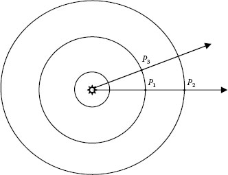
FIGURE 1.31 Monochromatic point source emits perfectly coherent light.
The coherence time tc is determined by the average time interval over which the phase of the wave at a given point in the space can be reliably predicted. The coherence length lc is the spatial extend over which the phase of the wave remains unchanged, or it is simply the distance traveled by the light within the coherence time:
where c is the speed of light in vacuum. The coherence length depends on the nominal wavelength and the spectral bandwidth of the laser beam, as given by
The coherence length is a very useful measure of temporal coherence, because it tells us how far apart two points along the light beam can be and still remain coherent with each other. In interferometry and holography, the coherence length is the maximum optical path difference that can be tolerated between the two interfering beams.
The broad continuous spectrum of white light has a bandwidth about 0.3 × 10¹⁵ Hz, the coherence time is roughly 3 × 10⁻¹⁵ s, and the coherence length is only few wavelengths long. The narrow emission line from a low-pressure mercury lamp (λ = 546 nm) is an example of quasi-monochromatic light; it has a linewidth of about 109 Hz, which corresponds to coherence time of about 1 ns, and coherence length of approximately 0.3 m. Typically, frequency-stabilized lasers with long laser cavities have coherence lengths that can be several meters. For a single-mode He–Ne laser, the coherence time is of the order of microsecond and the coherence length is hundreds of meters.
A high degree of coherence is essential for interferometry and holography, which are the foundations of a large group of optical metrology techniques for noninvasive and nondestructive testing. The coherence length of a monochromatic light source can be measured easily using a Michelson interferometer [155,156]. One of the mirrors is mounted on a translation stage, so that the optical path difference ΔL between the two beams in the arms of the interferometer can be varied. Whenever the optical path difference ΔL is equal to an integer number of wavelengths, the two beams interfere constructively resulting in a bright central spot. (Circular fringes will be observed only if the optical surfaces of the mirrors constructing the interferometer are perfectly flat; imperfect surfaces result in distorted fringe pattern.) The visibility V of the fringe pattern is determined by the maximum and minimum intensities, Imax and Imin, of the bright and dark fringes, respectively:
As ΔL increases, the visibility V of the fringe pattern begins to decrease. The coherence length lc is defined as the value of the optical path difference ΔL at which the visibility of the fringes is one half. This way, the fringe visibility can be used as a measure of coherence: V = 1 corresponds to complete coherence, while V = 0 indicates lack of any coherence or complete incoherence. If 0 < V < 1, there is partial coherence.
1.5.4.2.2 Transverse Spatial Coherence
The Van Cittert–Zernike theorem [158] defines the area of spatial (or lateral) coherence within the central maximum of the Fraunhofer diffraction of a circular aperture. If an extended light source is considered as an aperture of the same size and shape, the central maximum of the diffraction pattern produced by this aperture will correspond to the region of coherence of the extended light source. According to the Van Cittert–Zernike theorem, a thermal source such as a star with an angular diameter θ produces a region of spatial coherence with width ls given by
where θ is measured in radians.
The classical double-slit experiment of Young can be used for demonstration of the transverse spatial coherence. The two slits act as two point sources of quasi-monochromatic light with wavelength λ separated by a distance d. The light waves from the two slits interfere constructively and destructively to produce bright and dark fringes observed on a screen. The interference pattern on the screen will consist of stationary fringes only when the light exiting the slits is correlated in phase. At the location of zero path difference, the constructive interference results in a bright fringe. The area of constructive interference, that is, the central bright fringe, defines the region of spatial coherence. The spacing of the interference fringes depends on the double-slit separation d, whereas their visibility depends on the spatial coherence width ls. As ls approaches the limit specified by Equation 1.80, the visibility decreases to zero and the fringes disappear when Equation 1.80 is satisfied.
When Young’s experiment uses white light, the central fringe of the resultant interference pattern is white, and the fringes on both sides of it are rainbows of colors. All frequencies from the white spectrum have zero optical path difference in the area of the central fringe; they interfere constructively there and form the white fringe. This shows that even white light and light from thermal sources that emit a broad spectrum exhibit some degree of spatial coherence. For example, the spatial coherence width for Sun is ls = 0.0768 mm, as calculated with Equation 1.80 when assuming a circular cross section with angular diameter θ ≈ 0.5° and average wavelength of 550 nm. Sun is an extended thermal source, and it illuminates a properly oriented observing screen uniformly. However, if two tiny apertures are placed at a distance less than ls = 0.0768 mm, they will produce interference fringes. To see interference fringes from an extended source with more widely spaced apertures, the light from the source has to pass through a single small aperture initially in order to create an area of coherence that is large enough to contain the two-slit aperture.
A manifestation of high degree of coherence is the laser speckle effect that can be easily observed when a laser beam is diffusely reflected from a rough surface such as painted wall. The coherent laser light is scattered from the surface granules, which act as small point sources of coherent wavelets that combine and produce a stationary interference pattern in the surrounding space and are projected on the retina of the eye. Speckle is not observed if the same surface is illuminated with natural light. This is because the coherence length of natural white is much less than the optical path difference between two wavelets scattered from different surface bumps and arriving at a given point in the space. The speckle effect will be presented in more details in Chapter 4.
No other light source can provide a beam with such a degree of collimation like the laser. The high directionality of the laser beam originates from the geometrical design of the laser cavity and of the fact that the stimulated emission process produces identical photons propagating in the same direction. A single-mode laser beam exhibits smaller divergence than a multimode beam. The divergence angle of a single-mode (TEM00) laser output is given by Equation 1.73. The smaller the beam waist w0, the larger the divergence angle. For a He–Ne laser (632.8 nm) with an internal beam waist of radius about 0.25 mm, the divergence angle of the beam is 8 × 10⁻⁴ rad. Typical values for the beam divergence of the He–Ne lasers are 0.5–3 mrad. Argon and krypton ion gas lasers and various dye lasers exhibit the lowest divergence of 0.4–1.5 and 0.3–2 mrad, respectively, while the semiconductor lasers have an oval beam with the largest divergence 200–600 mrad. The beam divergence of molecular gas lasers is 1–7 mrad, the excimer gas lasers have divergence of 2–6 mrad, and for solid-state lasers it varies up to 25 mrad.
Conventional light sources have finite dimensions and emit strongly divergent light. Therefore, the image of a lightbulb, for instance, formed by a lens (or a mirror) has a finite size, and only the light that is intercepted by the lens contributes to the image irradiance, as most of the light output of the bulb is lost. A laser beam, in contrast, has a small diameter and is highly collimated. Thus, a lens can focus all the laser power in a spot on the order of the laser wavelength, as the spot’s size is limited only by lens aberrations and diffraction. This way, a very high energy density can be achieved in a very small spot, and can be used for laser-material processing (drilling, cutting, material removal, melting, welding, etc.) in many industrial applications, as well as in surgery or other medical applications.
Due to both small divergence and small diameter of the laser beam, the irradiance (power per unit area) of a laser is far greater than the conventional light sources. Let us compare the irradiance of a He–Ne laser with an output power of 1 mW and a lightbulb with output power of 100 W. Because of the small divergence of the laser beam, the beam radius is still about 2 mm at a distance 1 m from the laser, and the irradiance would be
The lightbulb, though, emits in all directions, so the illuminated area is a sphere with an area 4πr2. The irradiance 1 m from the 100 W lightbulb would be
Hence, the irradiance 1 m from the lightbulb is a factor of 10 times smaller at 105 times larger output power compared with the He–Ne laser.
In general, lasers are classified by the type of the active media. The most commonly used lasers today are listed below their main emission wavelengths, output power, and mode of operation given in parentheses [15].
• Atomic gas lasers include the He–Ne laser (λ = 632.8 nm, etc.; 0.1–50 mW; and cw) and the He–Cd laser (λ = 325, 441.6 nm, etc.; 5–150 mW; and cw).
• Ion gas lasers include the argon laser (main lines at λ = 488 and 514.5 nm, and others from 350 to 530 nm; 2 mW to 20 W; and cw or mode-locked) and the krypton laser (λ = 647.1 nm and others from 350 to 800 nm; 5 mW to 6 W; cw or mode-locked).
• Molecular gas lasers include the carbon dioxide laser (λ = 10.6 μm, 3 W–20 kW, and cw or long pulse) and the nitrogen laser (λ = 337.1 nm).
• Excimer gas lasers include the argon fluoride (λ = 193 nm and up to 50 W average), the krypton fluoride (λ = 248 nm and up to 100 W average), the xenon chloride (λ = 308 nm, etc.; and up to 150 W average), and the xenon fluoride (λ = 351 nm, etc.; and up to 30 W average), all in pulsed output.
In general, gas lasers have better coherence characteristics and are cheaper than other types of lasers. The He–Ne laser is the most economical choice for measurement and control applications based on low-power cw laser output. It operates on a single line at 632.8 nm and the output can be strongly polarized. In addition, it does not require external cooling system; it is very simple to operate and has a long life. However, commercial He–Ne lasers oscillate in two to five longitudinal modes, depending on the power and have limited coherence length. Argon and krypton ion lasers deliver high-power output with extended coherence length. A single line can be selected from the multiline output of the Ar+ or Kr+ lasers, if the end mirror of the laser cavity is replaced by a prism, while a single longitudinal mode can be isolated by incorporating a Fabry–Perot etalon in the cavity.
The group of liquid lasers consists of various dye lasers (tunable λ = 300–1000 nm, 20 mW–1 W average, and cw or ultrashort pulsed). With a given dye, the operating wavelength can be tuned within a range of 50–80 nm by a wavelength selector, such as a diffraction grating or birefringent filter, incorporated in the cavity. Changing the wavelength over a wide range is obtained by switching dyes.
1.5.5.3 Solid-State Active Medium
The group of solid-state lasers include the Nd:YAG laser (λ = 1.064 μm, up to 10 kW average, and cw or pulsed), the Nd:glass laser (λ = 1.06 μm), Ti-sapphire laser (tunable λ = 660–1000 nm, ~2 W average power, and cw or ultrashort pulsed), and the erbium:fiber laser (λ = 1.55 μm, 1–100 W, and cw or pulsed). A Nd:YAG laser is pumped optically with flashlamp, arc lamp, or diode laser. The advantage of using a diode laser to pump a Nd:YAG with a frequency doubling crystal is that such a system is more compact and lighter. In addition, it delivers a cw output of green light (λ = 532 nm) with a coherence length of few meters and output power up to 100 mW. The ruby laser (λ = 694.3 nm) was the first laser. It is pumped by a flashlamp with pulse durations ranging from a fraction of a millisecond to a few milliseconds. It delivers output with pulse energy up to 100 J/pulse. It can operate in single mode or multimode and can also be Q-switched. The ruby laser is still the most widely used pulsed laser for optical holography, because of the large output energy and the match of the laser wavelength to the peak sensitivity of commercial photographic materials for holography [159].
1.5.5.4 Semiconductor Active Medium
Although semiconductor lasers employ solid-state media, they are usually presented in a separate group because of their specific construction, operation, and properties. Typical representatives of this group of lasers are GaAs and GaAlAs (both emitting at λ = 780–900 nm and 1 mW to several watts), and InGaAsP lasers (λ = 1100–1600 nm and 1 mW to ~1 W). They operate on the principle of edge-emitting LEDs and surface-emitting LEDs, with the main difference that the semiconductor lasers have polished ends or use the cleaved surfaces at the ends of the laser crystal, providing optical feedback, thus a laser cavity. The semiconductor lasers operate with relatively low power input and are very efficient. They are very small, diffraction limited point source, and therefore do not require a spatial filter. They can be made to operate in a single longitudinal mode and deliver cw or pulsed output. The emission wavelength range depends on the alloy composition. The main disadvantage of this group of lasers is the large beam divergence in comparison with the other types of lasers.
The choice of a laser depends on the specific application. Most of the optical metrology techniques employ lasers with light output in the visible range such as He–Ne, He–Cd (441.6 μm), Ar3+, Kr3+, tunable dye, Ti:sapphire, and alexandrite (both in the deep red range) lasers. Techniques that are based on interferometry and holography can employ pulsed lasers in order to eliminate problems connected with the stability of the recording system. Optical sensing and communication applications involving fibers use mainly the Nd:YAG laser. The most powerful CO2 laser is widely used in industrial applications such as material processing (laser cutting, welding, drilling, etc.), and almost all of the lasers presented above find applications in different medical procedures. The list of laser applications involving interaction of laser light with matter and laser processing of information is very long and diverse and is out of the scope of this text. The reader can find abundant information in books devoted on laser applications [149,159,160,161,162].
1. Boyd, R.W., Radiometry and Detection of Radiation, Wiley, New York, 1983.
2. DeCusatis, C., Handbook of Applied Photometry, American Institute of Physics (AIP) Press, Springer Verlag, New York, 1997.
3. Rea, M. (Ed.), Lighting Handbook: Reference and Application, 8th edn., Illuminating Engineering Society of North America (IESNA), New York, 1993.
4. International Commission on Illumination (CIE), The Basis of Physical Photometry, Publication No. 18.2, Technical Report, Paris, France, 1983.
5. Žukauskas, A., Shur, M.S., and Gaska, R., Introduction to Solid-State Lighting, John Wiley & Sons, Inc., New York, 2002, Chapter 2.
6. American National Standard Nomenclature and Definitions for Illuminating Engineering, ANSI Standard ANSI/IESNA RP-16 96, 1996.
7. The International System of Units (SI), 8th edn., International Bureau of Weights & Measures (BIPM), STEDI Media, Paris, France, 2006.
8. Cromer, C.L. et al., The NIST detector-based luminous intensity scale, Journal of Research of the National Institute of Standards and Technology, 101, 109, 1996.
9. Bergh, A.A. and Dean, P.J., Light-Emitting Diodes, Clarendon Press, Oxford, U.K., 1976.
10. Gillessen, K. and Schaiper, W., Light-Emitting Diodes: An Introduction, Prentice Hall, Englewood Cliffs, NJ, 1987.
11. Stringfellow, G.B. and Craford, M.G. (Eds.), High Brightness Light Emitting Diodes, Semiconductors and Semimetals, Vol. 48, Series Eds. R.K. Willardson and E.R. Weber, Academic Press, San Diego, CA, 1997.
12. Schubert, E.F., Light-Emitting Diodes, Cambridge University Press, Cambridge, U.K., 2003.
13. MacAdam, D.L. (Ed.), Colorimetry—Fundamentals, SPIE Optical Engineering Press, Bellingham, WA, 1993.
14. Wyszecki, G. and Stiles, W.S., Color Science: Concepts and Methods, Quantitative Data and Formulae, Wiley, New York, 2000.
15. Pedrotti, F.L., Pedrotti, L.S., and Pedrotti L.M., Introduction to Optics, 3rd edn., Pearson Prentice Hall, Upper Saddle River, NJ, 2007, p. 421.
16. Judd, D.B., Report of U.S. Secretariat Committee on colorimetry and artificial daylight, Proceedings of the 12th Session of the CIE, Bureau Central de la CIE, Stockholm, Paris, Vol. 1, 1951, p. 11.
17. Vos, J.J., Colorimetric and photometric properties of a 2-deg fundamental observer, Color Research and Application, 3, 125–128, 1978.
18. Brindley, G.S., The color of light of very long wavelength, Journal of Physiology, 130, 35–44, 1955.
19. CIE, Commission Internationale de l’Eclairage Proceedings, 1931, Cambridge University Press, Cambridge, U.K., 1932.
20. Stiles, W.S. and Burch, J.M., Interim report to the Commission Internationale de l’Éclairage Zurich, 1955, on the National Physical Laboratory’s investigation of colour-matching, Optica Acta, 2, 168–181, 1955.
21. Palmer, J.M., Radiometry and photometry: Units and conversions, in Handbook of Optics, 2nd edn., Part III, Ed. M. Bass, McGraw-Hill, New York, 2001.
22. Möller, K.D., Optics, University Science Books, Mill Valley, CA, 1988, p. 384.
23. Hodapp, M.V., Application of high-brightness light-emitting diodes, High Brightness Light Emitting Diodes, Eds. G.B. Stringfellow and M.G. Craford, Semiconductors and Semimetals, Vol. 48, Series Eds. R.K. Willardson and E.R. Weber, Academic Press, New York, 1997.
24. Rea, M.S. (Ed.), The IESNA Lighting Handbook, IESNA, New York, 2000.
25. Coaton, J.R. and Marsden, A.M. (Eds.), Lamps and Lighting, Arnold, London, U.K., 1997, p. 546.
26. Schmid, W. et al., High-efficiency red and infrared light-emitting diodes using radial outcoupling taper, IEEE Journal of Selected Topics in Quantum Electronics, 8, 256, 2002.
27. Johnson, H.L. and Morgan, W.W., Fundamental stellar photometry for standards of spectral type on the revised system of the Yerkes spectral atlas, The Astrophysical Journal, 117, 313–352, 1953.
28. Cousins, A.W.J., Revised Zero Points and UBV photometry of stars in the Harvard E and F regions, Monthly Notices of the Royal Astronomical Society, 166, 711, 1974.
29. Cousins, A.W.J., Standard stars for VRI photometry with S25 response photocathodes, Monthly Notes of the Astronomical Society of Southern Africa, 33, 149, 1974.
30. Landolt, A.U., UBVRI photometric standard stars in the magnitude range 11.5 < V < 16.0 around the celestial equator, The Astrophysical Journal, 104, 340, 1992.
31. Landolt, A.U., Broadband UBVRI photometry of the Baldwin-Stone southern hemisphere spectrophotometric standards, The Astrophysical Journal, 104, 372, 1992.
32. Kutner, M.L., Astronomy: A Physical Perspective, Harper & Row Publishers, New York, 1987, Chapter 18.
33. Baum, W.A., in Problems of Extra-Galactic Research, Ed. G.C. McVittie, IAU Symposium No. 15, Mac Millan Press, New York, 1962, p. 390.
34. Bolzonella, M., Miralles, J.-M., and Pelló, R., Photometric redshifts based on standard SED fitting procedures, Astronomy and Astrophysics, 363, 476–492, 2000.
35. Eccles, M.J., Sim, M.E., and Tritton, K.P., Low Light Level Detectors in Astronomy, Cambridge University Press, Cambridge, U.K., 1983.
36. Hall, D.S., Genet, R.M., and Thurston, B.L., Automatic Photoelectric Telescopes, The Fairborn Press, Mesa, AZ, 1986.
37. Henden, A.A. and Kaitchuk, R.H., Astronomical Photometry, Van Nostrand Reinhold Company, Inc., New York, 1982.
38. Wolpert, R.C. and Genet, R.M., Advances in Photoelectric Photometry, Vol. 1, Fairborn Observatory, Patagonia, AZ, 1983.
39. Golay, M., Introduction to Astronomical Photometry, Reidel Publishing Company, Boston, MA, 1974.
40. Low, F. and Rieke, G.H., The instrumentation and techniques of infrared photometry, Methods of Experimental Physics, 12, 415, 1974.
41. Robinson, L.J., The frigid world of IRAS—I, Sky and Telescope, 69(1), 4, 1984.
42. Schorn, R.A., The frigid world of IRAS—II, Sky and Telescope, 69(2), 119, 1984.
43. CIE Publication No. 15.2, Colour and Vision, Colorimetry, 2nd edn., 1986.
44. Ohno, Y., CIE fundamentals for color measurements, Proceedings of the IS&T NIP16 Conference, Vancouver, CA, October 16–20, 2000.
45. CIE Publication No. 13.3, Method of Measuring and Specifying Colour Rendering Properties of Light Sources, 1995.
46. Ohno, Y., Photometry and standards, OSA/AIP Handbook of Applied Photometry, Optical Society of America, Washington DC, 1997, Chapter 3, pp. 55–99.
47. ISO/CIE 10526–1991, CIE standard colorimetric illuminants, 1991.
48. ISO/CIE 10527–1991, CIE standard colorimetric observers, 1991.
49. Walker, J. et al., Spectral irradiance calibrations, NIST Special Publication, 250–20, National Institute of Standards and Technology, Gaithersburg, MD, 1987.
50. CIE Publication No. 17.4/IEC Publication 50(845), International Lighting Vocabulary, 1987.
51. Gray, D.F., The inferred color index of the Sun, Publications of the Astronomical Society of the Pacific, 104(681), 1035–1038, 1992.
52. The Simbad Astronomical Database Rigel page, http://simbad.u-strasbg.fr/simbad/sim-basic?Ident=Rigel&submit=SIMBAD+search.
53. Bessell, M.S., Publications of the Astronomical Society of the Pacific, 102, 1181, 1990.
54. Williams, E.W. and Hall, R., Luminescence and the Light Emitting Diode, Pergamon Press, New York, 1978, p. 241.
55. Weber, M.J. (Ed.), Selected Papers on Phosphors, Light Emitting Diodes, and Scintillators: Applications of Photoluminescence, Cathodoluminescence, Electroluminescence, and Radioluminescence, Milestone Series, Vol. 151, SPIE Optical Engineering Press, Bellingham, WA, 1998.
56. Lakowicz, J.R., Principles of Fluorescence Spectroscopy, 3rd edn., Springer, New York, 2006.
57. Masters, B.R., Selected Papers on Multiphoton Excitation Microscopy, Milestone Series, Vol. 175, SPIE Optical Engineering Press, Bellingham, WA, 2003.
58. Saleh, B.E.A. and Teich, M.C., Fundamentals of Photonics, 2nd edn., John Wiley & Sons, Inc., Hoboken, NJ, 2007.
59. Fox, M., Quantum Optics: An Introduction, Oxford University Press, New York, 2006.
60. Klauder, J.R. and Sudarshan, E.C.G., Fundamentals of Quantum Optics, Benjamin, Inc., New York, 1968; Dover Publications, Inc., Mineola, New York, reissued 2006.
61. Louisell, W.H., Quantum Statistical Properties of Radiation, John Wiley & Sons, Inc., Hoboken, NJ, 1973; reprinted 1990.
62. Saleh, B., Photoelectron Statistics, Springer-Verlag, New York, 1978.
63. Ullrich, B. et al., The influence of self-absorption on the photoluminescence of thin film CdS demonstrated by two-photon absorption, Optics Express, 9(3), 116–120, 2001.
64. Ullrich, B., Munshi, S.R., and Brown, G.J., Photoluminescence analysis of p-doped GaAs using the Roosbroeck-Shockley relation, Semiconductor Science and Technology, 22, 1174–1177, 2007.
65. Mueller, G. (Ed.), Electroluminescence I, Semiconductors and Semimetals, Vol. 64, Series Eds. R.K. Willardson and E.R. Weber, Academic Press, New York, 2000.
66. Mueller, G. (Ed.), Electroluminescence II, Semiconductors and Semimetals, Vol. 65, Series Eds. R.K. Willardson and E.R. Weber, Academic Press, New York, 2000.
67. Yacobi, B.G. and Holt, D.B., Cathodoluminescence Microscopy of Inorganic Solids, Plenum, New York, 1990.
68. Norman, C.E., Reaching the spatial resolution limits of SEM-based CL and EBIC, Microscopy and Analysis, 16(2), 9–12, Cambridge, U.K., 2002.
69. Galloway, S.A., Miller, P., Thomas, P., and Harmon, R., Advances in cathodoluminescence characterisation of compound semiconductors with spectrum imaging, Physica Status Solidi (C), 0(3), 1028–1032, 2003.
70. Parish, C.M. and Russell, P.E., Scanning cathodoluminescence microscopy, in Advances in Imaging and Electron Physics, Vol. 147, Ed. P.W. Hawkes, Academic Press, San Diego, CA, 2007, p. 1.
71. Frenzel, H. and Schultes, H., Luminescenz in ultraschallbeschickten Wasser, Zeitschrift für Physikalische Chemie, B27, 421, 1934.
72. Young, F.R., Sonoluminescence, CRC Press, Boca Raton, FL, 2005.
73. Gaitan, D.F. et al., Sonoluminescence and bubble dynamics for a single, stable, cavitation bubble, Journal of the Acoustical Society of America, 91, 3166, 1992.
74. Putterman, S.J., Sonoluminescence: Sound into light, Scientific American, 272(2), 46–51, 1995.
75. Matula, T.J. and Crum, L.A., Evidence for gas exchange in single-bubble sonoluminescence, Physical Review Letters, 80, 865–868, 1998.
76. Brenner, M., Hilgenfeldt, S., and Lohse, D., Single bubble sonoluminescence, Reviews of Modern Physics, 74, 425, 2002.
77. Taleyarkhan, R.P. et al., Evidence for nuclear emissions during acoustic cavitation, Science, 295, 1868, 2002.
78. Rauhut, M.M., Chemiluminescence, in Kirk-Othmer Concise Encyclopedia of Chemical Technology, 3rd edn., Ed. M. Grayson, John Wiley & Sons, New York, 1985, p. 247.
79. Barnett, N.W. et al., New light from an old reagent: Chemiluminescence from the reaction of potassium permanganate with sodium borohydride, Australian Journal of Chemical Education, 65, 29–31, 2005.
80. Bollyky, L.J. and Rauhut, M.M., American Cyanamid, U.S. Patent No. 3,597,362, Generation of light by the reaction of esters of oxalic-type acids, 1971.
81. Tsuji, A. et al. (Eds.), Bioluminescence and chemiluminescence: Progress and perspectives, Proceedings of the 13th International Symposium, World Scientific Publishing Co., Singapore, 2005.
82. Sweeting, L.M. et al., Crystal structure and triboluminescence II. 9-Anthracencecarboxylic acid and its esters, Chemistry of Materials (ACS), 9, 1103–1115, 1997.
83. Wheelon, A.D., Electromagnetic Scintillation, Cambridge University Press, Cambridge, U.K., 2001.
84. Tsai, K.B., Developments for a new spectral irradiance scale at the national institute of standards and technology, Journal of Research of the National Institute of Standards and Technology, 102, 551–558, 1997.
85. Waymouth, J.F., Electric Discharge Lamps, The MIT Press, Cambridge, MA, 1971.
86. Elenbaas, W., The High Pressure Mercury Vapor Discharge, North Holland Publishing Co., Amsterdam, the Netherlands, 1951.
87. Pankove, J.I., Optical Processes in Semiconductors, Dover Publications, Inc., New York, 1971.
88. Kasap, S.O., Principles of Electronic Materials and Devices, 2nd edn., McGraw Hill, New York, 2002.
89. Schubert, E.F. and Hunt, N.E.J., 15,000 hours stable operation of resonant-cavity light-emitting diodes, Applied Physics A, 66, 319, 1998.
90. Grundmann, M., The Physics of Semiconductors, Springer-Verlag, Berlin, Germany, 2006.
91. Craford M.G. et al., Radiative recombination mechanism in GaAsP diodes with and without nitrogen doping, Journal of Applied Physics, 43, 4075, 1972.
92. Groves, W.O., Herzog, A.H., and Craford, M.G., GaAsP electroluminescent device doped with isoelectronic impurities, US Patent Re. 29,845, 1978.
93. Holonyak, N., Jr. et al., The “direct-indirect” transition in Ga(AsP) p−n junctions, Applied Physics Letters, 3, 47, 1963.
94. Logan, R.A., White H.G., and Wiegmann W., Efficient green electroluminescent junctions in GaP, Solid State Electronics, 14, 55, 1971.
95. Steranka, F.M., AlGaAs red light-emitting diodes, in High Brightness Light Emitting Diodes, Eds. G.B. Stringfellow and M.G. Craford, Semiconductors and Semimetals, Vol. 48, Academic Press, San Diego, CA, 1997.
96. Ishiguro, H. et al., High-efficient GaAlAs light-emitting diodes of 660 nm with double heterostructure on a GaAlAs substrate, Applied Physics Letters, 43, 1034, 1983.
97. Ishimatsu, S. and Okuno, Y., High-efficiency GaAlAs LED, Optoelectronics—Devices and Technologies, 4, 21, 1989.
98. Chen, C.H. et al., OMVPE growth of AlGaInP for high-efficiency visible light-emitting diodes, in High Brightness Light Emitting Diodes, Eds. G.B. Stringfellow and M.G. Craford, Semiconductors and Semimetals, Vol. 48, Academic Press, San Diego, CA, 1997.
99. Kish, F.A. and Fletcher, R.M., AlGaInP light-emitting diodes, in High Brightness Light Emitting Diodes, Eds. G.B. Stringfellow and M.G. Craford, Semiconductors and Semimetals, Vol. 48, Academic Press, San Diego, CA, 1997.
100. Krames, M.R. et al., High-brightness AlGaInN light emitting diodes, Proceedings of the SPIE, 3938, 2, 2000.
101. Nakamura, S. and Fasol, G., The Blue Laser Diode: GaN Based Light Emitters and Lasers, Springer, Berlin, Germany, 1997.
102. Nakamura, S. and Chichibu, S.F. (Eds.), Introduction to Nitride Semiconductor Blue Lasers and Light Emitting Diodes, Taylor & Francis, London, U.K., 2000.
103. Strite, S. and Morkoc, H., GaN, AlN, and InN: A review, The Journal of Vacuum Science and Technology, B10, 1237, 1992.
104. MacAdam, D.L., Maximum attainable luminous efficiency of various chromaticities, Journal of the Optical Society of America, 40, 120, 1950.
105. Ivey, H.F., Color and efficiency of luminescent light sources, Journal of the Optical Society of America, 53, 1185, 1963.
106. Schlotter, P. et al., Facbrication and characterization of GaN/InGaN/AlGaN double heterostructure LEDs and their application in luminescence conversion LEDs, Materials Science and Engineering, B59, 390, 1999.
107. Kaufmann, U. et al., Ultraviolet pumped tricolor phosphor blend white emitting LEDs, Physica Status Solidi (a), 188, 143, 2001.
108. Guo, X., Graff, J.W., and Schubert, E.F., Photon-recycling semiconductor light-emitting diode, IEDM Technical Digest, IEDM-99, 600, 1999.
109. Schlotter, P., Schmidt R., and Schneider, J., Luminescence conversion of blue light emitting diodes, Applied Physics, A64, 417, 1997.
110. Schubert, E.F. et al., Resonant-cavity light-emitting diode, Applied Physics Letters, 60, 921, 1992.
111. Schubert, E.F. et al., Highly efficient light-emitting diodes with microcavities, Science, 265, 943, 1994.
112. Streubel, K. and Stevens, R., 250 Mbit/s plastic fiber transmission using 660 nm resonant cavity light emitting diode, Electronics Letters, 34, 1862, 1998.
113. Liu, Y., Passive components tested by superluminescent diodes, WDM Solutions, February, 41, 2000.
114. Wu, C.-C., Applied Physics Letters, February 20, 081114, 2006, and March 13, 111106, 2006.
115. Osram Opto Semiconductors, Laser Focus World, Santa Clara, CA, March 2008, p. 102.
116. Commission Internationale de l’Éclairage, Measurements of LEDs, CIE Publication 127, 1997.
117. Handbook of LED Metrology, Instrument Systems GmbH, Version 1.1, München, Germany. http://www.instrumentsystems.com/fileadmin/editors/downloads/products/LED_Handbook_e.pdf.
118. Ohno, Y., Fundamentals in photometry and radiometry II—Photometers and integrating spheres, CIE LED Workshop and Symposium, Vienna, Austria, 1997.
119. Market Reports, High-brightness LEDs: The new trend in illumination, Photonics Spectra, January, 92, 2006.
120. Market Reports, The bright side of the LED market, Photonics Spectra, January, 90, 2006.
121. Philips LumiLeds LUXEON K2 with TFFC Technical Datasheet DS60, October 2008.
122. Shchekin, O. and Sun, D., Evolutionary new chip design targets lighting systems, Compound Semiconductor, 13, 2, 2007.
123. Hecht, J., Understanding Fiber Optics, Prentice Hall, Upper Saddle River, NJ, 2001.
124. Keiser, G., Optical Fiber Communications, 3rd edn., McGraw-Hill, New York, 1999.
125. Schubert, E.F. et al., Temperature and modulation characteristics of resonant-cavity light-emitting diodes, IEEE Journal of Lightwave Technology, 14, 1721, 1996.
126. Okamoto, K., Application of super-bright light emitting diodes to new type solar cell, Technical Digest, The International PVSEC-5, Kyoto, Japan, 1990.
127. Okamoto, K., A new system of two-way optical communication using only light-emitting diodes, The Institute of Electronics, Information and Communication Engineers, Japan, Third Symposium on Optical Communication Systems, OCS, 89–1S-11S, 21–26, 1989.
128. Oyama, T. and Okamoto, K., Two-way visible light LED/LED optical communication system using a pair of half-mirror reflex cameras, Extended Abstarcts, Optics and Photonics 2007, Osaka, Japan, 2007, pp. 408–409.
129. Okamoto, K. and Tsutsui, H., Light-emitting solar cell with sun-tracking mechanism, Technical Digest, The International PVSEC-7, Nagoya, Japan, 1993.
130. Miyazaki, E. and Okamoto, K., High speed light pulse generator using a superbright LED, Proceedings of the 33rd SICE (Society of Instrument and Control Engineers) Annual Conference, Tokyo, Japan, July 26–28, 1994, pp. 801–806.
131. Mills, R.W., Blue light-emitting diodes—Another method of light curing, British Dental Journal, 178(5), 169, 1995.
132. Kamano, H. et al., Photodynamic purging of Leukemia cells by high-brightness Light Emitting Diode and Gallium-Metal Porphyrin, IEEE Proceedings of the CLEO/Pacific Rim, Piscataway, NJ, 1999, pp. 1006–1007.
133. Okamoto, K., Kamano, H., and Sakata, I., Development of a LED apparatus for photodynamic purging of Leukemia cells in hematopoietic stem-cell transplantation, Transplantation Proceedings, Elsevier, 32, 2444–2446, 2000.
134. Okamoto, K., Kameda R., and Obinata, K., Development of novel phototherapy system for neonatal jaundice using superbright blue and bluish green light emitting diodes, Japanese Journal of Medical Electronics and Biological Engineering, 35(Suppl.), 144, 1997.
135. Seidman, D.S. et al., A new blue light-emitting phototherapy device: A prospective randomized controlled study, Journal of Pediatrics, 136(6), 771–774, 2000.
136. McCree, K.J., The action spectra, absorbance and quantum yield of photosynthesis in crop plants, Agricultural Meteorology, 9, 191–196, 1992.
137. Bula, R.J. et al., Light-emitting diodes as a radiation source for plants, HortScience, 26, 203–205, 1991.
138. Barta, D.J. et al., Evaluation of light-emitting diode characteristics for a space-based plant irradiation source, Advances in Space Research, 12, 141–149, 1992.
139. Okamoto, K. and Yanagi, T., Development of light source for plant growth using blue and red super-bright LEDs (in Japanese), 1994 Shikoku-Section Joint Convention Record of the Institute of Electrical and Related Engineers, 1994, p. 109.
140. Okamoto, K., Yanagi, T., and Takita, S., Development of plant growth apparatus using blue and red LED as artificial light source, Proceedings of the International Symposium of Plant Production in Closed Ecosystems, Acta Horticulturae, International Society for Horticultural Science, 440, 111–116, 1996.
141. Tanaka, M. et al., In vitro growth of Cymbidium plantlets cultured under superbright red and blue light-emitting diodes (LEDs), Journal of Horticultural Science and Biotechnology, 73(1), 39–44, 1998.
142. Brown, C.S., Schuerger, A.C., and Sager, J.C., Growth and photomorphogenesis of pepper plants under red light-emitting diodes with supplemental blue or far-red lighting, Journal of the American Society of Horticultural Science, 120(5), 808–813, 1995.
143. Tripathy, B.C. and Brown, C.S., Root-shoot interaction in the greening of wheat seedlings grown under red light, Plant Physiology, 107(2), 407–411, 1995.
144. Okamoto, K., Baba, T., and Yanagi, T., Plant growth and sensing using high-brightness white and red light-emitting diodes, CLEO 2000 Conference Edition, IEEE/OSA, San Francisco, CA, May 7–12, 2000, pp. 450–451.
145. Okamoto, K., Novel applications of high-brightness blue/green light-emitting diodes in the fields of horticulture, agriculture, forestry, fishery, medical science, microbiology, and traffic technology, Record of the 16th Electronic Materials Symposium, Osaka, Japan, July 9–11, 1997, pp. 269–272.
146. Okamoto, K. et al., Development of fishing lamp using bluish-color light emitting diode, National Convention Record of The Institute of Electrical Engineers of Japan, 1, 373, 2001.
147. Hashimoto, Y. et al., Development of squid-fishing lamp using blue LED and its experiment on the ocean, Extended Abstracts Optics Japan 2003, Optical Society of Japan, Shizuoka, Japan, December 8–9, 2003.
148. Fujita, J. et al., Development of LED fishing lamp with low energy consumption, Extended Abstracts Optics Japan 2005, Optical Society of Japan, Tokyo, Japan, November 23–25, 2005.
149. Silfvast, W.T., Laser Fundamentals, 2nd edn., Cambridge University Press, Cambridge, U.K., 2004.
150. Siegman, A.E., Lasers, University Science, Mill Valley, CA, 1986.
151. Milonni, P.W. and Eberly, J.H., Lasers, John Wiley & Sons, Inc., New York, 1988.
152. Willett, C.S., Introduction to Gas Lasers, Pergamon Press, New York, 1974.
153. Splinter, R. and Hooper B.A., An Introduction to Biomedical Optics, Taylor & Francis Group, LLC, New York, 2007.
154. Scully, M.O. and Zubairy, M.S., Quantum Optics, Cambridge University Press, Cambridge, U.K., 1997.
155. Hecht, E., Optics, 4th edn., Pearson Education, Inc., Addison Wesley, San Francisco, CA, 2002.
156. Bennett, C.A., Principles of Physical Optics, John Wiley & Sons, Inc., Hoboken, NJ, 2008.
157. Klein, M.V. and Furtak, T.E., Optics, 2nd edn., John Wiley & Sons, Inc., Hoboken, NJ, 1986, p. 475.
158. Born, M. and Wolf, E., Principles of Optics, 6th edn., Pergamon Press, New York, 1980.
159. Hariharan, P., Optical Holography, Principles, Techniques, and Applications, 2nd edn., Cambridge University Press, Cambridge, U.K., 1996.
160. Waynant, R.W., Lasers in Medicine, CRC Press, Boca Raton, FL, 2001.
161. Weber, M.J., Handbook of Lasers, CRC Press, Boca Raton, FL, 2000.
162. Ready, J.F. (Editor in Chief), LIA Handbook of Laser Materials Processing, 1st edn., Laser Institute of America, Magnolia Publishing, Inc., Orlando, FL, 2001.
Websites
http://www.nichia.com/product/index.html.
http://www.superbrightleds.com/specs/w18015_specs.htm.
http://www.cree.com/products/led_docs.asp.