
CHAPTER 15
You’ll Never Get In! Build an Electronic Security Keypad |  |
MANY SECURITY DOORS HAVE A security keypad, which is usually a number of push buttons that a person has to press to activate the secret code to open the door. This stops thieves and snoopers from gaining access to places they’re not supposed to be. This experiment shows you one method of creating a keypad with eight push-button switches that have to be pressed in a certain way to illuminate an LED. The layout for the experiment is shown in Figure 15-1.

FIGURE 15-1 The electronic security keypad experiment
 |
Experiment 12
Building an Electronic Security Keypad |
This experiment demonstrates how you can wire eight simple push-button switches to create a security keypad. It also demonstrates the principle of two important logic gates.
 INTERESTING FACT
Logic gates are electronic circuits that are the building blocks inside many digital integrated circuits (ICs). Logic gates are individual circuits that in their basic form contain two inputs and one output; the way that the output of each of these logic gates switches on or off depends on the type of logic gate used and the signals connected to the input. Logic gates inside ICs are sometimes created using a number of miniature transistors, diodes, and resistors. This family of ICs is called TTL, which stands for Transistor-Transistor Logic.
The Circuit Diagram
The circuit diagram for the security keypad is shown in Figure 15-2. The circuit is really simple; it comprises only five electronic components and eight push-button switches.
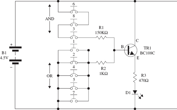
FIGURE 15-2 The circuit diagram for the electronic security keypad
How the Circuit Works
The security keypad circuit is made up of four building blocks: power supply, input, control circuitry (NPN transistor switch), and output. This circuit is powered by three 1.5 volt AA batteries that are wired in series to create a 4.5 volt power supply. The eight normally open push-button switches (SW1–SW8) form the input part of this circuit. The transistor switching circuitry is based around components R1, R2, and TR1. The LED (D1) and its series resistor (R3) create the output part of this circuit.
Before the control circuitry is explained, take a closer look at the way that the eight switches are wired together. You will notice that switches 3, 6, and 8 are wired in series, which means that in order for the positive rail of the battery to reach resistor R1, all of these switches have to be pressed simultaneously. This type of configuration is called an AND logic circuit, because switch 3 AND switch 6 AND switch 8 have to be pressed at the same time to operate the circuit. As you learn more about electronics you will find out that AND circuits are used in computer and digital circuits (you can read more about this in the summary).
INTERESTING FACTThe way that a logic gate operates can be shown in the form of a table, called a truth table. The truth table shows the various ways that the input connections can be switched on or off and how this affects the output. Digital circuits only have two possible circuit states, either on (represented by a binary number 1) or off (represented by a binary number 0), and this is why digital circuits use binary numbers at their heart. Binary numbers are different from decimal numbers because they only contain numbers 0 and 1, rather than numbers 0 to 9.
The truth table for an AND circuit with two switches is shown in Table 15-1. The truth table shows that the only time that the output switches on is when both switch 1 AND switch 2 is switched on; the binary number for each state is also shown in brackets.
TABLE 15-1 AND Logic for a Two-Switch Circuit

There are two types of circuit symbol that you will come across for an AND logic gate and they look like this:

The two lines on the left of each symbol represent the two inputs, and the line on the right of each symbol is the output.
Look at switches 1, 2, 4, 5, and 7 in Figure 15-2 and you’ll notice that these switches are connected up differently from the other three. These switches are wired in parallel, which means that in order for the negative rail of the battery to reach resistor R2, any one of the switches can be pressed. This type of configuration is called an OR logic circuit, because switch 1 OR switch 2 OR switch 4 OR switch 5 OR switch 7 has to be pressed to operate the circuit.
The logic table for an OR circuit with only two push-button switches is shown in Table 15-2.
TABLE 15-2 OR Logic for a Two-Switch Circuit
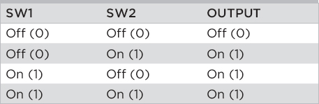
The truth table shows that the output switches on whenever either switch 1 OR switch 2 is switched on; the binary number for each state is also shown in brackets.
There are two types of circuit symbol that you will come across for an OR gate and they look like this:

Again, the two lines on the left of each symbol represent the two inputs and the line on the right of each symbol is the output.
Now that you understand how the switch configurations work, let’s look at the control circuitry.
Here’s how the circuit works: Switches 3, 6, and 8 must to be pressed at the same time to allow the positive battery rail to feed through resistor R1, which drives the base of the NPN transistor and in turn illuminates the LED (D1). This is the secret code to operate the security keypad.
This in itself makes a pretty secure keypad. We’ll set it up to make it even more secure, however, so that if a person presses another switch simultaneously with the other three, a circuit pathway to the negative rail of the circuit is created, and this will stop the positive signal reaching the base of the transistor, so the LED doesn’t illuminate. This circuit configuration creates quite a secure keypad, as you will soon see when you build the experiment.
It’s important that the resistor R1 has a high resistance, because when the secret code is pressed on the keypad, plus any other key, the battery voltage feeds through both resistors, creating a short-circuit. If the resistor has a low resistance, more current is drawn from the battery in this state, and this could cause the resistor to get too hot.
Things You’ll Need
The components that you will need for this experiment are outlined in the following table. Prepare the items that you need before starting the experiment.

 NOTE
NOTEThe Appendix Code column of the table refers to specific parts that I used in this experiment. Information about sourcing these parts is outlined in the Appendix.
The Breadboard Layout
The breadboard layout for the security keypad experiment is shown in Figure 15-3.
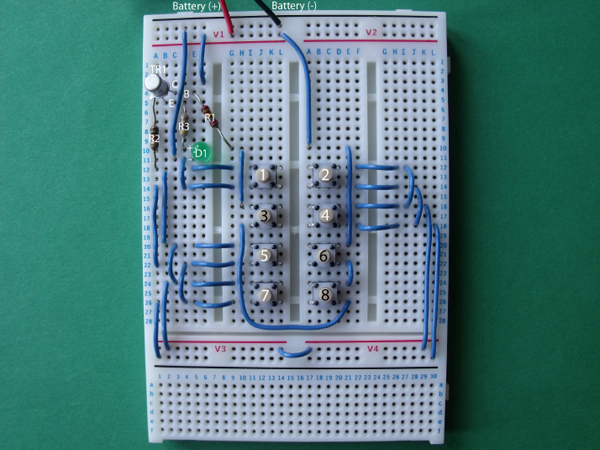
FIGURE 15-3 The breadboard layout for the security keypad experiment
The breadboard might look complicated, because it contains quite a few wire links. Be careful when building this experiment, and double-check to make sure your wiring matches what’s shown in the figure. Refer to the close-up photographs in Figures 15-4 and 15-5, which show more details of the wiring.

FIGURE 15-4 Close-up of the wiring around the transistor; notice the transistor and LED connections
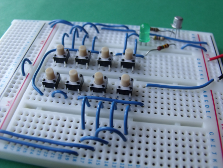
FIGURE 15-5 Close-up of the wiring around the switches
Time to Experiment!
Once you have finished building the breadboard layout, connect the battery to the circuit, and you should find that the LED is not illuminated. Now press push buttons 3, 6, and 8 at the same time, as shown in Figure 15-6. Keep them pressed, and the LED should illuminate. This is the secret code that activates the LED. In a real-life security application, this might activate a relay to unlock a door, for example.
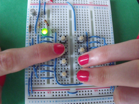
FIGURE 15-6 Pressing the secret buttons to active the LED
This is the only button sequence that will activate the LED. Now try removing one or two of your fingers from any of these three buttons, and the LED no longer illuminates. This happens because these buttons are wired in series to form an AND gate, as explained earlier, and this means that all three buttons have to be pressed at once to complete the circuit.
Press the three buttons again to illuminate the LED, and then press any of the other buttons at the same time. The LED switches off, because these five switches are wired in parallel and create an OR gate, as explained earlier in this chapter.
You have built a secret keypad that isn’t that easy to crack, unless you know which three buttons to press. Even if you start to press random buttons, it will be very difficult to figure out the code and keep the LED illuminated. Try it out on your friends to see if they can crack the code. You don’t need to tell them that they have to press three buttons at once; just ask them to see if they can press the buttons in a certain way to make the LED illuminate for more than 3 seconds. They may discover the secret code eventually, but it will probably take them a while to figure it out.
You might also want to play around with the switch wiring to make the secret code work on a different selection of buttons. The breadboard layout that I put together makes it fairly easy to figure out the wiring of the buttons if you understand electronics, so you might want to use longer interconnecting wires to make the wiring look untidy and to make it more difficult to figure out the secret code.
Summary
In this experiment you learned how two types of logic gates operate and built them into an interesting circuit. Six main logic gates are available to use in electronic circuits: AND, OR, NOT, NAND, NOR, and XOR. The NOT, NAND, NOR, and XOR logic gates are not covered in this book, but you might want to search for them on the Internet and investigate how these logic gates differ from the two described in this chapter. Logic gates are very important in digital circuits; for example, some of the complex ICs inside your home PC will contain logic circuits.
..................Content has been hidden....................
You can't read the all page of ebook, please click here login for view all page.