
The I2C bus is a convenient hardware system mainly because it requires only two wires for communication. The bus is also known by other names, such as the IIC (inter-integrated circuit) or TWI (two-wire interface). Phillips Semiconductor developed the I2C bus, which Intel later extended with the SMBus protocol. These are largely interchangeable, but I will focus on I2C in this chapter.
With the utility of the I2C bus, it is no surprise that the STM32 platform includes a hardware peripheral for it. This chapter will explore how to utilize the peripheral in concert with the PCF8574 GPIO extender device attached to the bus.
The I2C Bus
One of the hallmarks of I2C as a serial communications bus is that it requires only two wires. The power supply and ground connections are not included in this count. The two communication lines involved are the following:
System clock (usually labeled SCL)
System data (usually labeled SDA)
Each of these lines rests at a high voltage level (usually at 5 or 3.3 volts). Any device on the bus can generate a data signal by pulling the line down low (zero volts). This works well for open-collector (bipolar) or open-drain (FET) transistors. When the transistor is active, they act like a switch shorting the bus line to ground. When the bus is idle, a pullup resistor pulls the voltage of the line high. For this reason, both I2C lines operate with at least one pullup resistor.
Master and Slave
With every device on the bus able to pull the lines low, there must be some sort of protocol to keep things organized. Otherwise, the bus would have multiple conversations going on with no receivers making sense of the garbled messages. For this reason, the I2C protocol often uses one master and many slave devices. In more-complex systems, it is possible to have more than one master controller, which is out of scope for this chapter.
The master device always starts the conversation and drives the clock signal. The exception to the SCL line’s being driven by the master is that slaves can sometimes stretch the clock to buy extra time (when it is supported by the master). Clock stretching occurs when the slave device continues to hold the SCL line low after the master has released it.
Slave devices only respond when spoken to. Each slave has a unique 7-bit device address so that it knows when a bus message has been sent to it. This is one area where I2C differs from the SPI bus. Each I2C device is addressed by an address, while SPI devices are selected by a chip-select line.
Start and Stop
The I2C is idle when both the SDA and SCL lines are pulled high. In this case, no device—master or slave—is pulling the bus lines low.
The start of an I2C transaction is indicated by the following events:
The SCL line remains high.
The SDA line is pulled down.
Step two usually happens within a clock cycle, although it need not be precisely so. When the bus is idle, it is enough to see the SDA line going low while the SCL remains high. Figure 11-1 illustrates the start, stop, and repeated start I2C signals.
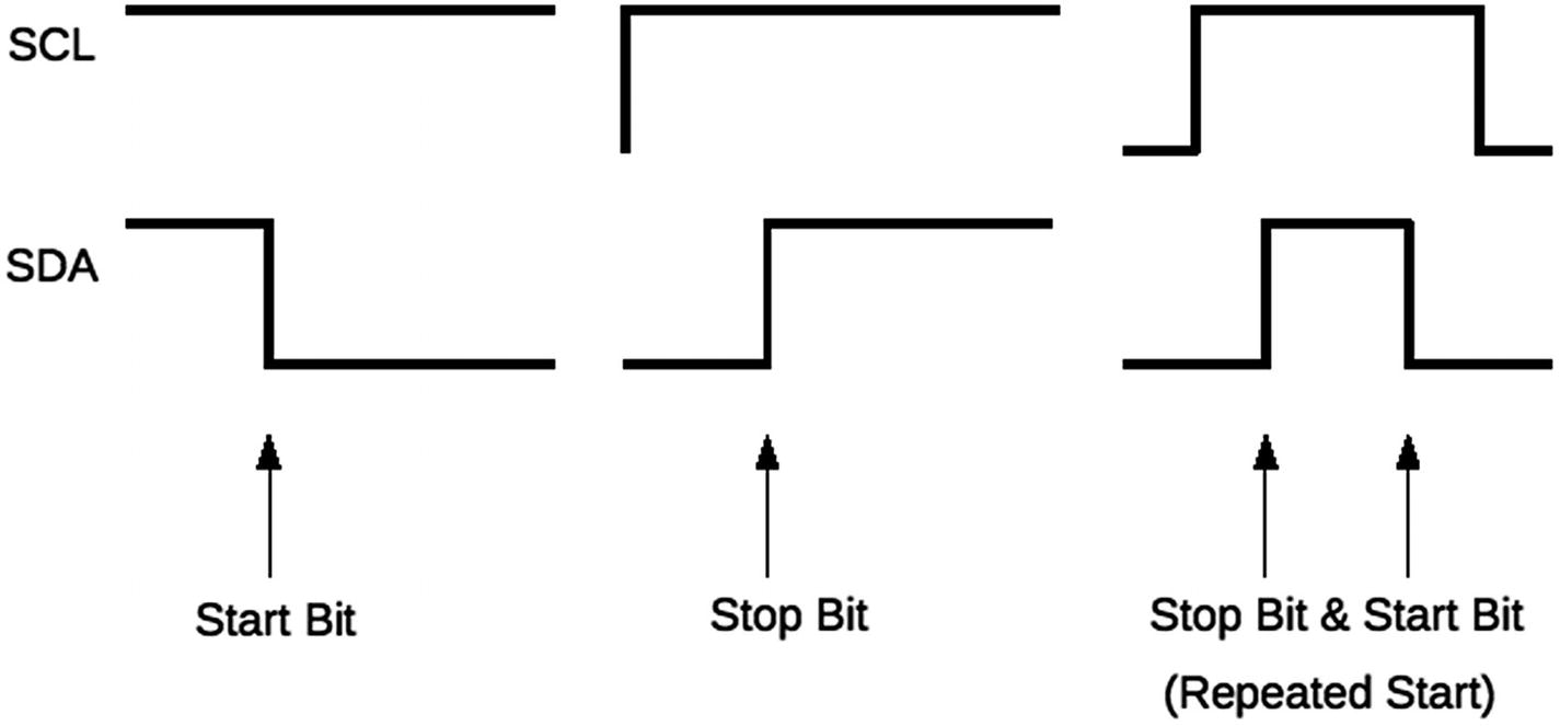
Figure 11-1 I2C start, stop, and repeated start bit signals
The repeated start is both an optimization of the stop and start and a way to hold the bus while continuing with a longer I2C transaction. Later, we’ll discuss this further.
Data Bits
Data bits are transmitted in concert with a high-to-low transition in the clock (SCL) signal. Figure 11-2 illustrates.
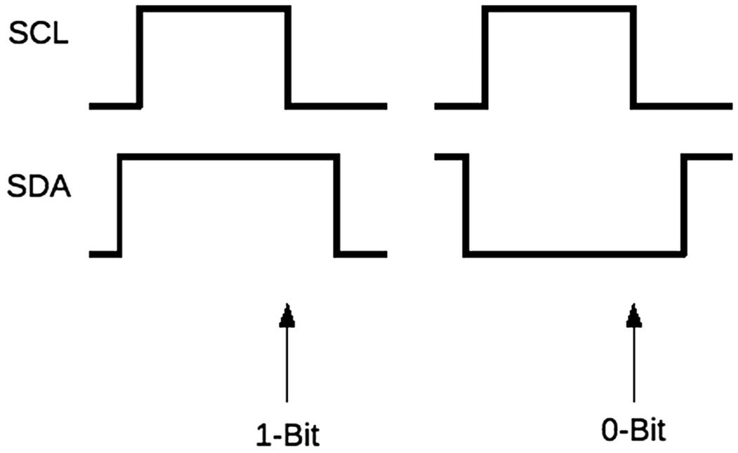
Figure 11-2 I2C data bit signals
The sampling of the SDA bus line occurs where the arrows are shown. The high or low state of the SDA line is read at the point where the SCL line is pulled low (by the master).
I2C Address
Before we look at the whole bus transaction, let’s describe the address byte, which is used to identify the slave device that is expected to respond (Figure 11-3). In addition to the address, a read/write bit indicates the intention to read or write from/to the slave device.

Figure 11-3 I2C 7-bit address format
The 7 bits of address are shifted up 1 bit in the address byte, while the read/write bit is rightmost. The read/write bit is defined as follows:
1-bit indicates that a read operation from the slave device will follow
0-bit indicates that a write operation to the slave device will follow
The address and read/write bit always follow a start or repeated start bit on the I2C bus. The start bit requires the I2C controller to check that the bus is not in use by another master; it does this by using a bus arbitration procedure (when multi-master is supported). But once bus access is won, the bus is owned by the controller until it is released with a stop bit.
The repeated start allows the current transaction to continue without further bus arbitration. Since an address and read/write bit must follow, this allows multiple slaves to be serviced with one transaction. Alternatively, the same slave may be addressed but be accessed with a different read/write mode.
Tip
Sometimes people report that slave addresses shifted up by one bit as they were sent. This has the effect of multiplying the address by two. The address 0x42 when shifted right is actually 0x21. Watch out for this in documentation.
I2C Transactions
Figure 11-4 illustrates a write and a read transaction (where no repeated start is used).
Figure 11-4 I2C write transaction and a read transaction
The upper portion of Figure 11-4 illustrates a simple write transaction. The basic train of events for the illustrated write are as follows:
The I2C controller gains control of the bus and emits a start bit.
The master (controller) writes out seven address bits followed by a 0-bit, indicating that this will be a write transaction.
The slave device acknowledges the request and pulls the data line low during the ACK (acknowlege) bit. If no slave responds, the data line will float high and cause a NAK (negative acknowlege) to be received by the controller instead.
Because this is a write transaction, the data byte is written out.
The slave device acknowledges the receipt of the data byte by pulling down the data line during the ACK bit time.
The master is not sending any more data, so it writes a stop bit and releases the I2C bus.
The read request is similar:
The I2C controller gains control of the bus and emits a start bit.
The master (controller) writes out seven address bits followed by a 1-bit, indicating that this will be a read transaction.
The slave device acknowledges the request and pulls the data line low during the ACK bit. If no slave responds, the data line will float high and cause a NAK to be received by the controller instead.
Because this is a read transaction, the master continues to write out clock bits to allow the slave device to synchronize its data response back to the master.
With each clock pulse, the slave device writes out the eight data bytes to the master controller.
During the ACK time, the master controller normally sends a NAK when no more bytes are to be read.
The controller sends a stop bit, which always ends the transaction with the slave (regardless of the last ACK/NAK sent).
PCF8574 GPIO Extender
To exercise the I2C bus in this chapter, we’ll be using the PCF8574 GPIO extender chip (Figure 11-5). This is a great chip for adding additional GPIO lines, provided that you don’t need high speed (the demo operates the I2C bus at 100 kHz).
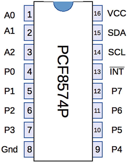
Figure 11-5 Pinout of the PCF8574P
The +3.3 volts power is applied to pin 16, while the grounded connection is pin 8. Pins A0 through A2 are used to select the chip’s slave address (Table 11-1). Pins P0 through P7 are the GPIO databit lines, which can be input or output. Pin 14 connects to the clock line (SCL), while pin 15 connects to the data line (SDA). Pin 13 can be used for notification.
Table 11-1 PCF8574 Address Configuration
A0 | A1 | A2 | PCF8574 Address | PCF8574A Address |
|---|---|---|---|---|
0 | 0 | 0 | 0x20 | 0x38 |
0 | 0 | 1 | 0x21 | 0x39 |
0 | 1 | 0 | 0x22 | 0x3A |
0 | 1 | 1 | 0x23 | 0x3B |
1 | 0 | 0 | 0x24 | 0x3C |
1 | 0 | 1 | 0x25 | 0x3D |
1 | 1 | 0 | 0x26 | 0x3E |
1 | 1 | 1 | 0x27 | 0x3F |
Address lines A0 through A2 are programmed as zeros when grounded and as 1-bits when connected to V cc (+3.3 volts in this demo). If you have the PCF8575A chip, then the address should be taken from the right column. The earlier PCF8574 chip uses hexadecimal addresses in the left column of the table.
I2C Circuit
Figure 11-6 illustrates three PCF8574P devices attached to the STM32 through the I2C bus.

Figure 11-6 STM32 attached to three PCF8574P slave devices using the I2C bus
The schematic looks a little busy, but it’s not that bad. Notice that the I2C bus consists only of a pair of lines, SCL and SDA, originating from the STM32. These two lines are pulled high by resistors R1 and R2, respectively. Each slave device is also connected to these bus lines, allowing each of these to respond when it recognizes its slave address.
Notice how IC1, IC2, and IC3 each have a different wiring for the address pins A0, A1, and A2. This configures each device to respond to a different slave address (review Table 11-1). These addresses must be unique.
The PCF8574  Line
Line
The remaining connections in Figure 11-6 are power and the ![]() line. The
line. The ![]() line is an optional bus component that has nothing to do with the I2C bus itself. You might not even attach all PCF8574P devices to the
line is an optional bus component that has nothing to do with the I2C bus itself. You might not even attach all PCF8574P devices to the ![]() line if they never get used for GPIO input.
line if they never get used for GPIO input.
The ![]() line signals that an input GPIO has changed and is usually attached to a microprocessor interrupt line. This saves the MCU from continuously polling the I2C devices to see if a button was pressed, for example. If any input line changes from high to low, or low to high, the open-drain transistor in the PCF8574 is activated and pulls the
line signals that an input GPIO has changed and is usually attached to a microprocessor interrupt line. This saves the MCU from continuously polling the I2C devices to see if a button was pressed, for example. If any input line changes from high to low, or low to high, the open-drain transistor in the PCF8574 is activated and pulls the ![]() line low. This remains low until the device has its interrupt “serviced.” A simple read or write to the peripheral is all that is necessary to service the interrupt.
line low. This remains low until the device has its interrupt “serviced.” A simple read or write to the peripheral is all that is necessary to service the interrupt.
The ![]() line does not identify which slave device has registered a change. The MCU must still poll its participating slave devices to see where the change occurred.
line does not identify which slave device has registered a change. The MCU must still poll its participating slave devices to see where the change occurred.
There is a small limitation that is important to keep in mind. If the GPIO level change occurs too quickly, no interrupt will be generated. It is also possible for a GPIO change event to occur during the ACK/NAK cycle when the interrupt is being cleared. An interrupt occurring then can also be lost. The NXP (NXP Semiconductors) datasheet indicates that it takes 4 μs from the sensing of a GPIO change to the activation of the ![]() line. The remaining time will consist of the MCU’s interrupt response and software-handler processing.
line. The remaining time will consist of the MCU’s interrupt response and software-handler processing.
PCF8574 Configuration
The NXP Semiconductors datasheet describes the I/O ports as quasi-bidirectional. What this means is that the GPIO ports (P0 through P7) can be used as outputs or be read as inputs directly, without any configuration through a device register.
To send an output value, you simply write to the PCF8574 device over the I2C bus. Input GPIOs, on the other hand, require a little trick—where you want GPIO inputs, you write a 1-bit to the GPIO port first. To see how this works, review Figure 11-7.
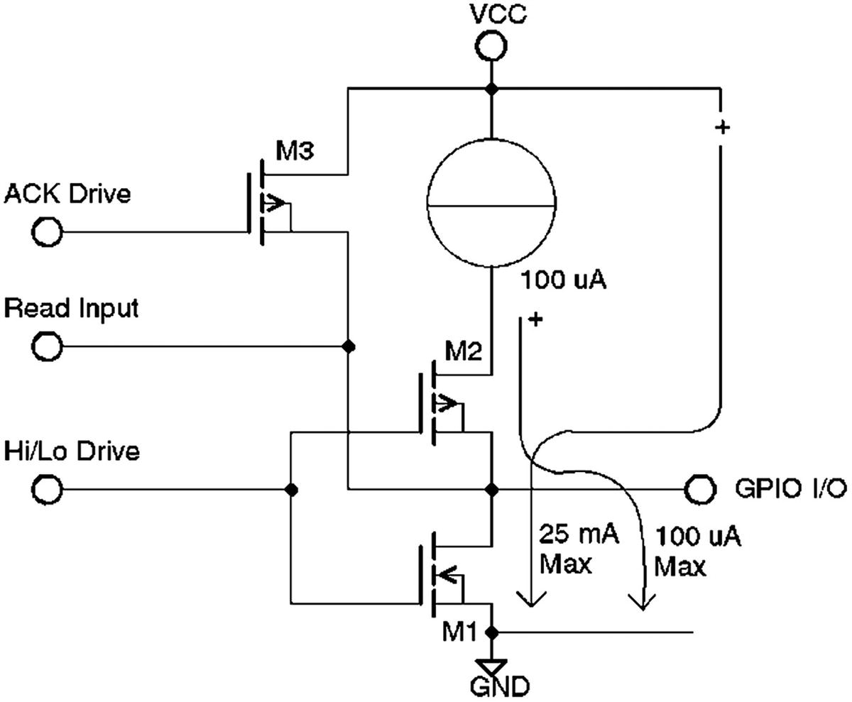
Figure 11-7 PCF8574 simplified GPIO circuit
Start at the top of the diagram where V cc (+3.3 volts) is located. Within the chip is a 100 μA constant-current regulator in series with transistors M2 and M1. Consequently, when a high (1-bit) is written to the GPIO port, transistor M2 is turned on and M1 is turned off (driven by the “hi/lo drive” internal to the chip). Transistor M3 is off at this time.
If you short circuited the GPIO pin to ground, the constant-current regulator limits the current to 100 μA as it flows through M2 and out the GPIO pin to ground (rightmost arrow in Figure 11-7). While shorted like this, the internals of the PCF8574 are able to sense a low on the internal “Read Input” connected to the GPIO, which is read back as a 0-bit. By writing a 1-bit to the GPIO, you allow an external circuit to bring the voltage level low, or leave it pulled high. The current is always limited to a trickle of 100 μA, so no harm is done.
If, instead, the GPIO pin were written as a 0-bit, transistor M1 would always be turned on, shorting out the GPIO level. The “Read Input” would always be sensed as a 0-bit as a result. By the simple rule of writing a 1-bit to the GPIO, you can sense when it is pulled to ground as an input.
PCF8574 GPIO Drive
The quasi-bidirectional design of the GPIO has a consequence. You’ve already seen that the shorted GPIO output is current-limited to 100 μA. This means that the GPIO cannot act as a current source for an LED. A typical LED needs about 10 mA of current, which is 100 times what this GPIO is capable of supplying!
However, transistor M1 is able to handle a maximum of 25 mA if you use the GPIO pin to sink power for the LED. Figure 11-8 illustrates how to drive an LED.
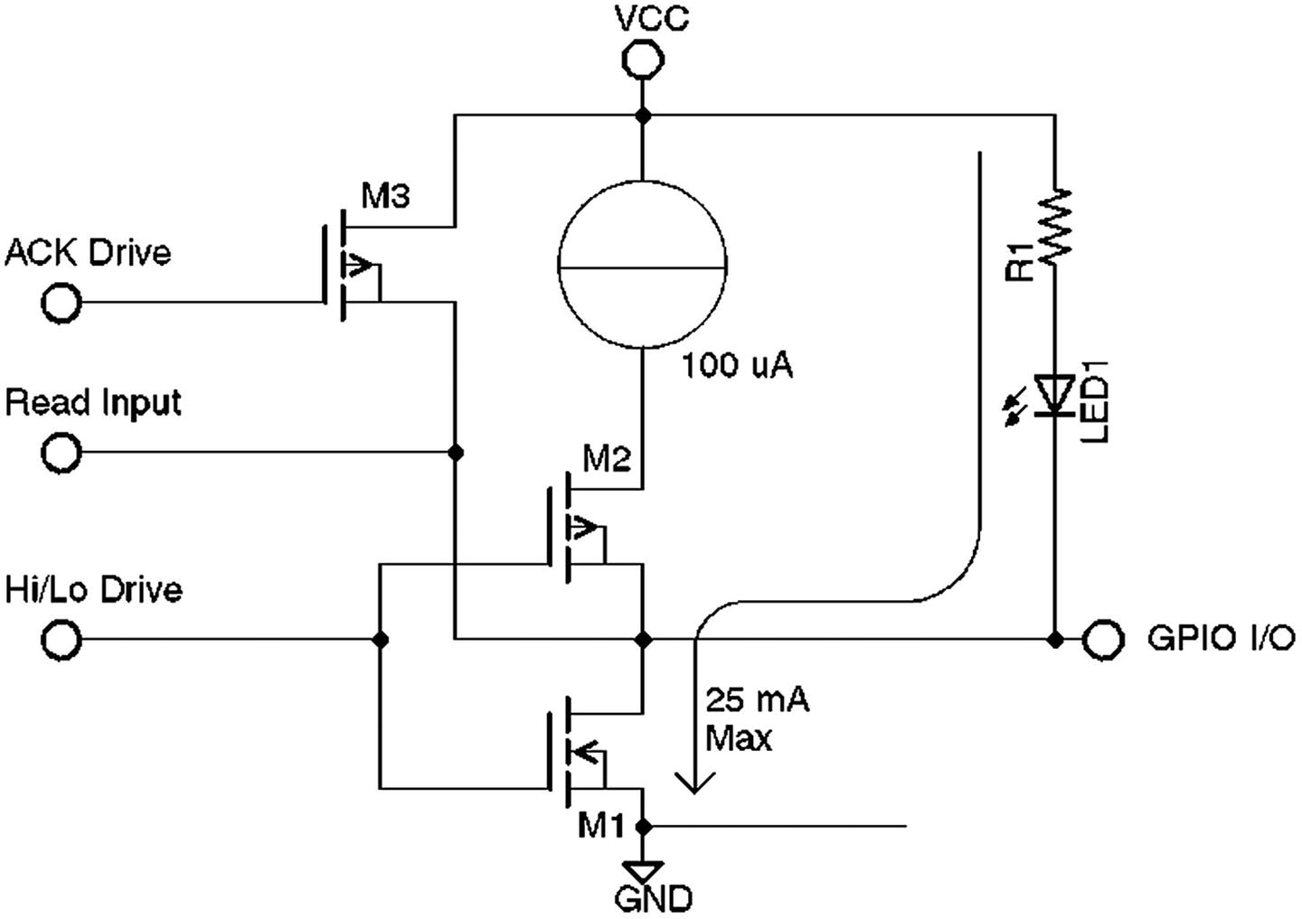
Figure 11-8 Driving higher-current loads with the PCF8574
The LED and resistor R1 are supplied from V cc , which is not current limited. So, M1 acts as a switch to sink the current to ground, lighting the LED. The logic impact of this is that you need to write a 0-bit to turn the LED on.
Note
While the high drive of the PCF8574 is limited to 100 μA, this is sufficient for driving other CMOS (complementary metal oxide semiconductor) signal inputs.
Wave Shaping
When the GPIO output is written as a 1-bit, only 100 μA of current is available to pull it up to V cc . This presents a bit of a problem when it is currently at low potential, resulting in a slow rise time.
The designers of the PCF8574 included a circuit with transistor M3 (Figure 11-8), which is normally off. However, when the device is written to, each GPIO that is receiving a 1-bit gets a boost from M3 during the I2C ACK/NAK cycle. This helps to provide a snappy low-to-high transition on the outputs. Once the ACK/NAK cycle is completed, M3 turns off again, leaving the 100 μA current limiter to maintain the high output.
Demo Circuit
Figure 11-9 illustrates the final circuit for the demo program. The noteworthy changes are that only one PCF8574 chip is used, using two LEDs and one push button.
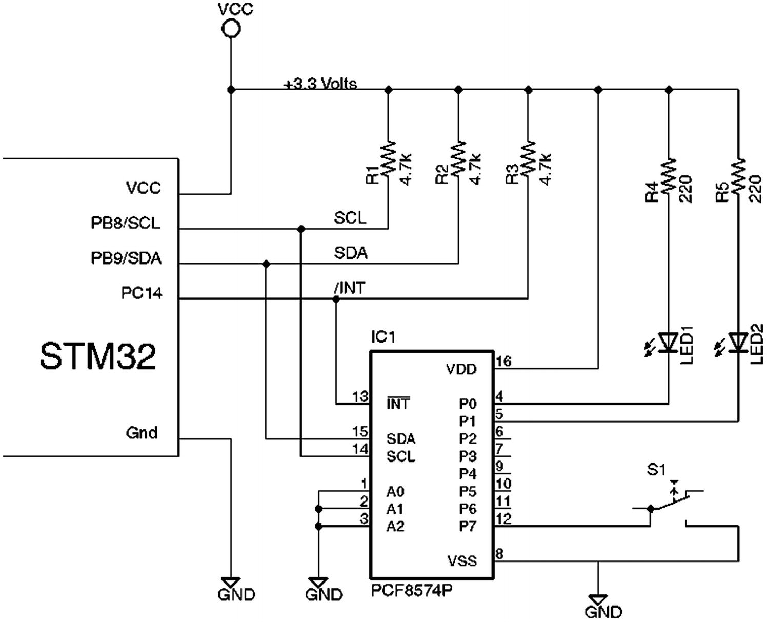
Figure 11-9 The demo I2C schematic with LEDs and push button
When wiring this circuit up, don’t forget to include the pullup resistor R3 so that the idle potential of GPIO PC14 is high. Note also that both LEDs are supplied from the V cc rail so that ports P0 and P1 sink the current to light the LEDs. Port P7 will read the push button, which will be normally high (recall that the port is pulled high by the 100 μA constant-current source within the PCF8574). When the button is pressed, P7 will be pulled to ground, causing a 0-bit to be read.
EXTI Interrupt
The RTC2 project made use of the EXTI interrupt to achieve a separate alarm interrupt. A few more steps are required to achieve an interrupt on PC14 for the /INT interrupt. Let’s look at the software involved. The project software for this chapter is found in this directory:
$ cd ~/stm32f103c8t6/rtos/i2c-pcf8574Initially, we’ll examine the I2C and EXTI setup in the main() routine of main.c (Listing 11-1).
Listing 11-1 The Initial Setup of the I2C Peripheral and EXTI Interrupts
0197: int
0198: main(void) {
0199:
0200:   rcc_clock_setup_in_hse_8mhz_out_72mhz();// For "blue pill"
0201:   rcc_periph_clock_enable(RCC_GPIOB);  // I2C
0202:   rcc_periph_clock_enable(RCC_GPIOC);  // LED
0203:   rcc_periph_clock_enable(RCC_AFIO);   // EXTI
0204:   rcc_periph_clock_enable(RCC_I2C1);   // I2C
0205:
0206:   gpio_set_mode(GPIOB,
0207:       GPIO_MODE_OUTPUT_50_MHZ,
0208:       GPIO_CNF_OUTPUT_ALTFN_OPENDRAIN,
0209:       GPIO6|GPIO7);                    // I2C
0210:   gpio_set(GPIOB,GPIO6|GPIO7);         // Idle high
0211:
0212:   gpio_set_mode(GPIOC,
0213:       GPIO_MODE_OUTPUT_2_MHZ,
0214:       GPIO_CNF_OUTPUT_PUSHPULL,
0215:       GPIO13);                         // LED on PC13
0216:   gpio_set(GPIOC,GPIO13);              // PC13 LED dark
0217:
0218:   // AFIO_MAPR_I2C1_REMAP=0, PB6+PB7
0219:   gpio_primary_remap(0,0);
0220:
0221:   gpio_set_mode(GPIOC,                 // PCF8574 /INT
0222:       GPIO_MODE_INPUT,                 // Input
0223:       GPIO_CNF_INPUT_FLOAT,
0224:       GPIO14);                         // on PC14
0225:
0226:   exti_select_source(EXTI14,GPIOC);
0227:   exti_set_trigger(EXTI14,EXTI_TRIGGER_FALLING);
0228:   exti_enable_request(EXTI14);
0229:   nvic_enable_irq(NVIC_EXTI15_10_IRQ);    // PC14 <- /INT
Lines 201 through 204 enable clocks that are needed by GPIOB (for I2C), GPIOC (for LED- and PC14-sensing ![]() ), EXTI, and the I2C peripheral itself. Line 206 configures GPIO PB6 and PB7 for open-drain operation for the I2C peripheral. Line 210 may not be strictly necessary, but until the I2C peripheral is configured, the I2C bus lines should be allowed to be pulled high.
), EXTI, and the I2C peripheral itself. Line 206 configures GPIO PB6 and PB7 for open-drain operation for the I2C peripheral. Line 210 may not be strictly necessary, but until the I2C peripheral is configured, the I2C bus lines should be allowed to be pulled high.
Line 219 configures I2C1 to use PB6 and PB7. The gpio_primary_remap() libopencm3 function can be used to make other choices. PB6 and PB7 are extra useful because these have 5-volt-tolerant inputs.
Line 221 sets up GPIO PC14 to be an input in floating mode. This line will be pulled high by R3 in Figure 11-9.
Lines 226 through 229 configure the EXTI interrupt. The exti_select_source() function chooses GPIO PC14 to be added to the list of potential interrupt sources. Line 227 then configures that the interrupt should occur when the signal falls from high to low. Finally, line 228 enables the EXTI peripheral to request interrupts. The call to nvic_enable_irq() enables the interrupt vector NVIC_EXTI15_10_IRQ. When this interrupt occurs, the entry point exti15_10_isr() will be called.
To save you much head scratching if you’re working from the ST Microelectronics datasheet (RM0008), Table 11-2 is provided. The datasheet isn’t clear, in my opinion, about how the interrupts are supported for EXTI. The table shows that lines zero through four have their own private interrupt vector. But for GPIO ports numbering 5 to 9, or 10 to 15, the interrupt vectors are more widely shared.
Table 11-2 The List of EXTI STM32F103 Interrupts and ISR Routine Names
Interrupt | ISR Routine | Description |
|---|---|---|
NVIC_EXTI0_IRQ | exti0_isr() | Line 0: PA0/PB0/PC0 |
NVIC_EXTI1_IRQ | exti1_isr() | Line 1: PA1/PB1/PC1 |
NVIC_EXTI2_IRQ | exti2_isr() | Line 2: PA2/PB2/PC2 |
NVIC_EXTI3_IRQ | exti3_isr() | Line 3: PA3/PB3/PC3 |
NVIC_EXTI4_IRQ | exti4_isr() | Line 4: PA4/PB4/PC4 |
NVIC_EXTI9_5_IRQ | exti9_5_isr() | Lines 5 to 9: PA5-9/PB5-9/PC5-9 |
NVIC_EXTI15_10_IRQ | exti15_10_isr() | Lines 10 to 15: PA10-15/PB10-15/PC10-15 |
NVIC_PVD_IRQ | pvd_isr() | Line 16: Power |
NVIC_RTC_ALARM_IRQ | rtc_alarm_isr() | Line 17: RTC Alarm |
NVIC_USB_WAKEUP_IRQ | usb_wakeup_isr() | Line 18: USB Wakeup |
I2C Software
The source code to drive the I2C peripheral has been placed in the source module i2c.c. The first function of interest is i2c_configure() , illustrated in Listing 11-2.
Listing 11-2 I2C Configuration
0061: void
0062: i2c_configure(I2C_Control *dev,uint32_t i2c,uint32_t ticks) {
0063:
0064:   dev->device = i2c;
0065:   dev->timeout = ticks;
0066:
0067:   i2c_peripheral_disable(dev->device);
0068:   i2c_reset(dev->device);
0069:   I2C_CR1(dev->device) &= ~I2C_CR1_STOP;    // Clear stop
0070:   i2c_set_standard_mode(dev->device);       // 100 kHz mode
0071:   i2c_set_clock_frequency(dev->device,I2C_CR2_FREQ_36MHZ); // APB Freq
0072:   i2c_set_trise(dev->device,36);            // 1000 ns
0073:   i2c_set_dutycycle(dev->device,I2C_CCR_DUTY_DIV2);
0074:   i2c_set_ccr(dev->device,180);             // 100 kHz <= 180 * 1 /36M
0075:   i2c_set_own_7bit_slave_address(dev->device,0x23);
0076:   i2c_peripheral_enable(dev->device);
0077: }
A structure named I2C_Control is passed in as the first argument to hold the configuration. The I2C peripheral address is passed in the argument i2c, which will be I2C1 for this demo. The last argument defines a timeout to be used, specified in ticks. These values are preserved in I2C_Control in lines 64 and 65 for later use.
Lines 67 to 69 clear and reset the I2C peripheral so that if it is stuck, it can be “unstuck.” One of the disadvantages of I2C is that the protocol can sometimes hang if unpleasant things happen on the bus.
Lines 70 to 76 configure the I2C peripheral and enable it. Line 75 is only necessary if you want to operate the controller in slave mode.
Testing I2C Ready
Before any I2C operations can be initiated, you must test whether the device is busy. Otherwise, your request will likely be ignored or will impair the current operation. Listing 11-3 shows the routine used.
Listing 11-3 Testing for I2C Ready
0083: void
0084: i2c_wait_busy(I2C_Control *dev) {
0085:
0086:   while ( I2C_SR2(dev->device) & I2C_SR2_BUSY )
0087:       taskYIELD();               // I2C Busy
0088:
0089: }
This routine uses libopencm3 routines and macros to manage the peripheral. If the device is busy, however, the control is passed to other FreeRTOS tasks using the taskYIELD() statement.
Start I2C
To initiate an I2C bus transaction, the peripheral must perform a “start” operation. This can involve bus arbitration if there are multiple masters being used. Listing 11-4 shows the routine used by the demo.
Listing 11-4 I2C Start Function
0095: void
0096: i2c_start_addr(I2C_Control *dev,uint8_t addr,enum I2C_RW rw) {
0097:   TickType_t t0 = systicks();
0098:
0099:   i2c_wait_busy(dev);                  // Block until not busy
0100:   I2C_SR1(dev->device) &= ~I2C_SR1_AF; // Clear Acknowledge failure
0101:   i2c_clear_stop(dev->device);       // Do not generate a Stop
0102:   if ( rw == Read )
0103:       i2c_enable_ack(dev->device);
0104:   i2c_send_start(dev->device);         // Generate a Start/Restart
0105:
0106:   // Loop until ready:
0107:   while ( !((I2C_SR1(dev->device) & I2C_SR1_SB)
0108:     && (I2C_SR2(dev->device) & (I2C_SR2_MSL|I2C_SR2_BUSY))) ) {
0109:       if ( diff_ticks(t0,systicks()) > dev->timeout )
0110:           longjmp(i2c_exception,I2C_Addr_Timeout);
0111:       taskYIELD();
0112:   }
0113:
0114:   // Send Address & R/W flag:
0115:   i2c_send_7bit_address(dev->device,addr,
0116:       rw == Read ? I2C_READ : I2C_WRITE);
0117:
0118:   // Wait until completion, NAK, or timeout
0119:   t0 = systicks();
0120:   while ( !(I2C_SR1(dev->device) & I2C_SR1_ADDR) ) {
0121:       if ( I2C_SR1(dev->device) & I2C_SR1_AF ) {
0122:           i2c_send_stop(dev->device);
0123:           (void)I2C_SR1(dev->device);
0124:           (void)I2C_SR2(dev->device);     // Clear flags
0125:           // NAK Received (no ADDR flag will be set here)
0126:           longjmp(i2c_exception,I2C_Addr_NAK);
0127:       }
0128:       if ( diff_ticks(t0,systicks()) > dev->timeout )
0129:           longjmp(i2c_exception,I2C_Addr_Timeout);
0130:       taskYIELD();
0131:   }
0132:
0133:   (void)I2C_SR2(dev->device);          // Clear flags
0134: }
The first step is to determine the current tick time in line 97. This allows us to time the operation and time out if necessary. Line 99 waits for the peripheral to become ready. Once ready, line 100 clears an acknowledge failure, if there was one. Line 101 indicates that no stop should be generated.
If the operation is going to be a read, the i2c_enable_ack() is called to allow receipt of the ACK from the slave. The peripheral is then told to generate a start bit in line 104.
Lines 107 and 108 test if the start bit has been generated. If it is not yet generated, lines 109 and 110 test and perform a longjmp() if the operation has timed out. We’ll speak more about the longjmp() acting as an exception later. If not timed out, the FreeRTOS statement taskYIELD() is performed to share the CPU while we wait.
Once the start bit has been generated, execution continues at line 115 to send the slave address and the read/write indicator.
In line 119 we note the time again for another potential timeout. Line 120 waits for the I2C address to be sent, while line 121 tests if the slave device ACKed the request. If no device responds to the address requested, a NAK will be received by default (thanks to the pull-up resistor). If the operation times out, a longjmp() is performed at line 129.
If the operation succeeds, a flag is cleared by calling I2C_SR2() to read the status register.
I2C Write
Once the start bit has been generated and the address sent, if we indicated that a write follows, we must do that next. Listing 11-5 shows the write function used.
Listing 11-5 I2C Write Function
0140: void
0141: i2c_write(I2C_Control *dev,uint8_t byte) {
0142:   TickType_t t0 = systicks();
0143:
0144:   i2c_send_data(dev->device,byte);
0145:   while ( !(I2C_SR1(dev->device) & (I2C_SR1_BTF)) ) {
0146:       if ( diff_ticks(t0,systicks()) > dev->timeout )
0147:           longjmp(i2c_exception,I2C_Write_Timeout);
0148:       taskYIELD();
0149:   }
0150: }
Line 142 notes the time for a possible timeout. Line 144 ships the data byte to the I2C peripheral to be sent serially on the bus. Line 145 tests for the completion of this operation and times out with a longjmp() if necessary (line 147). Aside from sharing the CPU with taskYIELD(), the function returns when successful.
I2C Read
If the intention was to read, the read routine is used to read a data byte. Listing 11-6 illustrates the code used.
Listing 11-6 The I2C Read Function
0157: uint8_t
0158: i2c_read(I2C_Control *dev,bool lastf) {
0159:   TickType_t t0 = systicks();
0160:
0161:   if ( lastf )
0162:       i2c_disable_ack(dev->device);    // Reading last/only byte
0163:
0164:   while ( !(I2C_SR1(dev->device) & I2C_SR1_RxNE) ) {
0165:       if ( diff_ticks(t0,systicks()) > dev->timeout )
0166:           longjmp(i2c_exception,I2C_Read_Timeout);
0167:       taskYIELD();
0168:   }
0169:
0170:   return i2c_get_data(dev->device);
0171: }
One of the unusual aspects of the i2c_read() function presented is that it has a Boolean lastf flag. This is set true by the caller if it is the last or only byte to be read. This gives the slave device a head’s up that it can relax (some slaves must prefetch data in order to stay in step with the master controller). This is the purpose of the call on line 162.
Otherwise, it is a matter of status testing in line 164 and timing out in line 166 if the operation takes too long. Otherwise, the CPU is shared with taskYIELD(), and the byte is returned in line 170.
I2C Restart
The i2c_write_restart() routine partially shown in Listing 11-7 provides the ability to change from a write request into another request (read or write) without stopping. You can continue with the same slave device (by repeating the same slave address) or switch to another. This is significant when there are multiple I2C masters because this permits another message without renegotiating the access to the bus.
Listing 11-7 The “Secret Sauce” to Performing an I2C Restart Transaction
void
0179: i2c_write_restart(I2C_Control *dev,uint8_t byte,uint8_t addr) {
0180:   TickType_t t0 = systicks();
0181:
0182:   taskENTER_CRITICAL();
0183:   i2c_send_data(dev->device,byte);
0184:   // Must set start before byte has written out
0185:   i2c_send_start(dev->device);
0186:   taskEXIT_CRITICAL();
Some of this kind of information is difficult to tease from the STM32 reference manual (RM0008). However, careful attention to the fine print and footnotes can sometimes yield gold nuggets. The manual says:
In master mode, setting the START bit causes the interface to generate a ReStart condition at the end of the current byte transfer.
By making lines 182 to 186 a critical section, you guarantee that you request another “start” prior to the current I2C’s write being completed.
Demo Program
Listing 11-8 illustrates the main loop of the demo program. Most of it is straightforward, but there are a few things that are noteworthy. After the I2C device is configured in line 131, the inner loop begins at line 134. As long as there is no keyboard input, this loop continues writing and reading from the PCF8574 chip.
Listing 11-8 Main Loop of the Demo Program
0116: static void
0117: task1(void *args __attribute__((unused))) {
0118:   uint8_t addr = PCF8574_ADDR(0);    // I2C Address
0119:   volatile unsigned line = 0u;       // Print line #
0120:   volatile uint16_t value = 0u;      // PCF8574P value
0121:   uint8_t byte = 0xFF;               // Read I2C byte
0122:   volatile bool read_flag;           // True if Interrupted
0123:   I2C_Fails fc;                      // I2C fail code
0124:
0125:   for (;;) {
0126:       wait_start();
0127:       usb_puts("
I2C Demo Begins "
0128:           "(Press any key to stop)

");
0129:
0130:       // Configure I2C1
0131:       i2c_configure(&i2c,I2C1,1000);
0132:
0133:       // Until a key is pressed:
0134:       while ( usb_peek() <= 0 ) {
0135:           if ( (fc = setjmp(i2c_exception)) != I2C_Ok ) {
0136:               // I2C Exception occurred:
0137:               usb_printf("I2C Fail code %d

",
                                    fc,i2c_error(fc));
0138:               break;
0139:           }
0140:
0141:           read_flag = wait_event(); // Interrupt or timeout
0142:
0143:           // Left four bits for input, are set to 1-bits
0144:           // Right four bits for output:
0145:
0146:           value = (value & 0x0F) | 0xF0;
0147:           usb_printf("Writing $%02X "
                            "I2C @ $%02X
",value,addr);
0148: #if 0
0149:           /*********************************************
0150:            * This example performs a write transaction,
0151:            * followed by a separate read transaction:
0152:            *********************************************/
0153:           i2c_start_addr(&i2c,addr,Write);
0154:           i2c_write(&i2c,value&0x0FF);
0155:           i2c_stop(&i2c);
0156:
0157:           i2c_start_addr(&i2c,addr,Read);
0158:           byte = i2c_read(&i2c,true);
0159:           i2c_stop(&i2c);
0160: #else
0161:           /*********************************************
0162:            * This example performs a write followed
0163:            * immediately by a read in one I2C transaction,
0164:            * using a "Repeated Start"
0165:            *********************************************/
0166:           i2c_start_addr(&i2c,addr,Write);
0167:           i2c_write_restart(&i2c,value&0x0FF,addr);
0168:           byte = i2c_read(&i2c,true);
0169:           i2c_stop(&i2c);
0170: #endif
0171:           if ( read_flag ) {
0172:               // Received an ISR interrupt:
0173:               if ( byte & 0b10000000 )
0174:                   usb_printf("%04u: BUTTON RELEASED: "
0175:                       "$%02X; wrote $%02X, "
                            "ISR %d
",
0176:                       ++line,byte,
                            value,isr_count);
0177:               else  usb_printf("%04u: BUTTON PRESSED:  "
0178:                       "$%02X; wrote $%02X, "
                            "ISR %d
",
0179:                       ++line,byte,
                            value,isr_count);
0180:           } else  {
0181:               // No interrupt(s):
0182:               usb_printf("%04u:           "
                        "Read:  $%02X, "
0183:                   "wrote $%02X, ISR %d
",
0184:                   ++line,byte,value,isr_count);
0185:           }
0186:           value = (value + 1) & 0x0F;
0187:       }
0188:
0189:       usb_printf("
Press any key to restart.
");
0190:   }
0191: }
Of particular note is the setjmp() at line 135. Since C lacks the exception mechanism that C++ possesses, the longjmp() was used instead. Our doing a setjmp() at the top of the loop allows us to make several later I2C calls, each with its own points of failure, including timeouts. If any failure occurs, the longjmp() will take the control back to line 135 and return a non-zero failure code. From there the problem can be reported and exited out of the inner loop.
The setjmp/longjmp mechanism does exact a small price, however. Notice that variables line, value, and read_flag are marked volatile (lines 119 to 122). This was necessary to silence the compiler because it warns about those values’ being changed as a result of the longjmp(), should it occur. The setjmp saves a bunch of registers, while the longjmp restores them to bring control back. Any variables still cached in a register would be clobbered by a longjmp.
There are #if, #else, and #endif statements in lines 148, 160, and 170, respectively. By changing line 148 from the value zero to a non-zero value, all transactions will be individual; i.e., the byte will be written out to the PCF8574P in one transaction, followed by a completely separate I2C transaction to read from it.
Leaving line 148 at the value zero allows you to test the I2C restart operation. Lines 166 through 169 perform a write followed by a read in the same transaction.
Demo Session
Perform a build from scratch as follows:
$ make clobber
$ make
arm-none-eabi-gcc ... -o main.elf
arm-none-eabi-size main.elf
   text   data    bss    dec    hex    filename
  13024     28  18200  31252   7a14    main.elf
Ready the device for flashing and perform the following:
$ make flash
arm-none-eabi-objcopy -Obinary main.elf main.bin
/usr/local/bin/st-flash  write main.bin 0x8000000
...
2017-12-09T21:32:12 INFO src/common.c: Flash written and verified!
                                       jolly good!
Now, plug the USB cable in and start minicom, as follows:
$ minicom usbWelcome to minicom 2.7OPTIONS:Compiled on Sep 17 2016, 05:53:15.Port /dev/cu.usbmodemWGDEM1, 21:33:40Press Meta-Z for help on special keysTask1 begun.Press any key to begin.
Once again, the “usb” argument to minicom is the name of the file that you saved your minicom settings to. I used the file named usb in this example.
Once you see “Task1 begun,” press any key. I pressed Return. Once you do that, the I2C device should get configured, and you should start seeing messages of the following form:
I2C Demo Begins (Press any key to stop)Writing $F0 I2C @ $200001: Read: $F0, wrote $F0, ISR 0Writing $F1 I2C @ $200002: Read: $F1, wrote $F1, ISR 0
If you press a key again, the control will stop and then fall out to the outer loop. Pressing a key again will restart the demo in the inner loop.
The values written out to the PCF8574P will increment in the lower four bits. If you attached LEDs to P0 and P1 as in the schematic, you should see them count down in binary. When you press the button, you should see some messages indicating button press and release events.
Writing $F5 I2C @ $20
0006:           Read:  $F5, wrote $F5, ISR 0
Writing $F6 I2C @ $20
0007:           Read:  $F6, wrote $F6, ISR 0
Writing $F7 I2C @ $20
0008: BUTTON PRESSED:  $77; wrote $F7, ISR 4
Writing $F8 I2C @ $20
0009: BUTTON PRESSED:  $78; wrote $F8, ISR 4
Writing $F9 I2C @ $20
0010: BUTTON PRESSED:  $79; wrote $F9, ISR 5
Writing $FA I2C @ $20
0011: BUTTON PRESSED:  $7A; wrote $FA, ISR 6
Writing $FB I2C @ $20
0012: BUTTON PRESSED:  $7B; wrote $FB, ISR 7
Writing $FC I2C @ $20
0013: BUTTON PRESSED:  $7C; wrote $FC, ISR 8
Writing $FD I2C @ $20
0014:           Read:  $7D, wrote $FD, ISR 8
Writing $FE I2C @ $20
0015: BUTTON RELEASED: $FE; wrote $FE, ISR 11
The value shown after ISR shows you how many times the ISR routine was called when the PCF8574P indicated an interrupt. My button was pretty scratchy, and without any debouncing you see several button-press events. Notice that while the button was held down, the upper bit changed from a 1-bit to a 0-bit (for example, $FX changed to a $7X).
Summary
This chapter leaves you well prepared for I2C work. The PCF8574 is a very economical solution for adding more GPIO ports provided you don’t have high speed requirements. At the same time, it provides you with experience in the world of I2C. The PCF8574 has demonstrated that it can generate interrupts so that you don’t have to continually poll for input-line changes. This eases the burden of I2C traffic on the bus.