
The unit that you purchased has likely already been preprogrammed to blink when it is powered up (perhaps you’ve checked this already). This makes it easy to test that it is a working unit. There are a few other important details regarding power, reset, and LEDs that need to be discussed in this chapter. Finally, the use of the ST-Link V2 programmer and a device probe will be covered.
Power
The STM32F103C8T6 PCB, otherwise known as the “Blue Pill” board, has a number of connections, including a few for power. It is not necessary to use all of the power connections at once. In fact, it is best to use only one set of connections. To clarify this point, let’s begin with an examination of your power options. Figure 3-1 illustrates the connections around the edges of the PCB, including power.

Figure 3-1 Power and GPIO connections to the STM32F103C8T6 “Blue Pill” PCB. Power can be supplied to a +5V, +3.3V, or USB port, with the matching voltage. Pins marked as “5V” (with no plus sign) are 5-volt tolerant inputs. Pins marked with a plus sign are for power input.
The four pins at the top end of the board (darker blue) are used for programming the device. Notice that the programming connection labeled DIO is also capable of being a GPIO PA13. Likewise, DCLK is capable of being a GPIO PA14. You’ll discover how configurable the STM32 can be as we go through this book.
At the programming connector, note that the input supply voltage is +3.3 volts. This connection is electrically the same as any of the others that are labeled “+3.3V” around the PCB. These are shown in a light orange.
+3.3V Regulator
The STM32F103C8T6 chip is designed to operate from any voltage from 2 to 3.3 volts. The Blue Pill PCB provides a tiny +3.3-volt regulator labeled “U1” on the underside (see Figure 3-2). My unit used a regulator with an SMD code of 4A2D, which is an XC6204 series part. Yours may vary.
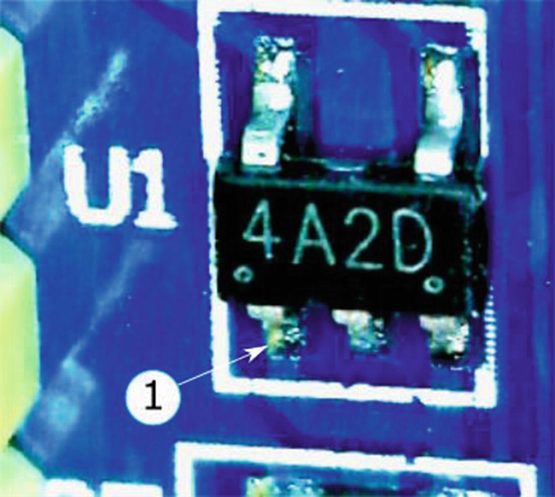
Figure 3-2 The +3.3-volt regulator on the underside of the PCB. Pin 1 of the 4A2D (XC6204 series) regulator chip is marked.
The official schematic for this board specifies the regulator as being the RT9193-33, which supports 300 mA. 1 It is possible that my PCB is a clone using a cheaper regulator chip. My XC6204 series regulator chip is limited to 150 mA. Unless you know the specifics of your unit, it is safest to assume 150 mA is the current limit.
The power performance of the MCU will be examined in a later chapter. But as a starting reference point, the blink program in the device as supplied uses about 30 mA (measured with the +5-volt input supply at 4.97 volts). This measurement includes the small additional current used by the regulator itself.
The datasheet for the STM32F103C8T6 documents the maximum current draw at about 50 mA. This document measurement was obtained with the external clock and all peripherals enabled, while operating in “run mode” at 72 MHz. Subtracting 50 from your regulator max of 150 leaves you a current budget of about 100 mA from the +3.3-volt regulator. It’s always good to know what the limits are!
USB Power/+5V
When powered by a USB cable, the power arrives by the Micro-USB B connector. This +5-volt supply is regulated to the +3.3 volts needed by the MCU. Similarly, at the top right of Figure 3-1, there is a pin labelled “+5V” (with a plus sign), which can be used as a power input. This goes to the same regulator input that the USB connector supplies.
Because of the low current requirements of your MCU, you can also power the unit from a TTL serial adapter. Many USB serial adapters will have a +5-volt line available that can supply your MCU. Check your serial adapter for specifications to be certain.
Be careful not to connect a USB cable and supply +5 volts simultaneously. Doing so could cause damage to your desktop/laptop through the USB cable. For example, if your +5-volt supply is slightly higher in voltage, you will be injecting current into your desktop USB circuit.
+3.3V Supply
If you have a +3.3-volt power supply, you can leave the +5V inputs unconnected. Connect your +3.3-volt power supply directly to the +3.3V input (make sure that the USB cable is unplugged). This works because the regulator disables itself when there is no input provided on the 5-volt input.
When supplying power to the +3.3-volt input, you are connecting your power to the VOUT terminal of the regulator shown in Figure 3-3. In this case, there is no 5-volt power flowing into VIN of the regulator. The CE pin is also connected to VIN, but when VIN is unconnected, the CE pin becomes grounded by a capacitor. A low level on CE causes the regulator to shut down its internal subsystems.

Figure 3-3 Block diagram of the 5 to 3.3 volt regulator
There is, however, a small amount of current flow into the regulator’s voltage divider. This current will flow from your +3.3 volts to ground, through internal resistances R1 and R2 of the regulator. These resistances are high, and the current involved is negligible. But be aware of this when measuring current for ultra-low-power battery applications .
Caution
Do not supply both +5 volts and +3.3 volts at the same time. This could cause damage to the regulator or your desktop when the USB cable is plugged in. Use a single power source.
One Power Source Rule
What I’ve been leading up to is the general advice to use just one power source. I can’t stress enough that supplying your PCB with more than one power source can cause damage.
This tends to be obvious with the +3.3-volt and +5-volt supply inputs. What can easily be forgotten, however, is the USB cable. Consider that you could have power arriving from a USB serial adapter, the ST-Link V2 programmer, or the USB cable. Move slowly when changing your power arrangement, especially when switching from programming the device to your normal power configuration.
Certain applications may require you to use additional supplies; for example, when powering motors or relays. In those cases, you would supply the external circuits with the power they need but not the MCU PCB. Only the signals and the ground need to share connections. If this isn’t clear, then assume the one power source rule.
Ground
The return side of the power circuit, or the negative side, is known as the ground connection. It is labeled in Figure 3-1 in black. All of these ground connections are electrically connected together. These pins can be used interchangeably.
Reset
The PCB also supplies a button labeled “RESET” and a connection on one side labeled “R.” This connection permits an external circuit to reset the MCU if required. Figure 3-4 illustrates the push-button circuit, including the connection going to the MCU.

Figure 3-4 The STM32F103C8T6 Reset circuit. Connection “R” is found on the edge of the PCB.
Showtime
You’ve probably already tested your unit, but if you haven’t yet then do so now. The safest and easiest way to do this is to use a USB cable with a Micro-USB B connector. Plug your cable into a USB power source, which doesn’t have to be a computer. Once powered, your unit should blink away. If not, then try pressing the Reset button. Also make sure that your boot-0 and boot-1 jumpers are positioned as shown in Figure 3-1 (both jumpers should be positioned to the side labeled “0”).
There are two built-in LEDs. The LED on the left indicates that power has been applied (mine was yellow, but yours may differ). The LED at right is activated by GPIO port PC13 under program control (mine was red; again, yours may differ).
Caution
Some have reported having their USB connector break off of the PCB. Be gentle inserting the Micro-USB B cable end.
If you are currently lacking a suitable USB cable, you can try the unit out if you can supply either +5 volts or +3.3 volts to the appropriate connection as discussed. Even a pair of dry cells in series for +3 volts will do (recall that this MCU will function on 2 to 3.3 volts).
Figure 3-5 illustrates the unit’s being powered from the +3.3-volt connection at the top of the PCB where the programmer connects. Be careful when using alligator clips, ensuring they don’t short to other pins. DuPont wires can be used with greater safety.

Figure 3-5 The STM32F108C8T6 blinking and powered by a HP 6284A power supply using the top header strip (+3.3 volts)
ST-Link V2
The next item to check off our list in this chapter is to hook up and run the st-info utility. When you get your programmer, you will likely just get four DuPont wires with female ends. This isn’t real convenient but does work if you wire it correctly. If you switch devices to be programmed frequently, you’ll want to make a custom cable for the purpose. The programmer hookup diagram is shown in Figure 3-6. It has been reported that different models of the programmer are available using different connections and wiring.
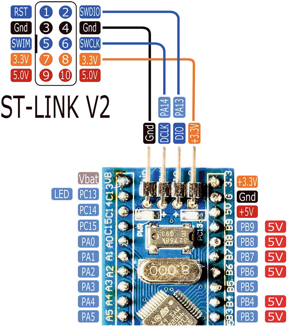
Figure 3-6 ST-LINK V2 programmer hookup to STM32F103C8T6 device. Check the connections on the device you have, assome ST-Link programmers are different.
With the programmer hooked up according to Figure 3-6, check your boot-0 and boot-1 jumpers located beside the Reset button. These should appear as they do in Figure 3-1 (with both jumpers close to the side marked “0”).
Plug your ST-Link V2 programmer into a USB port or use a USB extension cable. Once you do this, the power LED should immediately light. Also, the PC13 LED should also blink if your unit still has the blink program in it. Figure 3-7 illustrates the setup.
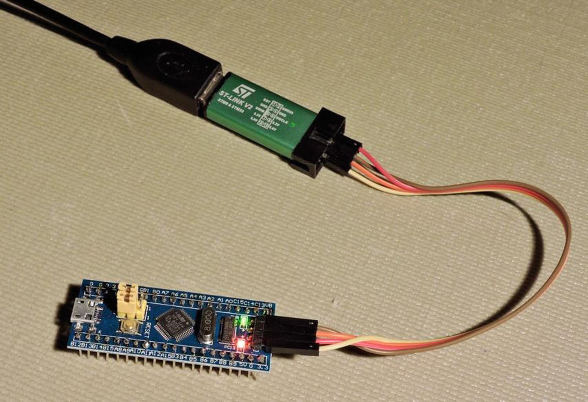
Figure 3-7 ST-Link V2 programmer using a USB extension cable, hooked up to the STM32F103C8T6 using DuPont wires
From your desktop, run the st-info command as follows:
$ st-info --probe
Found 1 stlink programmers
 serial: 493f6f06483f53564554133f
openocd: "x49x3fx6fx06x48x3fx53x56x45x54x13x3f"
  flash: 131072 (pagesize: 1024)
   sram: 20480
 chipid: 0x0410
  descr: F1 Medium-density device
The st-info command should find your ST-Link V2 programmer and the STM32F103C8T6 attached to it. The successful result should be similar to mine shown. Notice that the CPU serial number is reported along with the SRAM (20K). The amount of flash memory reported here is 128K, but you might see 64K instead. It will probably support 128K anyway.
st-flash Utility
Let’s now look at how you can use the st-flash utility to read (save), write (program), or erase your STM32 device.
Read STM32
Saving memory content from your device to a file will allow you to restore the original programming, should you need it later. The following example reads from your device’s flash memory, starting at address 0x80000000, and saves 0x1000 (4K) worth of data to a file named saved.img. Unless otherwise stated, the C programming 0x prefix convention will be used to indicate hexadecimal numbers in this book:
$ st-flash read ./saved.img 0x8000000 0x1000
st-flash 1.3.1-9-gc04df7f-dirty
2017-07-29T09:54:02 INFO src/common.c: Loading device parameters....
2017-07-29T09:54:02 INFO src/common.c: Device connected is:
     F1 Medium-density device, id 0x20036410
2017-07-29T09:54:02 INFO src/common.c: SRAM size: 0x5000 bytes (20 KiB),
     Flash: 0x20000 bytes (128 KiB) in pages of 1024 bytes
To check the content of the saved image file, use the hexedit utility (you may need to use your package manager to install it on your desktop):
$ hexedit saved.imgTo get help while in the utility, press F1. You can use Control-V to scroll down a page at a time. Use Control-C to exit out to the command line.
Examining the file, you should see hexadecimal content until about offset 0x4EC. From that point on, you may see hexadecimal 0xFF bytes, representing unwritten (erased) flashed memory. If you see nothing but zeros or 0xFF bytes, then something is wrong. Make sure you include the 0x prefix on the address and size arguments of the command.
If you don’t see a bunch of 0xFF bytes at the end of the saved image, it may be that you need to save a larger-sized image.
Write Image
Writing flash memory is the reverse of reading, of course. A saved memory image can be “flashed” by use of the write subcommand using st-flash. Note that we omit the size argument for this command. For this example, we write it back to the same address:
$ st-flash write ./saved.img 0x8000000
st-flash 1.3.1-9-gc04df7f-dirty
2017-07-29T10:00:39 INFO src/common.c: Loading device parameters....
2017-07-29T10:00:39 INFO src/common.c: Device connected is:
     F1 Medium-density device, id 0x20036410
2017-07-29T10:00:39 INFO src/common.c: SRAM size: 0x5000 bytes (20 KiB),
     Flash: 0x20000 bytes (128 KiB) in pages of 1024 bytes
2017-07-29T10:00:39 INFO src/common.c: Ignoring 2868 bytes of 0xff
     at end of file
2017-07-29T10:00:39 INFO src/common.c: Attempting to write 1228 (0x4cc)
     bytes to stm32 address: 134217728 (0x8000000)
Flash page at addr: 0x08000400 erased
2017-07-29T10:00:39 INFO src/common.c: Finished erasing 2 pages of 1024
     (0x400) bytes
2017-07-29T10:00:39 INFO src/common.c: Starting Flash write for
     VL/F0/F3 core id
2017-07-29T10:00:39 INFO src/flash_loader.c: Successfully loaded flash
     loader in sram
  1/1 pages written
2017-07-29T10:00:39 INFO src/common.c: Starting verification of write
     complete
2017-07-29T10:00:39 INFO src/common.c: Flash written and verified!
     jolly good!
This operation will restore your saved blink image file to the flash memory in your device. It may start to blink immediately. Otherwise, press the Reset button to force a restart.
Erase Flash
There may be times when you want to force a full erasure of the device. Perhaps you want to donate your device to a friend and want to eliminate your last experiment:
$ st-flash erase
st-flash 1.3.1-9-gc04df7f-dirty
2017-07-29T10:06:17 INFO src/common.c: Loading device parameters....
2017-07-29T10:06:17 INFO src/common.c: Device connected is:
     F1 Medium-density device, id 0x20036410
2017-07-29T10:06:17 INFO src/common.c: SRAM size: 0x5000 bytes (20 KiB),
     Flash: 0x20000 bytes (128 KiB) in pages of 1024 bytes
Mass erasing
After this operation completes, your device should be fully erased. It should also stop blinking. For fun, try now to restore the image and reset.
Summary
This chapter provided important information about powering options. This is critical because failures in this area can lead to permanent damage. By now, you have plugged in your unit and verified that it is functional with the included blink program. Then, you confirmed that the programmer and the device to be programmed are both functional using the st-link command. Finally, you learned how to use the st-flash utility to read, write, and erase flash memory on the device.