
Until this point, there’s been an elephant in the room. We’ve configured and used various clocks without saying too much about them. Now is a good time to reveal some of the clock components that have been lurking in the shadows.
While asynchronous logic circuit designs exist, most microprocessors use one or more clocks. The STM32 series is no exception. This series is highly configurable, adding somewhat to its software complexity. But this added flexibility allows the designer to reduce power requirements by turning off peripherals and clocks that are not required.
This chapter will examine the clocks that the STM32F103C8T6 supports and how to configure them. This information will make it possible for you to calculate the correct prescaler counts needed to produce correct baud rates and SPI clock rates, and to correctly feed timers. It will also give you inside information needed to take advantage of special clock features and avoid pitfalls.
In the Beginning
Many clocks can be derived from others, but there has to be one or more sources at the start of any chain. Within the STM32F103C8T6 there are a total of four independent clock sources, as follows
8 MHz RC oscillator (HSI)
4–16 MHz crystal/ceramic oscillator (HSE)
32.768 kHz crystal oscillator (LSE)
40 kHz RC oscillator (LSI)
Table 15-1 summarizes the notation used for the preceding oscillators, as well as some of their major characteristics. For example, it is shown that the HSE oscillator is driven by a crystal and enjoys good stability, while the HSI oscillator is driven by RC (resistor and capacitor) and has relatively poor stability.
Table 15-1 STM32 Oscillator Notation
Notation | Low/High Speed | Internal/External | Driven By | Stability |
|---|---|---|---|---|
LSI | Low speed | Internal | Resistor and Capacitor | Poor |
LSE | Low speed | External | Crystal | Good |
HSI | High speed | Internal | Resistor and Capacitor | Poor |
HSE | High speed | External | Crystal | Good |
RC Oscillators
A good question to ask is why provide RC oscillators if they are not that stable? For some applications, it may be enough that the MCU has a reasonable clock to execute instructions with. This saves the designer from having to supply a crystal and thus reduces the parts count.
Figure 15-1 illustrates the two crystals that are provided with the Blue Pill board. Notice the size of the 8.000 MHz crystal. Right beneath it in the photo is the 32.768 kHz crystal, which is housed in a rectangular blob of plastic. Relative to the MCU chip (above the 8 MHz crystal), these are large components.
The RC oscillator, as electronics folks know, consists of charging and discharging a capacitor through a resistor. The combination of capacitance and resistance determines the overall frequency. Creating capacitors inside of an IC (Integrated Circuit) presents challenges but is worth doing for chip buyers who want to reduce external components.
Note that the only STM32 RC oscillators provided are internal oscillators. Otherwise, resistors and capacitors would need to be supplied externally.

Figure 15-1 8 MHz crystal and 32.768 kHz crystal below it
Crystal Oscillators
Crystal oscillators are far more accurate and stable than the RC oscillator. However, they have the disadvantage that an external crystal must be supplied and wired up to the MCU chip. Figure 15-1 illustrates the two crystals found on the Blue Pill PCB, with the 8 MHz crystal used by the HSE oscillator. The 32.768 kHz crystal drives the LSE oscillator.
Oscillator Power
The higher rate at which the oscillator switches between low and high signal levels means additional current consumption. Every time the oscillator switches from low to high electrons have to be pushed into the circuit, thus requiring current flow (charging). When the oscillator switches from high to low, electrons have to be drawn out of the circuit and drained to ground (discharging). All of this requires energy.
It comes as no surprise then, if you do this charging and discharging more frequently in a given second, then more overall current is consumed. This is why so much attention is given to the clock design in the STM32 platform.
For some applications where the system is battery powered and the execution time is less important, it makes sense to use a lower-speed oscillator. If, on the other hand, the application is powered from a desktop over USB and speed is the dominant requirement, then higher oscillator rates are preferred.
Another selection criterion is accuracy. If you implement a serial link between different units, then you need to have an accurate notion of the baud rate. Having choice provides designers with different trade-offs.
Real-time Clock
The HSE, LSE, or LSI clock can be chosen for the source of the RTCCLK (real-time clock). Table 15-2 summarizes the clock configurations available. Note that the divisor is hardwired as 128 when the HSE clock is chosen.
Table 15-2 Real-time Clock Sources When HSE Is 8 MHz
Oscillator Source | Source Frequency | Divisor | Resulting Frequency |
|---|---|---|---|
HSE | 8.000 MHz | 128 | 62.5 kHz |
LSE | 32.768 kHz | 1 | 32.768 kHz |
LSI | 40 kHz | 1 | 40 kHz |
Watchdog Clock
The independent watchdog (IWDG) is hard wired to the LSI 40-kHz clock.
System Clock (SYSCLK)
The most interesting category of basic clock configuration is the system clock, from which other important clocks are derived. The SYSCLK can only be sourced from two of the four clock sources:
HSI (RC), 8 MHz
HSE (crystal), 4–16 MHz (8 MHz on Blue Pill)
There is one additional source that is derived from a phase-locked loop (PLL), which multiplies the frequency of the HSI or HSE clock input. When the source for the PLL is the HSI clock, the input is first divided by two. Table 15-3 provides a convenient table of values when HSI is used.
Table 15-3 System Clock Derived from HSI and PLL
Source | Frequency | PLL Multiplier | Resulting Frequency |
|---|---|---|---|
HSI | 8 MHz | No PLL | 8 MHz |
HSI | 8 MHz ÷ 2 | 2 | 8 MHz |
HSI | 8 MHz ÷ 2 | 3 | 12 MHz |
HSI | 8 MHz ÷ 2 | 4 | 16 MHz |
HSI | 8 MHz ÷ 2 | 5 | 20 MHz |
HSI | 8 MHz ÷ 2 | 6 | 24 MHz |
HSI | 8 MHz ÷ 2 | 7 | 28 MHz |
HSI | 8 MHz ÷ 2 | 8 | 32 MHz |
HSI | 8 MHz ÷ 2 | 9 | 36 MHz |
HSI | 8 MHz ÷ 2 | 10 | 40 MHz |
HSI | 8 MHz ÷ 2 | 11 | 44 MHz |
HSI | 8 MHz ÷ 2 | 12 | 48 MHz |
HSI | 8 MHz ÷ 2 | 13 | 52 MHz |
HSI | 8 MHz ÷ 2 | 14 | 56 MHz |
HSI | 8 MHz ÷ 2 | 15 | 60 MHz |
HSI | 8 MHz ÷ 2 | 16 | 64 MHz |
When the HSE is the chosen clock source, the calculation changes to the values shown in Table 15-4. The input to the PLL can use either the HSE divided by two (HSE ÷ 2) or not divided (HSE ÷ 1). The maximum usable system clock is 72 MHz.
Table 15-4 System Clock Derived from HSE and PLL
Source | Frequency | PLL Multiplier | HSE ÷ 2 | HSE ÷ 1 |
|---|---|---|---|---|
HSE | 8.000 MHz | No PLL | 8 MHz | 8 MHz |
HSE | 8.000 MHz | 2 | 8 MHz | 16 MHz |
HSE | 8.000 MHz | 3 | 12 MHz | 24 MHz |
HSE | 8.000 MHz | 4 | 16 MHz | 32 MHz |
HSE | 8.000 MHz | 5 | 20 MHz | 40 MHz |
HSE | 8.000 MHz | 6 | 24 MHz | 48 MHz |
HSE | 8.000 MHz | 7 | 28 MHz | 56 MHz |
HSE | 8.000 MHz | 8 | 32 MHz | 64 MHz |
HSE | 8.000 MHz | 9 | 36 MHz | 72 MHz |
HSE | 8.000 MHz | 10 | 40 MHz | over limit |
HSE | 8.000 MHz | 11 | 44 MHz | over limit |
HSE | 8.000 MHz | 12 | 48 MHz | over limit |
HSE | 8.000 MHz | 13 | 52 MHz | over limit |
HSE | 8.000 MHz | 14 | 56 MHz | over limit |
HSE | 8.000 MHz | 15 | 60 MHz | over limit |
HSE | 8.000 MHz | 16 | 64 MHz | over limit |
Figure 15-2 provides a slightly simplified diagram of the system clock tree up to the point of the SYSCLK. The asterisks identify what is normally configured for the Blue Pill STM32F103C8T6.
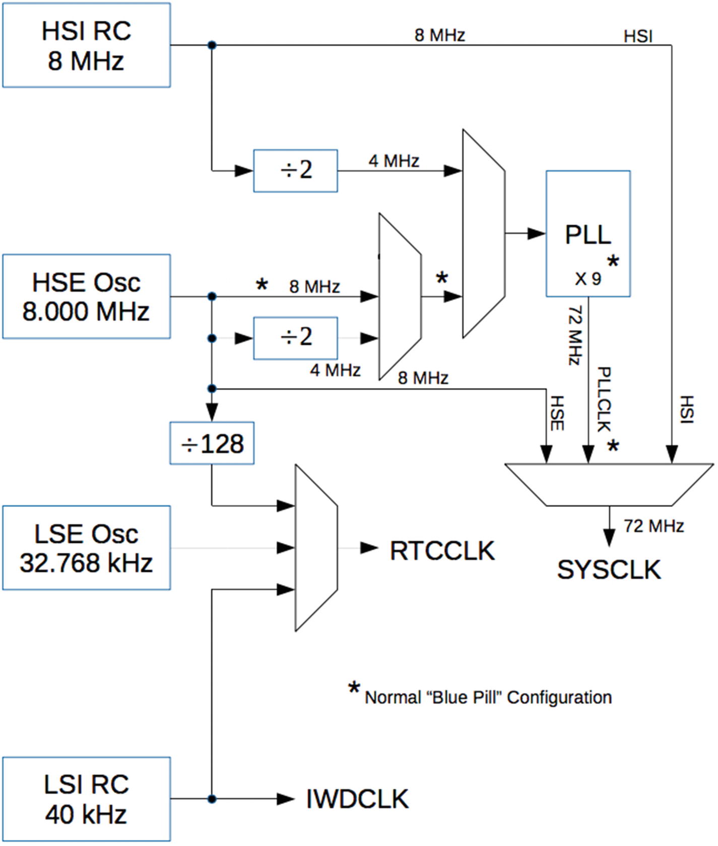
Figure 15-2 Simplified summary of clock tree up to the point of SYSCLK
SYSCLK and USB
If you’re not using USB, you can ignore this issue. But when USB support is required, your choices are limited, as outlined in Table 15-5. The USB prescaler must be set so that the USBCLK is 48 MHz.
Table 15-5 Valid Clock Configurations when USB Is Used
SYSCLK Frequency | USB Divisor | Resulting USB Clock |
|---|---|---|
72 MHz | ÷ 1.5 | 48 MHz |
48 MHz | ÷ 1 | 48 MHz |
AHB Bus
Throughout the ST Microelectronics document RM0008, which describes the STM32 series, references to AHB are made without ever explaining what it is. So, what is the AHB anyway? Wikipedia helps with this: 1
The ARM Advanced Microcontroller Bus Architecture (AMBA) is an open-standard, on-chip interconnect specification for the connection and management of functional blocks in system-on-a-chip (SoC) designs. . . . AMBA was introduced by ARM in 1996. The first AMBA buses were Advanced System Bus (ASB) and Advanced Peripheral Bus (APB). In its second version, AMBA 2 in 1999, ARM added AMBA Hi gh-performance Bus (AHB) that is a single clock-edge protocol.
There we have it—AHB is the AMBA high-performance bus. Within the STM32 family, the AHB has a prescaler that uses the SYSCLK as the input. Assuming that the SYSCLK is 72 MHz, Table 15-6 summarizes the AHB choices.
Table 15-6 STM32F103C8T6 AHB Frequencies with a 72 MHz SYSCLK
Bit Value | Divisor | Resulting Frequency |
|---|---|---|
0xxx | SYSCLK not divided | 72 MHz |
1000 | SYSCLK divided by 2 | 36 MHz |
1001 | SYSCLK divided by 4 | 18 MHz |
1010 | SYSCLK divided by 8 | 9 MHz |
1011 | SYSCLK divided by 16 | 4.5 MHz |
1100 | SYSCLK divided by 64 | 1.125 MHz |
1101 | SYSCLK divided by 128 | 562.5 kHz |
1110 | SYSCLK divided by 256 | 281.25 kHz |
1111 | SYSCLK divided by 512 | 140.625 kHz |
Starting from SYSCLK, Figure 15-3 illustrates why this is called a clock tree. From the SYSCLK signal, many other clocks are derived from configured divisors and enables.
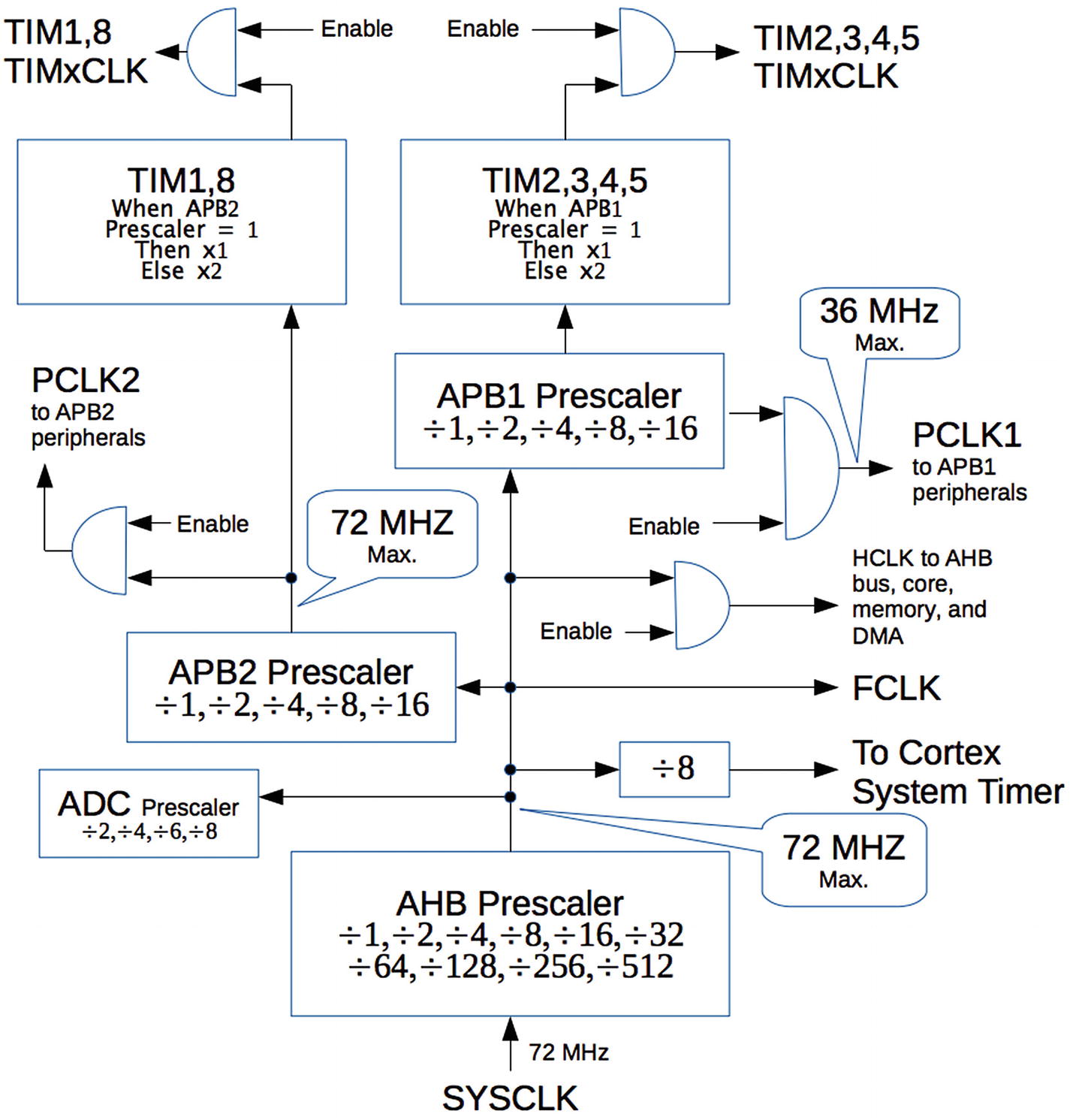
Figure 15-3 Clock tree starting from SYSCLK
rcc_clock_setup_in_hse_8mhz_out_72mhz( )
In most of the demos presented in this book, the following libopencm3 routine is used at the start of the main program:
rcc_clock_setup_in_hse_8mhz_out_72mhz();To help us understand specifically what that is doing, Listing 15-1 illustrates the libopencm3 function code for it.
Listing 15-1 The Function rcc_clock_setup_in_hse_8mhz_out_72mhz( )
0911: void rcc_clock_setup_in_hse_8mhz_out_72mhz(void)
0912: {
0913:   /* Enable internal high-speed oscillator. */
0914:   rcc_osc_on(RCC_HSI);
0915:   rcc_wait_for_osc_ready(RCC_HSI);
0916:
0917:   /* Select HSI as SYSCLK source. */
0918:   rcc_set_sysclk_source(RCC_CFGR_SW_SYSCLKSEL_HSICLK);
0919:
0920:   /* Enable external high-speed oscillator 8MHz. */
0921:   rcc_osc_on(RCC_HSE);
0922:   rcc_wait_for_osc_ready(RCC_HSE);
0923:   rcc_set_sysclk_source(RCC_CFGR_SW_SYSCLKSEL_HSECLK);
0924:
0925:   /*
0926:    * Set prescalers for AHB, ADC, ABP1, ABP2.
0927:    * Do this before touching the PLL (TODO: why?).
0928:    */
0929:   rcc_set_hpre(RCC_CFGR_HPRE_SYSCLK_NODIV);/* Set. 72MHz Max. 72MHz */
0930:   rcc_set_adcpre(RCC_CFGR_ADCPRE_PCLK2_DIV8);/*Set. 9MHz Max. 14MHz */
0931:   rcc_set_ppre1(RCC_CFGR_PPRE1_HCLK_DIV2); /* Set. 36MHz Max. 36MHz */
0932:   rcc_set_ppre2(RCC_CFGR_PPRE2_HCLK_NODIV);/* Set. 72MHz Max. 72MHz */
0933:
0934:   /*
0935:    * Sysclk runs with 72MHz -> 2 waitstates.
0936:    * 0WS from 0-24MHz
0937:    * 1WS from 24-48MHz
0938:    * 2WS from 48-72MHz
0939:    */
0940:   flash_set_ws(FLASH_ACR_LATENCY_2WS);
0941:
0942:   /*
0943:    * Set the PLL multiplication factor to 9.
0944:    * 8MHz (external) * 9 (multiplier) = 72MHz
0945:    */
0946:   rcc_set_pll_multiplication_factor(RCC_CFGR_PLLMUL_PLL_CLK_MUL9);
0947:
0948:   /* Select HSE as PLL source. */
0949:   rcc_set_pll_source(RCC_CFGR_PLLSRC_HSE_CLK);
0950:
0951:   /*
0952:    * External frequency undivided before entering PLL
0953:    * (only valid/needed for HSE).
0954:    */
0955:   rcc_set_pllxtpre(RCC_CFGR_PLLXTPRE_HSE_CLK);
0956:
0957:   /* Enable PLL oscillator and wait for it to stabilize. */
0958:   rcc_osc_on(RCC_PLL);
0959:   rcc_wait_for_osc_ready(RCC_PLL);
0960:
0961:   /* Select PLL as SYSCLK source. */
0962:   rcc_set_sysclk_source(RCC_CFGR_SW_SYSCLKSEL_PLLCLK);
0963:
0964:   /* Set the peripheral clock frequencies used */
0965:   rcc_ahb_frequency = 72000000;
0966:   rcc_apb1_frequency = 36000000;
0967:   rcc_apb2_frequency = 72000000;
0968: }
The basic steps used are the following:
The HSI oscillator is turned on and waits for it to become ready (lines 914 to 915).
Selects the HSI oscillator as the SYSCLK source (line 918).
The HSE (8 MHz crystal oscillator) is enabled in line 921, and the code waits until it is ready (line 922).
The SYSCLK is then switched to use the HSE clock (line 923). Note that this is not the PLL yet, so at this point the SYSCLK is 8.000 MHz as determined by the crystal.
The AHB is set to use no divisor in its prescaler (line 929), resulting in an input AHB clock of 72 MHz after the PLL is selected (later) as the clock source.
The ADC prescaler is configured with a divisor of 8 (line 930), which results in a frequency of 9 MHz (after switch to the PLL). As the comment indicates, it must not exceed 14 MHz.
The prescaler for APB1 (Advanced Peripheral Bus 1) is set to divide by 2, resulting in an APB1 clock of 36 MHz after switch to the PLL (line 931). This is the maximum frequency for this bus.
The prescaler for APB2 is set to use no divisor, resulting in an APB2 frequency of 72 MHz when switched later to use the PLL (line 932). This is also the maximum frequency for APB2.
Since the SYSCLK runs at 72 MHz, there must be two wait cycles inserted for each flash memory access (line 940).
The PLL is now set with a multiplier of 9 to set its output clock to 72 MHz (line 946).
Line 955 removes any ÷ 2 setting for HSE entering the PLL that might be set.
Finally, line 962 selects the PLL as the SYSCLK source. This increases the SYSCLK from 8 to 72 MHz, with the AHB bus now operating at 72 MHz, APB1 running at 36 MHz, and APB2 running at 72 MHz.
Lines 965 to 967 set global values rcc_ahb_frequency, rcc_apb1_frequency and rcc_apb2_frequency for application use.
The globals are defined in rcc.h and are defined as follows:
#include <libopencm3/stm32/rcc.h>extern uint32_t rcc_ahb_frequency;extern uint32_t rcc_apb1_frequency;extern uint32_t rcc_apb2_frequency;
From this, you can see that there is quite a bit that must be done at startup to make sure that no clocks falter or fail.
APB1 Peripherals
Each peripheral connected to the APB1 bus in the Blue Pill device receives a 36 MHz clock (unless otherwise configured). Each peripheral, however, has a private AND-gate to enable/disable this clock in order to save power. To enable the receipt of the clock, the peripheral must enable it. For example, the CAN peripheral must enable the clock for the peripheral itself. The same applies to APB1 timer peripherals.
APB2 Peripherals
Like the APB1 peripherals, each peripheral attached to the APB2 bus must enable/disable the receipt of their own 72 MHz clock. This also applies to APB2 timer peripherals.
Timers
Special mention is made of timers here because there is a not-so-obvious wrinkle in their configuration. APB1 and APB2 timers have a prescaler, allowing their bus clocks to be divided down for a lower frequency. The exception, however, is that when the APB1/APB2 prescaler is set to one, the bus frequency is multiplied by two!
Note
When a timer prescaler is set to 1, the output of the prescaler is a bus frequency times 2!
rcc_set_mco( )
The libopencm3 library provides a function named rcc_set_mco() to configure a clock output on GPIO PA8. The valid macro values passed as an argument are described in Table 15-7.
rcc_set_mco(macro);Table 15-7 Valid Arguments to rcc_set_mco( )
Macro Name | Value | Description |
|---|---|---|
RCC_CFGR_MCO_NOCLK | 0 x 0 | No clock to MCO (disconnected) |
RCC_CFGR_MCO_SYSCLK | 0 x 4 | SYSCLK to MCO |
RCC_CFGR_MCO_HSI | 0 x 5 | HSI to MCO |
RCC_CFGR_MCO_HSE | 0 x 6 | HSE to MCO |
RCC_CFGR_MCO_PLL_DIV2 | 0 x 7 | PLL ÷ 2 to MCO |
Calling the routine rcc_set_mco() by itself is not enough. The GPIO PA8 must be configured for alternate function I/O:
rcc_periph_clock_enable(RCC_GPIOA);
gpio_set_mode(GPIOA,
    GPIO_MODE_OUTPUT_50_MHZ,
    GPIO_CNF_OUTPUT_ALTFN_PUSHPULL, // ALTFN
    GPIO8);                         // PA8=MCO
HSI Demo
The example code for the HSI clock demo is located here:
$ cd ~/stm32f103c8t6/hsi
$ make clobber
$ make
$ make flash
Note that this demo does not use FreeRTOS. Its code is very basic and simply arranges to have the HSI clock brought out to GPIO pin PA8. Listing 15-2 shows the main program responsible.
Listing 15-2 The hsi.c Demonstration Program
0010: int
0011: main(void) {
0012:
0013:   // LED Configuration:
0014:   rcc_periph_clock_enable(RCC_GPIOC);
0015:   gpio_set_mode(GPIOC,GPIO_MODE_OUTPUT_2_MHZ,
0016:             GPIO_CNF_OUTPUT_PUSHPULL,GPIO13);
0017:   gpio_clear(GPIOC,GPIO13);    // LED Off
0018:
0019:   // MCO Configuration:
0020:   rcc_periph_clock_enable(RCC_GPIOA);
0021:   gpio_set_mode(GPIOA,
0022:       GPIO_MODE_OUTPUT_50_MHZ,
0023:       GPIO_CNF_OUTPUT_ALTFN_PUSHPULL,
0024:       GPIO8);             // PA8=MCO
0025:
0026:   rcc_set_mco(RCC_CFGR_MCO_HSI);
0027:
0028:   gpio_set(GPIOC,GPIO13); // LED On
0029:   for (;;);
0030:   return 0;
0031: }
Aside from configuring the LED PC13, the main elements are as follows:
The GPIOA peripheral clock is enabled in line 20.
The GPIOA to which pin PA8 is configured for output (max 50 MHz, line 22) is an alternate function (line 23) in push/pull mode.
The HSI clock is directed to PA8 in line 26.
After flashing the STM32, you should be able to see the HSI clock on PA8 with a scope or DSO as soon as power is applied or after reset (Figure 15-4). From the figure, you can see that the HSI clock is near 8 MHz.
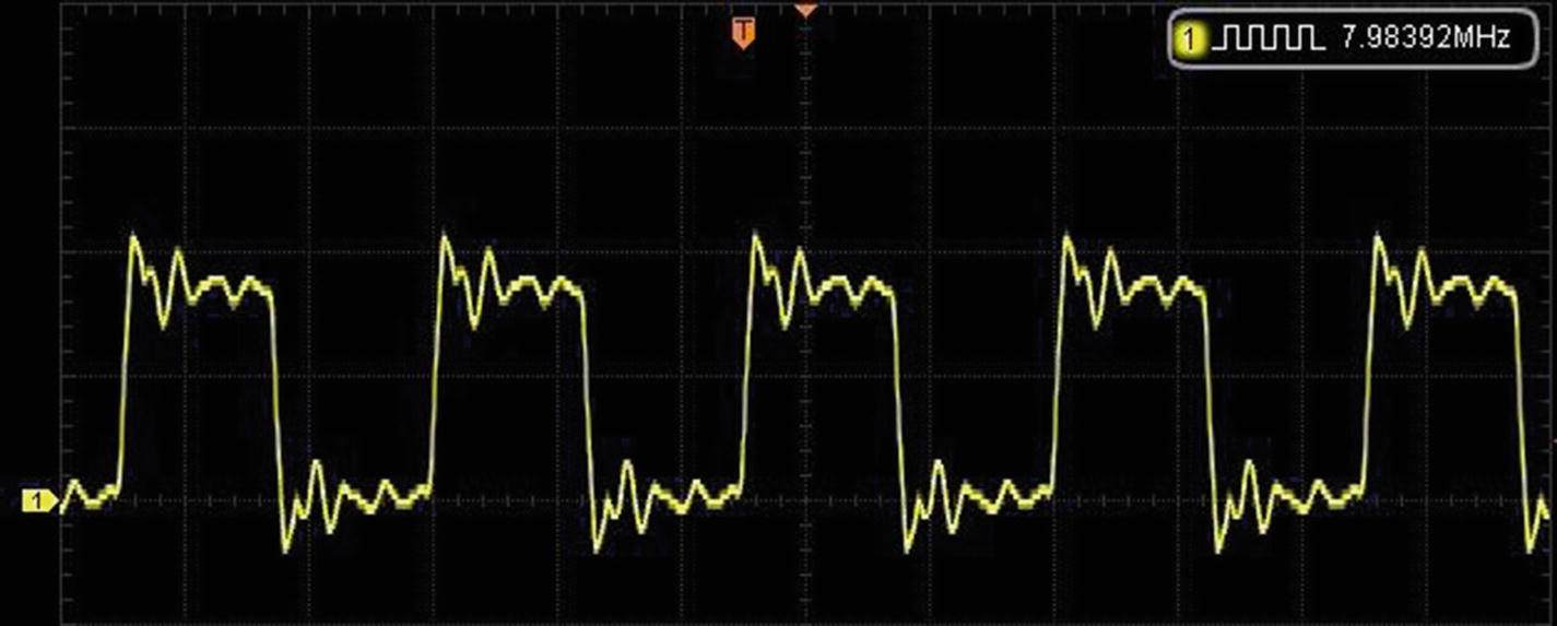
Figure 15-4 The HSI MCO trace
HSE Demo
The example code for the HSE clock demo is located here:
$ cd ~/stm32f103c8t6/hse
$ make clobber
$ make
$ make flash
Note that this demo also does not use FreeRTOS. Its code is basic and simply arranges to have the HSE clock brought out to GPIO pin PA8. The only difference between this demo program and the HSI demo is one line:
rcc_set_mco(RCC_CFGR_MCO_HSE);After flashing the STM32, you should be able to see the HSE clock on PA8 with a scope or DSO as soon as power is applied (Figure 15-5). In the figure, the frequency is more accurate to 8 MHz.
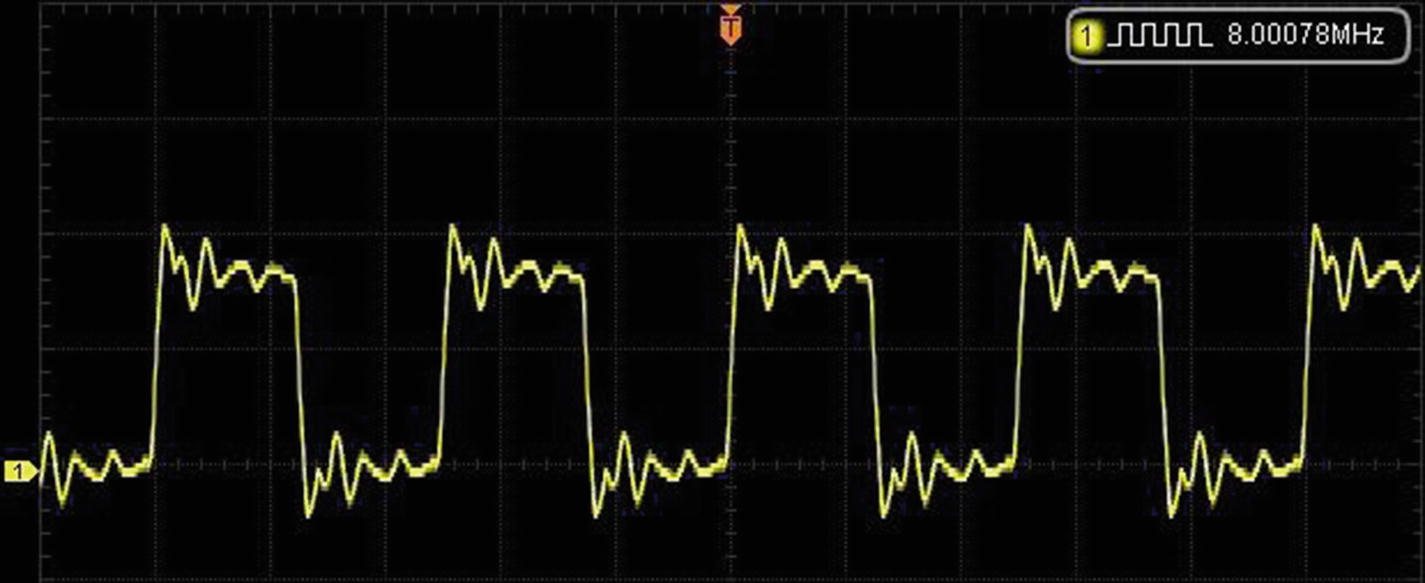
Figure 15-5 The HSE MCO trace (note how similar this is to Figure 15-4)
PLL ÷ 2 Demo
The example code for the PLL ÷ 2 clock demo is located here:
$ cd ~/stm32f103c8t6/mco_pll2
$ make clobber
$ make
$ make flash
Note again that this demo also does not use FreeRTOS. Its code is basic and simply arranges to have the PLL ÷ 2 clock brought out to GPIO pin PA8. The only difference between this demo program and the HSE demo is one line:
rcc_set_mco(RCC_CFGR_MCO_PLL_DIV2);Having the PLL ÷ 2 clock sent out to PA8 is helpful because the GPIO pin is limited to driving 50 MHz. You could attempt to send 72 MHz out, but the signal would be badly degraded and perhaps stress the active components involved. But 36 MHz is well within the acceptable performance range.
After flashing the STM32, you should be able to see the PLL ÷ 2 clock on PA8 with a scope or DSO as soon as power is applied. Notice that the frequency shown is near 36 MHz, as expected (72 MHz ÷ 2), in Figure 15-6.

Figure 15-6 The PLL ÷ 2 MCO trace
Summary
In this chapter, the overview of the clock-tree system was presented, starting with the main clock sources: HSI and HSE for the system clock, and HSE, LSE, and LSI for the real-time clock. Clock LSI was also used by the watchdog timer.
The next main category of clocks stem from the system clock. The system clock is able to employ the use of the PLL, which is capable of multiplying its input clock up to 72 MHz. From the system clock, an AHB clock is derived. Then, from the AHB clock are derived APB1 and APB2 clocks.
Finally, it was noted that each peripheral needing a clock has its own gate that it must enable in order to use a given clock. This design saves power by leaving unneeded clocks disabled.
The HSI, HSE, and PLL ÷ 2 demos illustrated how to check a clock that is otherwise internal and unseen. It is also possible that a clock placed on PA8 may have its application to external peripherals needing an input clock.
Bibliography
“Advanced Microcontroller Bus Architecture.” Wikipedia. December 16, 2017. Accessed December 29, 2017. https://en.wikipedia.org/wiki/Advanced_Microcontroller_Bus_Architecture