
Embedded computing often needs to convert an analog signal level into a digital form for analysis. One application is measuring temperature by the voltage developed across a semiconductor. It is no surprise then that the STM32 platform has both an analog-to-digital converter (ADC) and a built-in channel to the ADC for measuring temperature.
This chapter’s demonstration project will illustrate how to use the libopencm3 routines to access the ADC peripheral, reading analog channels PA0 and PA1, in addition to reading the chip temperature and its internal reference voltage.
STM32F103C8T6 Resources
The STM32F103C8T6 sports two ADC controllers, specified by the following libopencm3 macro names:
ADC1 — 12-bit Analog Digital Controller 1 with 18 input channels
ADC2 — 12-bit Analog Digital Controller 2 with 16 input channels
These each support 16 analog input channels. ADC1 can also access internal levels for temperature and a reference voltage V ref .
The ADC peripheral also includes a programmable prescaler that establishes the conversion rate. The input to the prescaler is the PCLK2 (same as APB2) clock. Since our demo initializes with the call
rcc_clock_setup_in_hse_8mhz_out_72mhz();this results in the APB2 frequency being established as
rcc_apb2_frequency = 72000000;or 72 MHz. The ADC input clock must not exceed 14 MHz, so this limits us to the divisor 6, generating a clock of 72 ÷ 6 = 12 MHz.
Demonstration
There is no schematic for this demonstration since all is provided by the onboard ADC peripheral. The only external connections of interest are the analog inputs PA0 and PA1. However, a schematic will be provided later for how to hook up a potentiometer to generate voltages that can be sensed. This chapter is mostly about how to arrange the software to operate the ADC peripheral.
Caution
GPIO inputs PA0 and PA1 are not 5-volt tolerant and should only receive voltages between zero and +3.3 volts.
The software for this chapter is found at the following directory:
$ cd ~/stm32f103c8t6/rtos/adcChange to that subdirectory and rebuild the project from scratch:
$ make clobber$ make$ make flash
Tip
It should not be necessary to change the Boot-0 jumper to reflash the STM32 for this project, except perhaps the first time.
Analog Inputs PA0 and PA1
In the main() program, the ADC peripheral and its GPIOs are initialized. The first step configures the analog inputs, as follows:
0087: rcc_periph_clock_enable(RCC_GPIOA); // Enable GPIOA for ADC0088: gpio_set_mode(GPIOA,0089: GPIO_MODE_INPUT,0090: GPIO_CNF_INPUT_ANALOG, // Analog mode0091: GPIO0|GPIO1); // PA0 & PA1
As usual, the clock for GPIO is enabled in line 87. Lines 88 to 91 configure GPIOs PA0 and PA1 for analog input. Notice that the value GPIO_CNF_INPUT_ANALOG is used to configure the GPIO input. This permits a varying voltage to reach the ADC instead of a digital high/low value.
ADC Peripheral Configuration
The main complexity of this demonstration is correctly configuring the ADC peripheral. The STM32 has a dizzying array of options in this area. Listing 14-1 illustrates the configuration used by this demo. All source code presented in this chapter is found in file main.c.
The ADC peripheral’s clock needs to be turned on, which line 103 accomplishes. The ADC peripheral’s power (not its clock) is disabled in line 104 for initialization.
Listing 14-1 ADC Configuration
0102: // Initialize ADC:0103: rcc_peripheral_enable_clock(&RCC_APB2ENR,RCC_APB2ENR_ADC1EN);0104: adc_power_off(ADC1);0105: rcc_peripheral_reset(&RCC_APB2RSTR,RCC_APB2RSTR_ADC1RST);0106: rcc_peripheral_clear_reset(&RCC_APB2RSTR,RCC_APB2RSTR_ADC1RST);0107: rcc_set_adcpre(RCC_CFGR_ADCPRE_PCLK2_DIV6);// Set. 12MHz, Max. 14MHz0108: adc_set_dual_mode(ADC_CR1_DUALMOD_IND); // Independent mode0109: adc_disable_scan_mode(ADC1);0110: adc_set_right_aligned(ADC1);0111: adc_set_single_conversion_mode(ADC1);0112: adc_set_sample_time(ADC1,ADC_CHANNEL_TEMP,ADC_SMPR_SMP_239DOT5CYC);0113: adc_enable_temperature_sensor();0114: adc_power_on(ADC1);0115: adc_reset_calibration(ADC1);0116: adc_calibrate_async(ADC1);0117: while (adc_is_calibrating(ADC1));
Lines 105 and 106 reset the ADC further. These are separate calls because of the different registers involved.
ADC Prescaler
Line 107 sets the ADC prescaler to operate at 12 MHz maximum. The ADC clock will function up to 14 MHz, but the divisor of 4 results in 18 MHz, which is clearly over the limit. If your application requires the highest possible ADC conversion rate, the only choice is to alter the CPU and other clocks first. Keep in mind that there are clock constraints affecting the USB controller, which may limit your options if USB is required.
ADC Modes
Lines 108 through 111 configure a series of different modes available. Line 108 allows ADC1 and ADC2 to be operated independently. Line 109 disables the scan-mode option, while line 110 configures the ADC to store the result right-justified in its register. Finally, line 111 configures the ADC to stop when a single conversion is completed:
0108: adc_set_dual_mode(ADC_CR1_DUALMOD_IND); // Independent mode0109: adc_disable_scan_mode(ADC1);0110: adc_set_right_aligned(ADC1);0111: adc_set_single_conversion_mode(ADC1);
Sample Time
Lines 112 and 113 establish the sample time to be used on the temperature and V ref channels:
0112: adc_set_sample_time(ADC1,ADC_CHANNEL_TEMP,ADC_SMPR_SMP_239DOT5CYC);0113: adc_set_sample_time(ADC1,ADC_CHANNEL_VREF,ADC_SMPR_SMP_239DOT5CYC);0114: adc_enable_temperature_sensor();
Each channel of the ADC can be sampled with a different number of clock cycles. The default is to have each conversion occur in 1.5 cycles (ADC_SMPR_SMP_1DOT5CYC). The total number of clock cycles is given by the following equation:![]()
In the case of line 112, the conversion time for temperature requires the following:
Since the ADC clock rate is 12 MHz, we know that the total time for conversion is as follows:
The default sample rate for a given channel is 1.5 cycles. Table 14-1 lists the sample rates that are available.
Table 14-1 ADC Sample Rates
libopencm3 Macro Name | Cycles | Total time (12 MHz ADC clock) |
|---|---|---|
ADC_SMPR_SMP_1DOT5CYC | 1.5 + 12.5 = 14 | 1.167 μs |
ADC_SMPR_SMP_7DOT5CYC | 7.5 + 12.5 = 20 | 1.667 μs |
ADC_SMPR_SMP_13DOT5CYC | 13.5 + 12.5 = 26 | 2.167 μs |
ADC_SMPR_SMP_28DOT5CYC | 28.5 + 12.5 = 41 | 3.417 μs |
ADC_SMPR_SMP_41DOT5CYC | 41.5 + 12.5 = 54 | 4.500 μs |
ADC_SMPR_SMP_55DOT5CYC | 55.5 + 12.5 = 68 | 5.667 μs |
ADC_SMPR_SMP_71DOT5CYC | 71.5 + 12.5 = 84 | 7.000 μs |
ADC_SMPR_SMP_239DOT5CYC | 239.5 + 12.5 = 252 | 21.00 μs |
Readying the ADC
Before the ADC controller is used, three more steps are required (from Listing 14-1):
0114: adc_power_on(ADC1);0115: adc_reset_calibration(ADC1);0116: adc_calibrate_async(ADC1);0117: while (adc_is_calibrating(ADC1));
Power is turned on by line 114, and calibration constants reset in line 115. Line 116 starts the calibration, while line 117 waits for this to complete. In the demonstration program this is all performed before the FreeRTOS scheduler is started.
Demonstration Run
Once the STM32 has been flashed with the demonstration code, plug in its USB cable and start minicom (again, “usb” is the file name that I used to save the USB comms parameters):
$ minicom usbWelcome to minicom 2.7OPTIONS:Compiled on Sep 17 2016, 05:53:15.Port /dev/cu.usbmodemWGDEM1, 12:38:28Press Meta-Z for help on special keysTemperature 24.72 C, Vref 1.19 Volts, ch0 1.92 V, ch1 0.00 VTemperature 24.72 C, Vref 1.19 Volts, ch0 1.94 V, ch1 0.00 VTemperature 24.72 C, Vref 1.19 Volts, ch0 1.97 V, ch1 0.00 VTemperature 24.72 C, Vref 1.19 Volts, ch0 1.98 V, ch1 0.00 V
Every 1.5 seconds a new line will be displayed, showing the following:
Internal STM32 temperature in °C (24.72 °C in the example)
Internal V ref value of the STM32 (1.19 volts in example)
Channel 0 voltage (1.92 volts in first example line)
Channel 1 voltage (0.00 volts in the example)
To test analog inputs A0 and A1, you can attach a jumper wire first to Gnd and then to your +3.3-volt supply. Do not apply voltages higher than that or negative voltages—this could result in permanent damage.
The session just shown had PA1 floating, while PA0 was grounded. If you now apply +3.3 volts to the PA0 input, the reported value should be close to +3.3 volts. I got 3.29 volts when I tried this. Repeat the grounding and +3.3-volt test on PA1, and the program should report identical results.
Reading ADC
With the ADC configured in the main() program, it is possible for the demo_task() function to read the analog voltages by channel, as follows:
0060: int adc0, adc1;...0068: adc0 = read_adc(0) * 330 / 4095;0069: adc1 = read_adc(1) * 330 / 4095;
To avoid floating point for speed and to reduce flash size, integer arithmetic is used here to compute voltages in variables adc0 and adc1. A 12-bit ADC result has 4096 possible steps, resulting in the returned result ranging from 0 to 4095. The result of the calculation when multiplied by 330 is volts times one hundred.
The software responsible for reading from the ADC is given in Listing 14-2.
Listing 14-2 Reading the ADC Results
0030: static uint16_t0031: read_adc(uint8_t channel) {0032:0033: adc_set_sample_time(ADC1,channel,ADC_SMPR_SMP_239DOT5CYC);0034: adc_set_regular_sequence(ADC1,1,&channel);0035: adc_start_conversion_direct(ADC1);0036: while ( !adc_eoc(ADC1) )0037: taskYIELD();0038: return adc_read_regular(ADC1);0039: }
Line 33 sets the sample time to 21 μs, and the sampling sequence is established in line 34. It specifies that one channel is to be sampled (argument 2), with the channel given by the list, starting with argument address &channel (this is a one-element list).
Line 35 launches the successive approximation ADC in line 35 and waits for completion in lines 36 and 37. Once again, taskYIELD() is called to allow other tasks to efficiently share the CPU time. Finally, line 38 fetches the conversion result and returns it to the caller.
Computing Temperature
The demo_task() makes the following call to acquire internal temperature:
0066: temp100 = degrees_C100();Listing 14-3 lists the function degrees_C100() .
Listing 14-3 The degrees_C100() Function
0044: static int0045: degrees_C100(void) {0046: static const int v25 = 143;0047: int vtemp;0048:0049: vtemp = (int)read_adc(ADC_CHANNEL_TEMP) * 3300 / 4095;0050:0051: return (v25 - vtemp) / 45 + 2500;// temp = (1.43 - Vtemp) / 4.5 + 25.000052: }
The STM32F103C8T6 documentation is very sketchy about this calculation. Since the PDF reference document (RM0008) applies to a whole family of STM32 devices, it is difficult to sort out the calculation needed by the Blue Pill device.
The information needed is available from the PDF found at:
http://www.st.com/resource/en/datasheet/stm32f103tb.pdf
For the STM32F103x8 and STM32F103xB series chips, look at the PDF’s Table 50. That table is made available as Table 14-2 in this chapter for your convenience.
As indicated in the source code, and derived from the PDF document, the temperature for the STM32F103C8T6 device is computed as follows: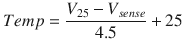
Table 14-2 Temperature Sensor Characteristics for STM32F103x8 and STM32F103xB Devices
Symbol | Parameter | Min | Typ | Max | Unit |
|---|---|---|---|---|---|
T L | V sense linearity with temperature | - | ±1 | ±2 | °C |
Avg_Slope | Average slope | 4.0 | 4.3 | 4.6 | mV/°C |
V 25 | Voltage at 25 °C | 1.34 | 1.43 | 1.52 | V |
t START | Startup time | 4 | - | 10 | μs |
T S_temp | ADC sampling time when reading the temperature | - | - | 17.1 | μs |
In Listing 14-3, you can see that the typical value of V25=1.43 (x 100) was used from Table 14-2. The value 45 comes from 4.5 for Avg_Slope (the value x 10). This seemed to better match for the device I was using and is in the range listed. But if you find the computed value to be high, try reducing the value 45 to 43 (representing the slope of 4.3).
Another value of interest is T S_temp , which is given as 17.1 μs. This is the sampling time performed by the testing that resulted in the tabled results. This is also the recommended sampling time found in RM0008.
When you don’t need the temperature reading or the V ref , you can save power consumption by turning them off, as follows:
adc_disable_temperature_sensor();The datasheet also includes this note about temperature:
The temperature sensor output voltage changes linearly with temperature. The offset of this line varies from chip to chip due to process variation (up to 45 °C from one chip to another).
The internal temperature sensor is more suited to applications that detect temperature variations instead of absolute temperatures. If accurate temperature readings are needed, an external temperature sensor part should be used.
Voltage Reference
ADC1 allows you to read an internal voltage V ref . This value can be used to calibrate the ADC to improve accuracy, with a typical value of 1.2 volts. Application Note AN2834 contains some very good information for those seeking the best available accuracy from the STM32 platform.
Analog Voltages
Reading 0 volts or +3.3 volts may not seem too exciting, so let’s improve upon that. You can generate any voltage in that range with the help of a potentiometer. While a range of values from about 1 kohm to 15 kohms should be suitable, it is best to use the low end of this range for stable readings.
Figure 14-1 illustrates the 10-kohm potentiometer (or simply “pot”) that I used for this experiment. If you’re purchasing one, get a linear pot rather than an audio-tapered pot. Audio-tapered pots vary logarithmically to make volume controls change with the sense of hearing. North American suppliers will use a “B” prefix like “B10K” to indicate linear, like the one shown in Figure 14-1.
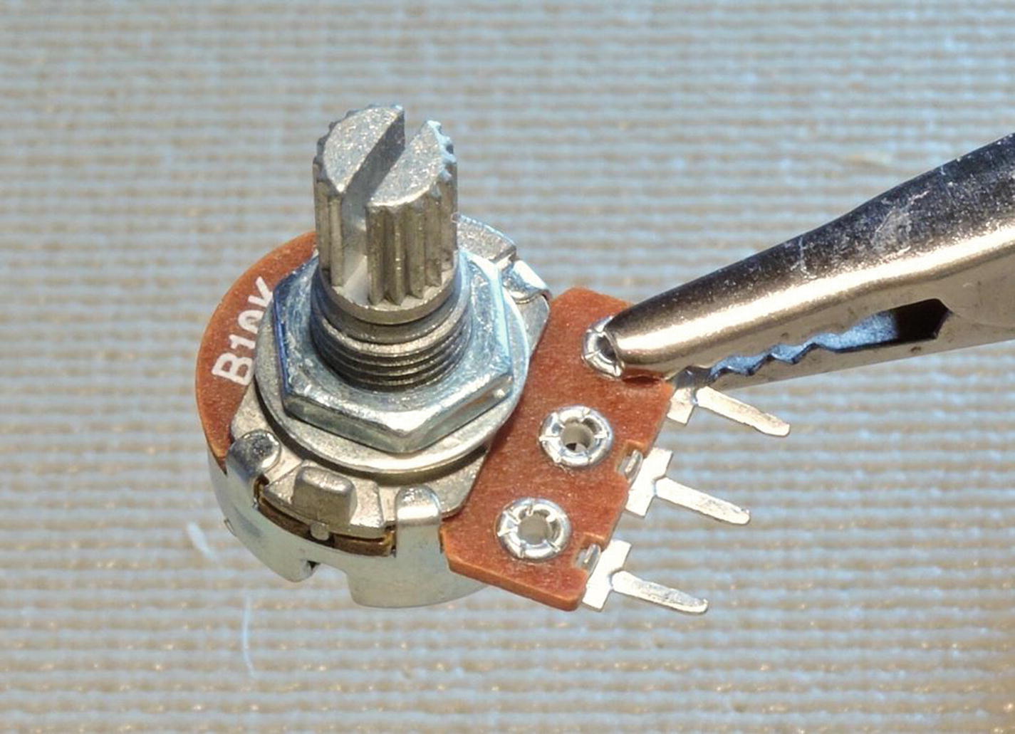
Figure 14-1 A linear 10-kohm potentiometer
The circuit is illustrated in Figure 14-2 . You can use just one pot if you lack a second. Be sure to wire the lugs at opposite ends of the pot to the supply and ground. The center lug is connected to the wiper inside the pot and should be wired to your ADC input PA0 or PA1.
With minicom connected, you can turn the pots counter-clockwise. If the voltage reads near +3.3 volts when turned counter-clockwise, reverse the connections on the outer lugs of the pot. Corrected, it should read near zero. When you turn the pot midway, you should be able to read about +1.5 volts, and fully clockwise should return readings near +3.3 volts.
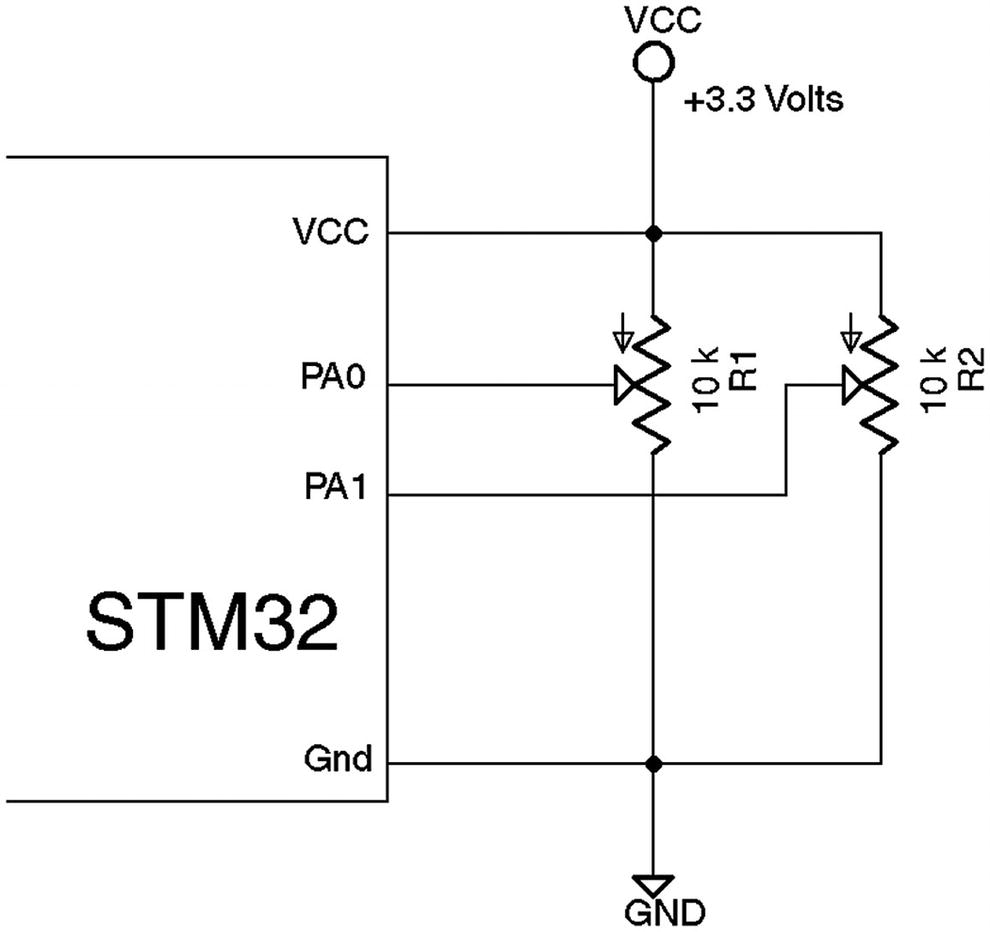
Figure 14-2 A pair of potentiometers wired to ADC inputs PA0 and PA1
Summary
The presented demo has just scratched the surface of what the STM32 ADC peripheral provides in the way of flexibility. In addition to single conversions, the ADC peripheral can be configured to use channel groups and perform scans. In addition to scanning any sequence of channels, it is also possible to have ADC values injected into the results. Finally, scanning and groups can include channels from peripherals ADC1 and ADC2.
This chapter gives you a simple place to start for ADC usage. Read chapter 11 of the STM32 reference manual RM0008 for the full extent of the ADC’s sampling capabilities. 1
Bibliography
STMicroelectronics. Accessed January 12, 2018. http://www.st.com/resource/en/reference_manual/cd00171190.pdf