
Chapter 4
Defect Structure in Low Stacking Fault Energy Nanomaterials
Abstract
In this chapter, the effect of low stacking fault energy (SFE) on a defect structure in nanomaterials is summarized. The low value of SFE leads to a large degree of dislocation dissociation into partials that hinder strongly the cross-slip and climb of dislocations. As a consequence, a relatively large dislocation density develops during severe plastic deformation of low SFE metallic materials. Additionally, the low SFE is accompanied by a small value of twin boundary energy resulting in a significant twinning activity during plastic deformation that alters grain-refinement mechanisms. Among the pure face-centered cubic metals, silver has the lowest SFE. Therefore, the effect of processing conditions and impurity content on dislocation density and twin-fault probability in ultrafine-grained (UFG) and nanocrystalline Ag is revealed and discussed in detail. In addition, the lattice defect structure in UFG alloys with low SFE is also studied. It is shown that the reduction of grain size increases the splitting distance between partials and the probability of occurrence of twinning in UFG and nanocrystalline materials.
Keywords
Copper alloys; Dislocation dissociation; Low stacking fault energy; Silver; Twinning; Untwinning
4.1. Effect of Low Stacking Fault Energy on Cross-Slip and Climb of Dislocations
The rearrangement and annihilation of screw and edge dislocations during plastic deformation occur by cross-slip and climb, respectively. The probability of the occurrence of these mechanisms is dependent on the degree of dislocation dissociation; therefore the low stacking fault energy (SFE) affects considerably the evolution of the dislocation structure during severe plastic deformation (SPD) processing of ultrafine-grained (UFG) or nanomaterials. In face-centered cubic (fcc) metals the lattice dislocations are dissociated into Shockley partials. As an example, the high-resolution transmission electron microscopy (HRTEM) image in Fig. 4.1 shows a dissociated screw dislocation in Ag processed by eight passes of equal-channel angular pressing (ECAP) at room temperature (RT) with a mean grain size of 200 nm. In this case, the lattice–screw dislocation splits into two partials that can be described by the following reaction of Burgers vectors [1,2]:
![]()

Figure 4.1 High-resolution transmission electron microscopy image showing a dissociated screw dislocation bounded by partials in Ag processed by eight equal-channel angular pressing passes (at right) and a picture illustrating the corresponding crystallographic directions and lattice planes (at left).
The equilibrium splitting distance between Shockley partial dislocations, dp, may be determined by equating the repulsive force originating from the stress fields of the partials (fr) to the attractive force resulting from the formation of a stacking fault (SF) between the two partials (fa). The former and the latter forces per unit dislocation length can be expressed as [1]
 (4.1)
(4.1)
and
![]() (4.2)
(4.2)
respectively, where G is the shear modulus, b is the magnitude of Burgers vector of full lattice dislocation, ν is the Poisson's ratio, γ is the SFE, and Ф is the angle between the Burgers vector and the line vector of lattice dislocation (Ф = 0 and 90 degrees for screw and edge dislocations, respectively). Then the equilibrium splitting distance is expressed as [1]
![]() (4.3)
(4.3)
where A is a constant having values of ∼0.019 and ∼0.048 for screw and edge dislocations, respectively [1]. The values of the equilibrium splitting distances for screw and edge dislocations calculated using Eq. (4.3) are listed in Table 4.1. The formula for the equilibrium splitting distance that takes the elastic anisotropy into account can be found in Ref. [2]. It is noted that the splitting distance between partials for the screw dislocation shown in the HRTEM image of Fig. 4.1 is about 5 nm that is two times larger than the equilibrium value in Ag, which is most probably caused by internal stresses. The shear stresses acting on the glide plane of dissociated dislocations may increase or decrease the splitting distance between partials. Fig. 4.2 shows the forces acting on partials of a dissociated screw dislocation for four different shear stress directions. The direction of a force is determined by the component of the partial Burgers vector lying parallel to the stress as it follows from the general formula of the force acting on a dislocation: f = (σb) × l, where σ is the stress tenor, b is the Burgers vector, and l is the line vector of the dislocation. Fig. 4.2a and b shows that if the stresses are parallel to the line vectors of partials (or to the Burgers vector of the undissociated screw dislocation), the forces yield the only slip of the dissociated screw dislocation without any change of the splitting distance since the partial Burgers vectors have the same components parallel to the stress direction. However, if the stress is perpendicular to the line vectors of partials (or to the Burgers vector of the undissociated screw dislocation), the induced forces cause a decrease (Fig. 4.2c) or increase (Fig. 4.2d) of the splitting distance due to the different orientations of the partial Burgers vectors' components parallel to the stress direction. In the case of a dissociated edge dislocation, the shear stresses acting parallel to the Burgers vector of the undissociated dislocation (perpendicular to the line vector) yield only slip without changing the splitting distance while the stresses perpendicular to the Burgers vector of the undissociated dislocation (parallel to the line vector) result in change of the splitting distance.
Table 4.1
The equilibrium splitting distance (dp) for screw and edge dislocations, the constriction energy (W0), and the waiting time for cross-slip of screw dislocations (tcs) in various pure face-centered cubic metals
| Material | γ (mJ/m2) | dp (screw) (nm) | dp (edge) (nm) | W0 (eV) | tcs (s) |
| Pt | 322 | 0.28 | 0.70 | 0.24 | 8 × 10⁻¹⁰ |
| Pd | 180 | 0.38 | 0.91 | 0.28 | 5 × 10⁻⁹ |
| Al | 166 | 0.24 | 0.61 | 0.09 | 3 × 10⁻¹² |
| Ni | 125 | 0.77 | 1.95 | 1.02 | 4 × 10⁵ |
| Cu | 62 | 0.94 | 2.38 | 0.78 | 3 |
| Au | 38 | 1.12 | 2.83 | 0.68 | 3 × 10⁻² |
| Ag | 19 | 2.51 | 6.33 | 1.95 | 4 × 10²⁰ |


Figure 4.2 The forces f1 and f2 acting on partials in dissociated screw dislocations due to the shear stress, τ, in the glide plane. The glide plane is lying in the sheet, and the stacking fault between partials is marked by light gray color. The Burgers vectors of partials are denoted by b1 and b2. The components of these vectors lying parallel and perpendicular to the dislocation line vector, l, are also presented. (a) and (b) show that if the stress is parallel to the Burgers vector of the undissociated dislocation, the forces acting on partials have the same directions; therefore they do not change the splitting distance between partials. If the stress is perpendicular to the Burgers vector of the undissociated dislocation, it may yield a decrease (c) or an increase (d) in the splitting distance between partials.
It is important to note that the equilibrium splitting distance between partials depends strongly on the grain size when the grain diameter falls under a few tens of nanometers. For modeling this effect, a grain with a square (111) slip plane and a size d is considered as depicted in Fig. 4.3 [4]. Under an external stress, a leading Shockley partial dislocation, denoted by XEFY in Fig. 4.3, is emitted from the grain boundary XY. The Burgers vector of the leading partial is  . The ends of this partial dislocation are pinned at X and Y so that two segments of partial dislocation lines XE and FY are deposited on grain boundaries. Similarly, a trailing Shockley partial dislocation, denoted by XCDY, with the Burgers vector
  is emitted from the grain boundary XY. Partial dislocation lines EF and CD are separated by an SF ribbon, and they would form a screw dislocation with the Burgers vector
  , if collapsed together. The two partial dislocations react to form two full edge dislocation segments, XC and DY, with the Burgers vector at the grain boundaries [4].
Without the full dislocation segments XC and DY, the equilibrium splitting distance between the partials, dp, would be determined by equating the forces given by Eqs. (4.1) and (4.2). In this case, the SF ribbon would lie between the segment EF and the dashed line C′D′ in Fig. 4.3. However, assuming that the leading partial dislocation line EF stays stationary, the existence of dislocation segments XC and DY shifts the trailing partial dislocation line C′D′ to the position CD. This motion causes a reduction of the total energy of the whole dislocation configuration since the full dislocation segments CC′ and D′D are replaced by partial dislocations having smaller energies due to their smaller Burgers vector. This decrease of energy overwhelms the higher energy of the larger SF ribbon. Thus, the effective splitting distance between partials, dp,eff, for the grain size d can be determined by equating the attractive and repulsive forces as

Figure 4.3 A schematic illustration of a model for dissociated dislocation with wide stacking fault (SF) ribbon in a nanograin. Two Shockley partial dislocations, XEFY and XCDY, are emitted consecutively from the grain boundary XY, with their ends pinned at X and Y.
 (4.4)
(4.4)
where the term in the left-hand side gives the attractive force due to the SF ribbon, the first term in the right side accounts for the repulsive force between the partials, and the second term is a repulsive force resulted by the energy gain when the full dislocation segments CC′ and D′D are replaced by partial dislocations. Ef and Ep are the energies of full and partial dislocations per unit length given as [4]
 (4.5)
(4.5)
and
 (4.6)
(4.6)
respectively, where bp is the magnitude of partial Burgers vector. Applying the relations  and
and  , where a is the lattice parameter for fcc structure, and using Eq. (4.3) valid for UFG or coarse-grained materials, dp,eff can be given as [4]
 (4.7)
(4.7)
Taking into account a stress, τ, acting perpendicular to the partial segments CD and EF (see Fig. 4.3), Eq. (4.7) is modified as [4]
 (4.8)
(4.8)
It is emphasized that the previous consideration can be applied only for the case when a single dislocation is emitted from the grain boundary and the width of the source equals to the grain size. Therefore, Eqs. (4.7) and (4.8) are valid for very small grain sizes where dislocation sources inside grains do not operate, i.e., below ∼20 nm. Fig. 4.4 illustrates the variation of the effective equilibrium splitting distance between partials in nanostructured Al as a function of grain size according to Eq. (4.7), where G = 26 GPa, a = 0.405 nm, ν = 0.34, and γ = 166 mJ/m2 are used. For the grain size of ∼20 nm, dp,eff is about two times larger than the value of 0.24 nm obtained for coarse-grained Al (see Table 4.1). The splitting distance increases steeply with further reduction of the grain size, and at 7.17 nm it reaches the grain diameter. Under this critical grain size, Eq. (4.7) cannot be applied for calculation of the splitting distance as the SF spreads across the grain and the splitting distance equals to the grain size. The critical grain size values for Ni, Cu, and Ag having smaller SFE than that for Al are 36.3, 43.5, and 140 nm, respectively. These critical values seem to be too large for applying the model depicted in Fig. 4.3 (as for large grains the dislocations are formed at Frank–Read sources in the grain interiors and not emitted from the grain boundaries); therefore Eq. (4.7) cannot be used for medium or low SFE nanomaterials. In these materials, below ∼20 nm, the plasticity in the grain interiors is controlled rather by partial dislocations than dissociated lattice dislocations. HRTEM experiments support the existence of wide SF ribbons in Al nanomaterials [5]. It is noted that the actual stresses acting on the partial dislocation segments may alter the splitting distance very much, especially in nanomaterials where these stresses are usually very high.

Figure 4.4 The effective equilibrium splitting distance between partials, dp,eff, in nanocrystalline Al as a function of grain size (solid line). The dashed line corresponds to the equilibrium splitting distance characteristic for coarse-grained counterparts.
The equilibrium splitting distance is exceptionally high in UFG Ag among the pure fcc metals because of the very low SFE (see Table 4.1). This high degree of dislocation dissociation impedes motion by cross-slip. In the cross-slip model developed by Friedel [6], cross-slip occurs in fcc crystals by the formation of an initial constriction in the dissociated dislocation and the subsequent extension of this constricted segment onto the cross-slip plane as depicted in Fig. 4.5. The cross-slip process is stress assisted because the activation energy of the process is reduced by the shear stress,  , pushing the partials toward each other on the initial glide plane and by the shear stress, σs, pulling the partials in opposite directions on the cross-slip plane (see Fig. 4.5). The energy, W, required for cross-slip is given by the relationship [7]

Figure 4.5 Cross-slip of a dissociated screw dislocation. and σs are the shear stresses pushing the partials toward each other on the initial glide plane (S1) and pulling the partials in opposite directions on the cross-slip plane (S2), respectively.
![]() (4.9)
(4.9)
where W0 is the constriction energy, which is given by
 (4.10)
Although there are other slightly different relationships for the constriction energy [8,9], the order of magnitude of W0 remains similar and all relationships predict an increasing constriction energy with increasing dp/b.
The energy required for cross-slip is supplied by the thermal fluctuations occurring in the crystalline lattice. From the thermal activation of cross-slip, it follows that the waiting time for this process, tcs, may be expressed as
![]() (4.11)
(4.11)
where k is Boltzmann's constant, T is the absolute temperature, and v0 is the frequency for the crystal vibrations (∼1013 Hz) that can be given as
![]() (4.12)
(4.12)
where h is the Planck's constant and ΘD is the Debye temperature listed in Ref. [10]. Thus, higher values of W correspond to longer waiting times for cross-slip. The constriction energy and the waiting times for cross-slip at RT were calculated from Eqs. (4.9)–(4.12) for seven different pure fcc metals and listed in Table 4.1. Since the values of the stresses and σS are not known, a first approximation was adopted whereby the cross-slip energy was taken as the constriction energy, W0. Thus, the smallest and largest values of tcs are related to the lowest and the highest degrees of dissociation in Al and Ag, respectively, and for metals having intermediate values of dp (Pt, Pd, Ni, Cu, and Au) the estimated values of tcs lie between the extreme values for Al and Ag. The relatively high value of tcs for Ni is caused by its large shear modulus (82 GPa).
For Al, Pt, Pd, Cu, and Au the waiting times for cross-slip are significantly smaller than the usual total time for any SPD processing (several minutes) so that the annihilation of the screw dislocations by cross-slip takes place during the processing operation. By contrast, the waiting time for cross-slip in Ag is of the order of ∼1020 s, equivalent to a waiting period of ∼1013 years, which means that in practice the dislocations formed during SPD are not annihilated by cross-slip without the benefit of some assisting stresses. However, there is evidence for internal stresses in the microstructures produced by SPD due to the presence of other dislocations, and in practice these internal stresses may either assist or hinder the cross-slip process. For example, in Fig. 4.1 the splitting distance is about twice of the equilibrium value, which is most probably caused by internal stresses. The activation energy for cross-slip is very sensitive to the presence of these stresses. For instance, taking one-tenth of the flow stress for Ag processed by eight ECAP passes (30 MPa) as the assisting stress of and zero for σS, the waiting time for cross-slip is reduced to 100 s in Ag. This means that during SPD processing of low SFE nanomaterials, cross-slip can occur due to assisting stresses. In severely deformed polycrystals, the magnitude and direction of internal stresses acting on the glide planes changes from grain to grain due to the distributions of the dislocations and other defects, such as twins, so that the probability of cross-slip depends on their specific locations within the specimen. As there are locations where the stresses do not assist or even hinder cross-slip, the total dislocation density is usually very high in SPD-processed low SFE nanomaterials.
In addition to the cross-slip of screw dislocations, recovery may occur through the climb of edge dislocations. The climb velocity of an extended dislocation is as follows [11]:
 (4.13)
where σ is the stress acting across the extra half plane of the dislocation producing a climb force σb, Ω is the atomic volume, D is the diffusion coefficient, and cj is the number of jogs along the dislocation line. The characteristic waiting time for the annihilation of edge dislocations by climb, tcs, may be approximated as the ratio of the mean spacing between dislocations (ρ−1/2 where ρ is the average dislocation density) and the climb velocity (vc) so that
![]() (4.14)
(4.14)
It can be established from Eq. (4.13) that the velocity of climb decreases with an increase in the splitting distance between partials, dp/b, and therefore dislocation dissociation also hinders annihilation by climb. This effect also contributes to the very high dislocation density in SPD-processed low SFE UFG or nanomaterials. Eqs. (4.13) and (4.14) show that the waiting time for climb depends quadratically on dp/b, but for cross-slip the waiting time depends exponentially on the splitting distance, which means that cross-slip is more sensitive to an increase in the splitting distance. There is a similar difference in the stress sensitivity of the two mechanisms. The characteristic waiting time for climb in Ag may be estimated by substituting appropriate values into Eqs. (4.13) and (4.14): σ = 30 MPa which is similar to the value used for cross-slip, Ω/b = 10−19 m2, cj = 1, kT = 4 × 10⁻²¹ J, dp/b = 22 from Eq. (4.3) for edge dislocations and taking ρ = 46 × 1014 m−2 as the value after eight ECAP passes [12] so that  = 15 nm. The value of the diffusion coefficient depends on the migration path of vacancies since D is ∼10−35 m2/s [13] in bulk Ag and ∼10−20 m2/s along grain boundaries and dislocations [14]. Due to the high dislocation density and small grain size, it is assumed that vacancy diffusion occurs predominantly along dislocations and grain boundaries so that D ≈ 10−20 m2/s, and from Eqs. (4.13) and (4.14) tcs ≈ 100 s is obtained, which is similar as for cross-slip. However, for stress values smaller than 30 MPa the waiting time is much higher in the case of cross-slip than climb.
The retarding effect of high degree of dislocation dissociation on cross-slip and climb results in a very large dislocation density in UFG Ag compared to other pure fcc metals having medium or high SFE. The saturation values of the dislocation density in pure nanostructured fcc metals having various SFEs are compared in Chapter 2.
4.2. Defect Structure Developed in Severe Plastic Deformation-Processed Low Stacking Fault Energy Pure Ag
The evolution of the defect structure during ECAP processing at RT was investigated in 99.995% (4N5) purity Ag [12]. After one pass the grain size was reduced to ∼20–30 μm. The interior of the grains contains both dislocations and twins as illustrated in the transmission electron microscopy (TEM) image of Fig. 4.6a. The minimum grain size, ∼200 nm, was achieved after four passes as shown in Fig. 4.6b, and this size remained essentially unchanged within experimental error after 8 and 16 passes (see Fig. 4.6c and d). The white arrows indicate the locations of some twin boundaries in Fig. 4.6. The evolution of the dislocation density and the twin boundary frequency as determined by X-ray line profile analysis is plotted in Fig. 4.7. The twin boundary frequency is defined as the relative fraction of twin boundaries among the {111} lattice planes. After one pass of ECAP the dislocation density and the twin boundary frequency are 16 ± 2 × 10¹⁴ m−2 and 0.1 ± 0.1%, respectively. After four passes the dislocation density and the twin boundary frequency increase to 37 ± 4 × 10¹⁴ m−2 and 0.7 ± 0.1%, respectively. However, the dislocation density saturates after 8 passes at 46 ± 5 × 10¹⁴ m−2 and then decreases to 25 ± 3 × 10¹⁴ m−2 after 16 passes; the measurements show the twin boundary frequency increases to 0.9 ± 0.1% after 8 passes and then further increases to 1.5 ± 0.1% after 16 passes [12].

Figure 4.6 Transmission electron microscopy images taken after (a) 1, (b) 4, (c) 8, and (d) 16 passes of equal-channel angular pressing. Examples of twin boundaries are indicated by white arrows. Reprinted from J. Gubicza, N.Q. Chinh, J.L. Lábár, Z. Hegedűs, T.G. Langdon, Principles of self-annealing in silver processed by equal-channel angular pressing: the significance of a very low stacking fault energy, Materials Science and Engineering, A 527 (2010) 752–760 with permission from Elsevier.
The low SFE is accompanied by low twin boundary energy in Ag, which explains the observed high values of twin boundary frequency. Fig. 4.8 gives the saturation twin boundary frequency achieved by ECAP at RT as a function of twin-fault energy for pure fcc metals. It can be seen that there is a sharp increase in the saturation twin boundary frequency with decreasing twin-fault energy [15].
As it is revealed, there is a very significant difference between the observed trends for the dislocation density and the twin boundary frequency in 4N5 purity UFG Ag processed by ECAP. These differing evolutions of the dislocation and twin densities with increasing strain are consistent with the theoretical predictions of a model developed earlier by Müllner and Solenthaler [16] for the plastic straining of fcc metals and alloys having low SFE. At relatively low strains, the deformation behavior in these materials is controlled mainly by the planar glide of dissociated dislocations, and the dislocation density increases rapidly. As the deformation proceeds, dislocation pileups form at glide obstacles such as Lomer–Cottrell locks and grain boundaries. In fcc metals having very low SFE, these glide obstacles strongly hinder the further activity of lattice dislocations because the nonconservative motion of dislocations is difficult due to the high degree of dissociation. At these obstacles, if the local stress exceeds the critical stress required for twin nucleation, plasticity continues by twinning. With increasing strain, as in ECAP, the dislocation density further increases, together with the locations of these high stress concentrations, leading to an increased density of twins. However, these twins also obstruct the glide of lattice dislocations thereby hindering the operation of dislocation sources and leading to a reduction in the rate of dislocation production.

Figure 4.7 The dislocation density and the twin boundary frequency as a function of number of equal-channel angular pressing (ECAP) passes for 4N5 purity Ag. Reprinted from J. Gubicza, N.Q. Chinh, J.L. Lábár, Z. Hegedűs, T.G. Langdon, Principles of self-annealing in silver processed by equal-channel angular pressing: the significance of a very low stacking fault energy, Materials Science and Engineering, A 527 (2010) 752–760 with permission from Elsevier.

Figure 4.8 The saturation twin boundary frequency achieved by equal-channel angular pressing at room temperature versus the twin-fault energy, γT, for pure face-centered cubic metals.
Fig. 4.7 shows that there is a well-defined saturation in the dislocation density, and thereafter, at higher strains, the dislocation density decreases while the twin probability frequency continues to increase. This reduction in the dislocation density at high strains may be explained in terms of the nature of the twinning mechanism. Several possible mechanisms have been proposed for twin formation (1) by a pole mechanism [17], (2) by the dissociation of lattice dislocations into Schockley and Frank partials at Lomer–Cottrell locks [18], (3) by the nucleation of three-layer twins by dissociation of co-planar lattice dislocations into Schockley partials [19], and/or (4) by the emission of twinning partials from grain boundaries [20,21]. In the fourth process, it may be assumed that the partials form by a dissociation of nongeometrically necessary lattice dislocations in the grain boundaries [20]. Fig. 4.9a and b illustrates the formation of twins at Lomer–Cottrell locks and grain boundaries, respectively. In the former case, the reaction can be given in terms of the Burgers vectors as
![]()
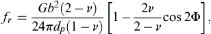
All of the mechanisms of deformation twinning are based inherently on the dissociation of lattice dislocations into twinning partials and their slip on successive {111} planes. Therefore, if these partials then move to the grain boundaries, the formation of twins will contribute to the annihilation of lattice dislocations. As a consequence, the decrease in the dislocation density between the 8th and 16th passes, as shown in Fig. 4.7, is associated with an increase in the twin boundary frequency. It is important to note that the dislocation sources are incapable of compensating for the dislocations that have disappeared by twinning because the operation of the sources is also obstructed by the newly nucleated twins. Untwinning may also occur during the deformation process due to the interaction between the dislocations and twins [16], but the present increase in the twin probability with increasing strain suggests that the twin production rate is larger than that for untwinning. The untwinning process is depicted in Fig. 4.10. The notations of dislocations in Fig. 4.10 are explained with the help of the Thompson tetrahedron presented in Fig. 4.11. The slip planes and the Burgers vectors of lattice dislocations are represented by the faces and the edges of the tetrahedron. The Burgers vectors of Schockley partial dislocations connect the vertices of the tetrahedron with the centers of the faces. For instance, the origin and the endpoint of the Burgers vector of the Schockley partial dislocation Dα in Fig. 4.10 are the points D and α in Fig. 4.11. When the leading partial αB of an initial dissociated dislocation in Fig. 4.10a meets a barrier twin boundary, it may split into a sessile stair-rod dislocation αδ and a glissile Schockley partial δB due to appropriate stresses. The Burgers vectors of stair-rod dislocations connect the centers of the faces of Thompson tetrahedron. For example, the stair-rod dislocation αδ has the Burgers vector  . The glissile Schockley partial δB slips along the twin boundary resulting in untwinning on one layer of the twin lamella. If many initial dislocations slip on successive planes and they meet the twin lamella, each dislocation causes untwinning on a layer in the lamella, which leads to a complete disappearance of a segment of the twinned region (see Fig. 4.11b). Then, further dislocations can pass freely.

Figure 4.9 The formation of twins at Lomer–Cottrell locks (a) and grain boundaries (b) by dissociation of lattice dislocations into twinning partials and their slip on successive {111} planes. The Schockley partials are denoted by “L.”

Figure 4.10 The untwinning process. The twin boundaries are indicated by “TB.” The partial dislocations are denoted as it is usual in a standard Thompson tetrahedron (see Fig. 4.11). When a dissociated dislocation meets a twin lamella, the leading partial (αB) splits into a sessile stair-rod dislocation (αδ) and a glissile Shockley partial (δB) that slips on a layer of the twin lamella resulting in untwinning on that layer (a). If dislocations on successive slip planes meet twin lamella, a complete disappearance of twin segment can occur (b).
Figure 4.11 (a) Thompson tetrahedron ABCD and (b) its two dimensional representation illustrating the possible slip planes and the Burgers vectors of dislocations in a face-centered cubic crystal. The four faces of the tetrahedron corresponding to the slip planes are denoted by a, b, c, and d while the centers of the faces are indicated as α, β, γ, and δ.
It should be noted that dynamic recovery mechanisms may also contribute to the decrease of the dislocation density in Ag between the 8th and 16th passes in a manner similar to that shown for Cu processed by more than eight passes in ECAP [22,23]. The high stresses at twin tips may assist the cross-slip of dissociated dislocations in Ag, which plays an important role in recovery whereas for Cu twinning remains marginal even when the ECAP processing is continued to extremely high strains [22,23]. However, for the case of Ag where SFE is very low, the influence of twinning on the dislocation density must also be considered as discussed earlier. It is also noted that the evolution of the defect structure is also affected by the impurity level. In UFG or nanomaterials, the segregation of alloying elements at the grain boundaries may reduce the activity of these boundaries as nucleation sites of twin lamellas since the impurities hinder the emission of twining partials.
The effect of impurity level on the evolution of defect structure in ECAP-processed Ag was investigated by a comparison of the results obtained on 4N5 and 4N purity samples [24]. The values of the mean grain size were ∼56 μm and ∼20 μm in the initial state and after one pass of ECAP, respectively, for 4N purity Ag as determined by scanning electron microscopy. TEM investigation showed that the mean grain size after four passes decreased to ∼230 nm and further ECAP deformation gave only a slight additional grain refinement. After the 8th and 16th passes the mean grain size values were ∼220 and ∼200 nm, respectively. The mean grain size in 4N5 purity Ag between the 4th and 16th passes was also ∼200 nm indicating that the two times larger impurity content in the present case did not affect significantly the minimum grain size achievable by ECAP.
The dislocation density and the twin boundary frequency were determined by X-ray line profile analysis. The dislocation density and the twin boundary frequency are plotted as a function of the number of ECAP passes for 4N purity Ag in Fig. 4.12. The evolution of the dislocation density for 4N Ag was similar to 4N5 Ag, as it increased up to eight passes and then decreased. For one pass the dislocation density was larger for 4N purity Ag (26 ± 4 × 10¹⁴ m−2) than for the more pure 4N5 sample (16 ± 2 × 10¹⁴ m−2). Gallagher [25] has shown that both the impurities and solid solution alloying reduce SFE in Ag. As for small impurity contents, the relative change of SFE has the same order of magnitude as the impurity concentration [25]; therefore in the present materials where these concentrations are not more than 10−4 the reduction of SFE due to contamination is marginal. As a consequence, the equilibrium splitting distances calculated for screw (2.51 nm) and edge dislocations (6.33 nm) in pure Ag (see Table 4.1) can be used for both 4N and 4N5 purity samples. The high degree of dislocation dissociation due to low SFE hinders dislocation annihilation, leading to a large dislocation density even after the first pass of ECAP. As this effect is similar for the two compositions, the larger dislocation density in 4N Ag after one pass can be explained solely by the stronger pinning effect of the larger concentration of impurities that hinders dislocation annihilation. Furthermore, the interaction force between dislocations and solute atoms is proportional to the square of the difference of the solute and solvent atomic sizes [26]. Therefore, the most effective pinning atoms are Pb, Bi, and Sb in the present Ag samples. The fractions of these elements in the overall impurity content are 44% and 25% for 4N and 4N5 samples, respectively; therefore the pinning effect of impurities on dislocations is much higher in 4N Ag compared to 4N5 sample than suggested by the difference in the total impurity concentrations.

Figure 4.12 The dislocation density and the twin boundary frequency as a function of number of equal-channel angular pressing (ECAP) passes for 4N purity Ag. Reprinted from Z. Hegedűs, J. Gubicza, M. Kawasaki, N.Q. Chinh, Z. Fogarassy, T.G. Langdon. The effect of impurity level on ultrafine-grained microstructures and their stability in low stacking fault energy silver, Materials Science and Engineering, A 528 (2011) 8694–8699 with permission from Elsevier.
In addition to dislocation glide, twinning also contributes to plastic deformation for both impurity levels. The twin sources are usually located at dislocation glide obstacles, such as Lomer–Cottrell locks or grain boundaries, where the local stress exceeds the critical stress needed for twin nucleation [16]. The larger dislocation density in 4N purity Ag processed by one pass increases the number of twin nucleation sites at glide obstacles, thereby leading to a higher twin boundary frequency than in 4N5 Ag.
For both impurity contents, the dislocation density increased with increasing number of passes and saturated after eight passes with a very large value of 46 ± 5 × 10¹⁴ m−2 as compared to other pure fcc metals processed by ECAP at RT [27]. This large dislocation density can be attributed to the retarded annihilation due to the high degree of dislocation dissociation. After eight passes of ECAP, the grain size is reduced to 200 nm and the majority of impurities are most probably segregated at the grain boundaries as was shown for other UFG materials [28]. As a consequence, there is a reduction in the difference between the impurity concentrations along dislocations inside the grains in 4N5 and 4N samples, which leads to similar saturation dislocation densities for the two compositions. In addition to cross-slip and climb, twinning also contributes to the annihilation of dislocations as the lattice dislocations are dissociated into twinning partials at glide obstacles and a twin forms by slipping of these partials in neighboring {111} lattice planes [17,18,20,21]. As the twin boundaries obstruct the activity of dislocation glide sources [16], the thermally activated annihilation and the dissociation due to twinning give a reduction in the dislocation density in Ag between the 8th and 16th passes. A similar decrease of the dislocation density due to dynamic recovery was observed also in Cu processed by more than eight passes in ECAP [23].
After four passes the evolution of the twin boundary frequency is different for 4N5 and 4N samples (see Fig. 4.12). In the former case, the twin boundary frequency increases monotonously up to 16 passes while for 4N specimens it decreases slightly after 8 passes. As was noted, after four passes the grain size was reduced to ∼200 nm and, due to the large number of grain boundaries, the twins are mainly nucleated at the grain boundaries as was already observed for other nanomaterials [29]. The impurities and the alloying atoms in solid solution are usually segregated at grain boundaries during SPD at RT [28]. As a consequence, the higher impurity content in 4N Ag hinders the nucleation of twins at grain boundaries. The interaction of dislocations and twins gives untwinning inside the grains [16]; therefore the reduced activity of twin sources at the grain boundaries in 4N purity Ag leads to a significant decrease in the total twin boundary frequency after 16 passes. Between the 8th and 16th passes, the lower twin formation rate in 4N purity Ag contributes to the smaller reduction of the dislocation density compared to the 4N5 purity material. It is noted that the minimum grain size achievable by ECAP at RT was also ∼200 nm for Ag with slightly higher impurity content (99.97% purity [30]). In addition, similar grain size was obtained by asymmetric rolling up to a similar strain value as in ECAP (at an equivalent strain of 6–8).
4N purity UFG Ag was also processed by high pressure torsion (HPT). Disks annealed at 741 K for 1 h were processed by HPT for 1, 10, and 20 revolutions at RT. The applied pressure and the speed of revolution were 6 GPa and 1 rpm, respectively. The mean grain size in the initial material was ∼56 μm. The microstructures of the HPT-processed disks were investigated close to the center, at the half radius, and the periphery by X-ray line profile analysis. It was found that the defect densities change only slightly along the radius of the HPT disks. Therefore, the values measured at the half radius were taken as a representative for a certain number of revolutions. The dislocation density and the twin boundary frequency reached very high values of 132 ± 13 × 1014 m−2 and 1.7 ± 0.2%, respectively, even after one revolution and they increased only slightly during further HPT processing. The maximum dislocation density and twin boundary frequency at the half radius of the HPT disks were 154 ± 16 × 1014 m−2 and 2.1 ± 0.2%, respectively, which were achieved after 20 revolutions. These defect densities are about three times larger than the saturation values for ECAP, and they can be explained by the high applied pressure of p = 6 GPa. Previous reports (e.g., Ref. [31]) have shown that in the case of ECAP the magnitude of pressure can be approximated by the flow stress (∼300 MPa for Ag [12]) that is about one order of magnitude smaller than for HPT. The high pressure applied during HPT retards vacancy migration as the migration enthalpy is the sum of the migration energy (EVM = 0.66 eV [32]) and pV where V is the volume of a vacancy (9 × 10⁻³⁰ m3 in Ag calculated as the half of the volume per atom in the lattice). For HPT-processed Ag, pV = 0.34 eV resulting in five orders of magnitude smaller diffusion coefficient than in the case of ECAP as determined by a comparison of the values of the term of  , where k is the Boltzmann constant and T is 300 K. This slower diffusion hinders the climb-controlled dislocation annihilation resulting in very large dislocation density. Previous investigations [33] on Cu having a medium SFE revealed a similar ratio between the dislocations densities reached by HPT and ECAP. However, the twinning activity in Cu was not significantly affected by the pressure. The plastic deformation in low SFE Ag occurs by both dislocation slip and twinning. The twin-faults usually form at glide obstacles such as Lomer–Cottrell locks and grain boundaries where the local stress exceeds the critical stress required for twin nucleation. The number of these nucleation sites increases if the dislocation density is higher, and this leads to a larger twin boundary frequency in the case of HPT compared with ECAP.

Figure 4.13 Transmission electron microscopy image of the microstructure in 4N Ag processed by 20 high pressure torsion revolutions [34].
TEM investigations performed at the half radius of the HPT-processed Ag disks have shown that the grain structure is similar for the HPT-processed samples irrespective of the number of revolutions [34]. Fig. 4.13 illustrates the microstructure after 20 revolutions. The mean grain size was 220 nm and is very close to the saturation values determined for the ECAP-processed specimens. This indicates that the lattice defect densities are more sensitive to the applied pressure than the grain size as was also observed for medium or high SFE fcc metals [33].
4.3. Effect of Low Stacking Fault Energy on Defect Structure in Ultrafine-Grained Alloys
In some binary systems (e.g., in Cu–Zn or Cu–Al), the alloying is accompanied by the decrease of SFE [35–37]. Therefore, the influence of low SFE on the defect structure in UFG alloys can be studied by increasing the solute atom concentration in these alloys. This effect is illustrated on nanostructured Cu, Cu–10% Zn, and Cu–30% Zn alloys having SFEs of about 62, 35, and 10 mJ/m2, respectively [38,39]. The samples were processed by HPT for five revolutions at RT. After five revolutions of HPT, the dislocation density values at the half radius of the as-processed disks are 14 ± 3, 34 ± 5, and 81 ± 7 × 10¹⁴ m−2 for 99.9% purity Cu, Cu–10% Zn, and Cu–30% Zn, respectively [38]. The corresponding crystallite size values are 60 ± 5, 60 ± 5, and 34 ± 3 nm for 99.9% purity Cu, Cu–10% Zn, and Cu–30% Zn, respectively [38]. The significant increase of dislocation density and reduction in crystallite size with increasing Zn concentration are caused partially by the effect of alloying and partially by the decrease of SFE. The smaller the SFE, the larger the degree of dislocation dissociation, and therefore the dislocation annihilation is more retarded as discussed earlier in the case of pure fcc metals. The dislocation arrangement parameter, M, obtained by X-ray line profile analysis increases with increasing Zn content in Cu [37]. This quantity characterizes the degree of screening of strain fields of dislocations: the stronger screening corresponds to smaller value of M [40]. The larger M for higher Zn concentration suggests that the arrangement of dislocations into low energy configurations is hindered by the difficult cross-slip and climb due to large solute atom content and low SFE.
It is noted that the crystallite size and the dislocation density remain unchanged within the experimental error along the radius of the disks for samples Cu and Cu–30% Zn while the crystallite size decreases and the dislocation density increases with increasing the distance from the center for specimen Cu–10% Zn [37]. The average grain sizes as obtained from TEM images are 345, 240, and 160 nm in the centers for Cu, Cu–10% Zn, and Cu–30% Zn, respectively [38]. The corresponding values in the periphery of the disks are 75, 50, and 10 nm [38]. The latter value is extremely small among the SPD-processed metals. In both the center and the periphery of the disks, the grain size decreases with increasing Zn content. It should be noted that in Cu–Zn alloys the effects of alloying and small SFE are superimposed; therefore it is difficult to separate their contributions in the increase and decrease of the dislocation density and the grain size, respectively.
While in UFG Cu twins are scarcely observed, the smaller SFE in Cu–10% Zn and Cu–30% Zn alloys results in significant twinning during HPT [38]. For Cu–10% Zn the twin boundary frequency values are 0.16, 0.82, and 1.36% at the center, half radius, and periphery of the disk, respectively [38]. The corresponding values for Cu–30% Zn are 1.82, 2.88, and 3.73%, respectively [38]. In UFG or nanostructured Cu–Al alloys processed by SPD, the increment of twin density with increasing Al content was also observed, which can be also explained by the decrease of SFE [37,41]. For Cu–5 at.% Al, Cu–8 at.% Al, and Cu–16 at.% Al alloys, the values of SFE are 28, 17, and 6 mJ/m2, respectively [37]. The twin boundary frequency achieved by SPD for some nanostructured low SFE metals and alloys are listed in Table 4.2. In most cases, the twin boundary frequency is determined by X-ray line profile analysis. When X-ray data are not available, the percentage twin boundary frequency (β) is estimated from the mean spacing (dtwin) between twin boundaries in TEM images as:
![]() (4.15)
(4.15)
where d111 is the distance between the neighboring {111} planes. The twin boundary frequency data in Table 4.2 are plotted as a function of SFE in Fig. 4.14. It is revealed that the large twin boundary frequency is basically caused by the low SFE. At the same time, for same or similar SFE values, the smaller grain size is accompanied by larger twin boundary frequency. It is noted that, in medium or high SFE metals (e.g., in Cu or Al) twinning is also observed if the grain size is very small (about 20 nm) [42,43]. The effect of grain size on twinning activity during deformation is presented in Chapter 7.
Table 4.2
The maximum values of the twin boundary frequency achieved by severe plastic deformation for some nanostructured low SFE metals and alloys
| Material | Processing method | SFE (mJ/m2) | Grain size (nm) | Twin boundary frequency (%) | References |
| Au | 4 ECAP at RT | 38 [2,3] | 460 | 0.3 (XRD) | [44] |
| Ag | 16 ECAP at RT | 19 [2,3] | 200 | 1.5 (XRD) | [12] |
| Ag | 20 HPT at RT | 19 [2,3] | 220 | 2.1 (XRD) | [34] |
| Cu–10% Zn | 5 HPT at RT, disk center | 35 [22] | 240 | 0.16 (XRD) | [38] |
| Cu–10% Zn | 5 HPT at RT, disk periphery | 35 [22] | 50 | 1.36 (XRD) | [38] |
| Cu–30% Zn | 5 HPT at RT, disk center | 10 [22] | 160 | 1.82 (XRD) | [38] |
| Cu–30% Zn | 5 HPT at RT, disk periphery | 10 [22] | 10 | 3.73 (XRD) | [38] |
| Cu–5% Al | 4 ECAP at RT | 28 [35] | 107 | ∼1 (TEM) | [37] |
| Cu–8% Al | 4 ECAP at RT | 17 [35] | 82 | ∼2 (TEM) | [37] |
| Cu–16% Al | 2 ECAP at RT | 6 [35] | 50 | ∼2 (TEM) | [37] |


Figure 4.14 The twin boundary frequency as a function of stacking fault energy (SFE). The grain size is also given at some data points. The data are taken from Table 4.2.
It is noted that very high twin-fault probability was also observed in nanostructured low SFE materials processed by bottom-up processing methods. For instance, in Ag thin films deposited by magnetron sputtering the twin spacing depended on the crystallographic orientation [45]. High density of twin-faults oriented normal to the film growth direction with an average spacing of ∼9 nm is observed in the columnar grains of the (111) oriented films. The thickness of the columns was ∼120 nm. This twin boundary spacing corresponds to a twin-fault probability of 2.6%. Twins are also observed in the (110) oriented films with a much lower twin density (i.e., with much higher twin spacing of ∼42 nm), and the twin boundaries on (111) planes are oriented ∼55 degrees from the growth direction. The latter twin boundary spacing corresponds to a twin-fault probability of 0.6%. It can be concluded that similar twin-fault probability values were obtained for UFG Ag processed by either top-down or bottom-up procedures.
4.4. Grain-Refinement Mechanisms in Low Stacking Fault Energy Alloys
In the case of materials having medium or high SFE, dislocation activities play a major role in the grain refinement during SPD procedures. During SPD processes, dislocations are formed, interact with each other, and rearrange into cell and subgrain boundaries. With increasing strain in SPD, the misorientation between neighboring subgrains increases and they become high-angle grain boundaries thereby resulting in a refinement of the initial coarse grains. Simultaneously, new subgrain boundaries are formed by dislocation accumulation in the refined grains that yields further grain refinement. For materials with low SFEs, it is expected that SFs and twin boundaries formed during deformation play a significant role in grain refinement. The strong effect of SFE on the grain-refinement mechanisms and the minimum achievable grain size is demonstrated on Cu–30% Zn alloy having extremely low SFE of about 10 mJ/m2, which was subjected to five revolutions by HPT at RT [46]. As the imposed strain is linearly proportional to the distance from the center in HPT-processed disks, the different stages of microstructural evolution were studied by selecting various positions on the disk processed by five revolutions.
The steps of grain refinement as observed in TEM images are depicted in the schematic drawing of Fig. 4.15 [46]. In the first step, the initial equiaxed ultrafine grains with grain sizes of hundreds of nanometers are divided into elongated regions having widths of about 10 nm through the formation of a high density of SFs and twins. Most of the SFs and twins are formed through partial dislocation emission from grain boundaries and some of them terminate in grain interiors [46]. A few twins may form through a dissociation of lattice dislocation into two partials as both ends terminate within a grain.

Figure 4.15 Schematic illustration of the grain-refinement mechanism for the Cu–30 wt.% Zn alloy processed by high pressure torsion. HAGB, high-angle grain boundary; SF, stacking fault; TB, twin boundaries. After Y.B. Wang, X.Z. Liao, Y.H. Zhao, E.J. Lavernia, S.P. Ringer, Z. Horita, T.G. Langdon, Y.T. Zhu. The role of stacking faults and twin boundaries in grain refinement of a Cu–Zn alloy processed by high-pressure torsion, Materials Science and Engineering, A 527 (2010) 4959–4966 with permission from Elsevier.
In step 2 (see Fig. 4.15), a high density of dislocations accumulates at SFs and twin boundaries; therefore the original atomically flat coherent SFs and twin boundaries evolve into curved incoherent high-angle grain boundaries (step 3). The HRTEM image in Fig. 4.16 shows dislocations blocked at a twin boundary resulting in an 8-degree deviation from the ideal misorientation between the twins [46]. In step 4, secondary SFs and twins were emitted from these boundaries as illustrated in Fig. 4.15 [46]. Finally, in step 5 the emission of secondary SFs and twins further refines the grains and transforms the elongated grains into equiaxed grains having a grain size of 10 nm. The experimental observations presented earlier suggest that both dislocations and twin boundaries participate in the grain refinement during SPD of low SFE materials. First, twin boundaries divide the initial grains into smaller parts, and then these twin boundaries will be transformed into incoherent grain boundaries by accumulation of gliding dislocations. The final grain size of 10 nm is extremely low among the HPT-processed metals that can also be attributed to the effect of high alloying element concentration in addition to the low SFE as the solute atoms hinder the recovery and recrystallization of the nanostructure. It is worth to note that an amorphous structure was also formed at the incoherent boundaries of the final nanocrystalline grains [46].

Figure 4.16 A high-resolution transmission electron microscopy image of a bent twin boundary (TB) in high pressure torsion-processed Cu–30% Zn alloy showing a high density of dislocations, which are indicated using white and black “T,” accumulated at the TB. Two white solid lines were drawn parallel to {111} at each side of the TB, respectively, and one dash white line was also drawn parallel to (111)M to indicate the misorientation between the {111} planes across the TB. Reprinted from Y.B. Wang, X.Z. Liao, Y.H. Zhao, E.J. Lavernia, S.P. Ringer, Z. Horita, T.G. Langdon, Y.T. Zhu. The role of stacking faults and twin boundaries in grain refinement of a Cu–Zn alloy processed by high-pressure torsion, Materials Science and Engineering, A 527 (2010) 4959–4966 with permission from Elsevier.
Similar effect of low SFE on grain-refinement mechanisms can be observed in Cu–Al alloys processed by ECAP at RT [26]. With increasing the Al content in Cu–Al alloys, the SFE decreases [37]. For Cu–5 at.% Al alloy, although the grain refinement is dominated by the dislocation activity, twinning also has a contribution to the decrease of grain size. The increase of Al concentration yields a gradual transformation of the ECAP-induced grain-refinement mechanism from dislocation subdivision to twin fragmentation [37]. Similarly to HPT-processed Cu–30% Zn alloy, primary and secondary twin boundaries are formed after the second ECAP pass and they facilitate the grain refinement. The grain size values after four passes for Cu–5 at.% Al and Cu–8 at.% Al alloys are 107 and 82 nm, respectively, while the grain size for Cu–16 at.% Al after two passes is 50 nm [37]. These values are very low among the ECAP-processed materials that can be attributed to the combined effect of alloying and low SFE as discussed earlier. It is worth to note that the HPT-processed Cu–30% Zn alloy has much smaller grain size (10 nm) than Cu–16 at.% Al alloy after two passes of ECAP despite their very similar SFE (about 10 mJ/m2). This difference may be caused by the larger solute atom concentration in Cu–30% Zn alloy. The effectiveness of twinning mechanism in grain refinement is also manifested in the much higher fraction of high-angle grain boundaries in Cu–8 at.% Al alloy (62%) compared to Cu–5 at.% Al alloy (49%) [37].
..................Content has been hidden....................
You can't read the all page of ebook, please click here login for view all page.