
Chapter 9
Effect of Lattice Imperfections on Electrical Resistivity of Nanomaterials
Abstract
In this chapter the influence of lattice defects (vacancies, vacancy clusters, dislocations, planar faults, and grain boundaries) on the electrical resistivity of ultrafine-grained (UFG) and nanocrystalline materials is overviewed. First, the residual resistivities caused by different defects are compared with the intrinsic resistivity at different temperatures. It turned out that the resistivities of vacancies, dislocations, and twin faults are much smaller than that for high-angle grain boundaries (HAGBs), solute atoms, and the intrinsic resistivity at room temperature. For pure metals and equilibrium solid solutions, nanocrystallization by severe plastic deformation (SPD) methods yields only a few percentage increase in resistivity while the strength is improved considerably, thereby improving the strength-to-resistivity ratio. The addition of solute atoms to metallic matrices leads to an increment in both strength and resistivity in SPD-processed UFG materials; however, the strength-to-resistivity ratio is only slightly changed. The best combination of high strength and good conductivity in alloys is obtained if the strengthening is achieved by grain boundaries and nanosized secondary phase particles while the grain interiors are purified from solute elements. This microstructure can be processed by a sequential application of SPD and annealing. In pure metallic materials an improvement in strength-to-resistivity ratio can be achieved if the majority of HAGBs are substituted by coherent twin faults as the latter interfaces have very low specific electrical resistivity. In electrodeposited and sputtered films, nanoscale growth twin lamellae in UFG grains give a strong increase in strength while the conductivity is only slightly smaller than that for a coarse-grained defect-free material.
Keywords
Conductivity; Dislocation; Electrical resistivity; Grain boundary; Stacking fault; Twin fault; Vacancy
9.1. Contribution of Lattice Defects to Electrical Resistivity
Crystal lattice has a resistivity against electric current since the conducting electrons are scattered by phonons. This phenomenon is referred to as intrinsic resistivity of crystalline materials (hereafter denoted as ri). The intrinsic resistivity is the electrical resistivity of a defect-free and chemically pure material. With decreasing temperature (T) lattice vibrations diminish; therefore, intrinsic resistivity strongly decreases. For metallic materials the resistivity at high temperatures (e.g., for Cu between 100 K and the melting point) is a linear function of T [1,2]. As the temperature is reduced, the temperature dependence of resistivity follows. At lower temperatures the resistivity varies with ∼T5 (if scattering by phonons is the main contribution), and the resistivity becomes constant at 10–20 K. This residual resistivity is caused by the lattice defects and the impurities, i.e., it is not related to the intrinsic resistivity. As an example, Fig. 9.1 illustrates the temperature dependence of resistivity of Cu in double logarithmic scale.
Lattice defects such as vacancies, interstitials, dislocations, stacking faults, grain boundaries, and solute atoms have considerable contributions to electrical resistivity. The intrinsic resistivity of a crystalline material and the contributions of different lattice defects (rl) are summed up in the total electrical resistivity (r) as discussed in Chapter 2 (Matthiessen's rule):

Figure 9.1 The electrical resistivity of coarse-grained pure Cu as a function of temperature between 1 and 1356 K (the melting point of Cu) [1].
![]() (9.1)
(9.1)
where T is the temperature and index l stands for the different lattice defects (including impurities and alloying elements). The contributions of lattice defects are practically independent of the temperature but increase with increasing concentrations or densities of defects. For vacancies, dislocations, stacking faults, twin faults (twin boundaries), and high-angle grain boundaries (HAGBs) the resistivity contributions can be approximated as:
![]() (9.2)
(9.2)
![]() (9.3)
(9.3)
![]() (9.4)
(9.4)
![]() (9.5)
(9.5)
![]() (9.6)
(9.6)
respectively, where ηv, ηd, ηsf, ηTB, and ηHAGB are the resistivity increments for unit vacancy concentration, dislocation density (given in m−2), stacking fault density (ρsf given in m−1), twin fault density (ρTB given in m−1), and HAGB density (ρHAGB given in m−1). The quantity ρsf gives the area of stacking faults in a unit volume of material. ρTB and ρHAGB are defined similarly. It is noted that the planar fault or grain boundary density can be given as the reciprocal of the fault or boundary spacing, respectively. Table 9.1 lists the values of the specific resistivities ηv, ηd, ηsf, ηTB, and ηHAGB for Cu. It should be noted that the specific resistivity of interstitials is about three times larger than that for vacancies. In addition, the electrical resistivity of a divacancy is about 20% less than the electrical resistivity of two separated vacancies [3]. It was shown that the specific resistivity of a vacancy in Cu is approximately the same in the temperature range between 4 K and the melting point [4]. It should also be noted that the resistivity of HAGBs depends on the structure of HAGBs. For instance, in Cu the value of ηHAGB decreased from 5.5 × 10⁻¹⁶ to 2 × 10⁻¹⁶ Ωm2 due to grain boundary relaxation during annealing [4].
Table 9.1
Specific electrical resistivities for vacancies, dislocations, stacking faults, twin faults, and general high-angle grain boundaries (HAGBs) in Cu
| Metal | Vacancy, ηv (Ωm) | Dislocation, ηd (Ωm3) | Stacking fault, ηsf (Ωm2) | Twin fault, ηTB (Ωm2) | Grain boundary, ηHAGB (Ωm2) |
| Cu | 1.9 × 10⁻⁶ | 1.3 × 10⁻²⁵ | 3.4 × 10⁻¹⁷ | 1.7 × 10⁻¹⁷ | 3.4 × 10⁻¹⁶ |

Instead of ρTB the amount of twin faults is often characterized by the quantity called as twin fault probability (β). In face-centered cubic (fcc) structures β is defined as the fraction of faulted planes among {111} crystallographic planes. If only one {111}-type plane is populated with twin faults in each grain, the value of ρTB is equivalent to the reciprocal of twin fault spacing, and β can be expressed by ρTB as:
![]() (9.7)
(9.7)
where d111 is the spacing between the neighboring {111} planes and β is given in percentage. Inserting Eq. (9.7) into Eq. (9.5), the resistivity caused by twin faults can be related to twin fault probability as:
![]() (9.8)
(9.8)
Similar considerations hold for stacking faults as well. For a cubic grain shape the resistivity of HAGBs can be expressed with the grain size (d) as:
![]() (9.9)
(9.9)
Impurities and alloying elements, except for silver, increase the electrical resistivity of Cu. For a given concentration, the effect of solute atoms on the resistivity of Cu increases in the following order: Pb, Zn, Ni, Al, Sn, Sb, Mn, Cr, Si, Fe, and P. For instance, 1 at.% Zn, Ni, Al, or Sn causes ∼0.3, 1.2, 1.5, or 3 × 10⁻⁸ Ωm increment in resistivity of Cu, respectively [11–13]. It is noted that with increasing oxygen content in Cu, the resistivity first decreases, but above ∼200 ppm oxygen the resistivity starts to increase similar to effect of other solute elements. For a given alloying element concentration, the resistivity of solid solution state is higher than that for a precipitation microstructure. Simply saying, the purer the matrix, the lower the resistivity.
The electrical resistivities caused by different lattice defects and solute atoms in Cu are compared with the intrinsic resistivity in Fig. 9.2. The plotted resistivity ranges correspond to lattice defect densities characteristic to nanostructured Cu materials. It can be seen that the resistivities of vacancies, dislocations, and twin faults are much smaller than the effects of HAGBs, solute atoms, and the intrinsic resistivity at room temperature (RT). Therefore, if the lattice defect densities are intended to be determined by resistivity measurements, the experiments are usually carried out at very low temperatures where the intrinsic resistivity is relatively small (e.g., at liquid nitrogen or helium temperature with the value of 77 or 4 K, respectively) [8].

In nanomaterials sintered from powders, the porosity also increases resistivity. The total resistivity can be expressed as the product of the resistivity of the porosity-free matrix (rm) and a factor describing the effect of pores (f(Vp)) [14–16]:
![]() (9.10)
(9.10)
where Vp is the volume fraction of pores. For Vp < 0.5, the porosity factor, f(Vp), can be expressed as (Wiedemann–Franz–Lorenz equation) [15]:
 (9.11)
It should be noted, however, that the Schroeder formula elaborated for the description of the effect of precipitates on resistivity [16] can also be adopted for the calculation of the porosity factor [14]:
![]() (9.12)
(9.12)
Fig. 9.3 shows the variation of the porosity factor as a function of volume fraction of pores according to Eqs. (9.11) and (9.12).
The electrical conductivity of metallic materials is often expressed in terms of percentage IACS. IACS is the abbreviation of International Annealed Copper Standard, and 100% IACS is equivalent to the conductivity of a commercially pure annealed copper. The standard was established in 1913 by the International Electrotechnical Commission. 100% IACS at 20 °C corresponds to conductivity of ∼5.8 × 10⁷ S/m or resistivity of ∼1.72 × 10⁻⁸ Ωm. The application of IACS is especially useful when change of conductivity of copper samples is investigated during annealing since the variation of IACS reflects the influence of lattice defects, chemical, and phase compositions on conductivity (i.e., the change of temperature independent residual resistivity). For instance, 20% IACS at a given temperature is equivalent to 20% of the conductivity of an annealed pure Cu at the same temperature. It is noted that conductivities higher than 100% IACS are often measured nowadays for Cu since the improved processing techniques may produce higher purity Cu with a better conductivity than that obtained in 1913.

9.2. Change of Resistivity in Nanomaterials Processed by Severe Plastic Deformation
The electrical resistivity increment caused by monovacancies, vacancy clusters, and dislocations was determined in high purity ultrafine-grained (UFG) Ni and Cu [8]. The resistivity contribution of single and double vacancies in 99.998% purity Ni processed by two turns of high-pressure torsion (HPT) at RT was about 3 × 10⁻¹⁰ Ωm, which was caused by a vacancy concentration of ∼10−4. This value was measured at the periphery of the HPT-processed disk where the strain was the largest. The resistivity increment caused by vacancy agglomerates, dislocations, and HAGBs was ∼17 × 10−10 Ωm. It was found that the resistivity increment caused by the lattice defects formed in Ni during HPT saturated at a shear strain of ∼20, which can be achieved already at the periphery of a disk deformed by one-third turn of HPT. After one turn of HPT, both resistivity and strength in Ni change only slightly with increasing either the distance from the disk center or the number of turns [17]. It is worth to note that the contribution of lattice defects to resistivity in HPT-processed Ni (∼20 × 10−10 Ωm) is two orders of magnitude larger than the intrinsic resistivity measured at 4 K. At the same time, at RT the resistivity of lattice defects is only ∼10% of the intrinsic electrical resistivity of Ni. In UFG copper processed by five passes of equal-channel angular pressing (ECAP) at RT the lattice defects formed during severe plastic deformation (SPD) yielded a resistivity increment of ∼4 × 10⁻¹⁰ Ωm, irrespective of the applied ECAP route (A, BC, and C, as defined in Chapter 3) [18]. The change of resistivity for ECAP-processed Cu is much smaller than that in Ni deformed by HPT, which can be explained by the much lower shear strain applied in the former method (∼5). The contribution of lattice defects to resistivity of ECAP-processed pure Cu at RT is only ∼2%. Similar results were obtained for 99.96% purity UFG copper produced by 16 passes of ECAP via route BC at RT [19]. Although, the grain size was refined from 6 μm to 500 nm when the annealed Cu sample was processed by 16 ECAP passes, the conductivity changed only from 97% IACS to 95% IACS, i.e., the contribution of lattice defects (including vacancies, dislocations, and grain boundaries) to resistivity is only ∼2%. In Cu–3 wt.% Ag alloy 12 passes of ECAP at 343 K yielded reduction of conductivity from 94% to 88% IACS [20]. Generally, it can be concluded that in pure metals and equilibrium solid solutions, SPD results only in a slight increase of resistivity owing to the increase of amount of lattice defects. At the same time, the lattice defects result in a strong increase of mechanical strength. For instance, the yield strength in pure copper increased from ∼100 to ∼350 MPa owing to 16 ECAP passes [19]. Therefore, SPD methods usually significantly improve the strength-to-resistivity ratio. In the case of Cu processed by 16 passes of ECAP, the strength-to-resistivity ratio increased from 0.56 × 10¹⁰ to 1.9 × 10¹⁰ MPa/Ωm. At the same, for low carbon steel four passes of constrained groove pressing (CGP) led to only a 20% increment in strength-to-resistivity ratio [21]. In the CGP process the grain size of the steel was refined from 30 μm to 231 nm. Table 9.2 summarizes the grain size, the mechanical strength, the conductivity in IACS, the electrical resistivity, and the strength-to-resistivity ratio for different UFG and nanocrystalline materials. In the present case, the mechanical strength is characterized by the yield strength or the strength calculated as one-third of the hardness, depending on the availability of these data. It should be noted that the stress determined as one-third of hardness gives the flow stress corresponding to 8% plastic strain since hardness measurement itself yields an additional plastic deformation. For materials exhibiting strong strain hardening after the onset of yielding, one-third of hardness may be considerably larger than the yield strength. At the same time, for SPD-processed samples the strain hardening is usually moderate; therefore, there is only a slight difference between one-third of hardness and yield strength.
The addition of alloying elements to coarse-grained metallic materials increases both strength and resistivity; however, the former effect is usually stronger, thereby improving the strength-to-resistivity ratio. For instance, in coarse-grained Cu–0.18% Zr alloy the strength-to-resistivity ratio is 25%–55% higher than in pure Cu [22]. The smaller and larger increments are related to precipitation microstructure and solid solution, respectively. In SPD-processed UFG copper materials, the addition of small amount of solute atoms yields similar relative increase in both strength and electrical resistivity, resulting in practically unchanged strength-to-resistivity ratio, as shown in Table 9.2. At the same time, secondary phase particles (e.g., alumina) in ECAP-processed Cu matrix can improve the strength-to-resistivity ratio by about 50% since the strength increased considerably without significant reduction of conductivity [23]. It should be noted, however, that the conductivity of Cu–alumina composites processed by powder metallurgy techniques are very poor (see Table 9.2), most probably due to the remaining porosity [14,24,25]. The best behavior was observed for Cu–3wt.% Ag alloy processed by eight passes of ECAP at 343 K, as for this material the strength-to-resistivity ratio is about 50% higher than that for pure ECAP-processed Cu with similar grain size [20]. In this alloy, silver addition increased the strength considerably, while the conductivity was only slightly reduced.
Table 9.2
Grain size, mechanical strength, conductivity in IACS, resistivity, and strength-to-resistivity ratio measured at RT for different UFG and nanocrystalline materials
| Material and processing method | Grain size (nm) | Strength (MPa) | Conductivity in IACS (%) | Resistivity (10−8 Ωm) | Strength-to-resistivity ratio (1010 MPa/Ωm) | References |
| 99.96% purity Cu, 16 ECAP at RT | 500 | 350 | 95 | 1.8 | 1.9 | [19] |
| 99.999% purity Cu film, magnetron sputtering, twin spacing: 7 nm | 70 | 930∗ | 74 | 2.3 | 4.0 | [10,26] |
| 99.999% purity Cu film, magnetron sputtering, twin spacing: 16 nm | 146 | 700∗ | 100 | 1.7 | 4.1 | [10,26] |
| 99.998% purity Cu, pulsed electrodeposition, twin spacing: 15 nm | 400 | 900 | 97 | 1.75 | 5.1 | [27] |
| Cu, SPS + CD | 220 | 590 | 78 | 2.2 | 2.7 | [28] |
| Cu–0.18 wt.% Zr with Cu5Zr precipitates, 15 HPT at RT | 200 | 530∗ | 59 | 2.9 | 1.8 | [22] |
| Cu–0.18 wt.% Zr solid solution, 15 HPT at RT | 200 | 570∗ | 51 | 3.4 | 1.7 | [22] |
| Cu–0.18 wt.% Zr with Cu5Zr precipitates, 15 HPT at RT + annealing for 1 h at 723 K | – | 570∗ | 75 | 2.3 | 2.5 | [22] |
| Cu–0.18 wt.% Zr solid solution, 15 HPT at RT + annealing for 1 h at 723 K | – | 600∗ | 57 | 3.0 | 2.0 | [22] |
| Cu–3 wt.% Ag, 8 ECAP at 343 K | 350 | 617 | 88 | 1.9 | 3.2 | [20] |
| Cu–1.1 wt.% Al2O3, cold spray | 37 | 700∗ | 31 | 5.5 | 1.3 | [14] |
| Cu–1.1 wt.% Al2O3, cold spray + annealing at 1223 K | 55 | 670∗ | 47 | 3.7 | 1.8 | [14] |
| Cu–1vol.% Al2O3, ball milling + HIP | 170 | 460 | 50 | 3.4 | 1.4 | [24] |
| Cu–5vol.% Al2O3, ball milling + HIP | 170 | 620 | 44 | 3.9 | 1.6 | [24] |
| Cu–4 wt.% Al2O3, ball milling + compaction by hot-pressing | – | 600∗ | 47 | 3.7 | 1.6 | [25] |
| Cu–0.5 wt.% Al2O3, 4 ECAP at RT | 370 | 525 | 86 | 2.0 | 2.6 | [23] |
| Table Continued | ||||||

| Material and processing method | Grain size (nm) | Strength (MPa) | Conductivity in IACS (%) | Resistivity (10−8 Ωm) | Strength-to-resistivity ratio (1010 MPa/Ωm) | References |
| Cu–1.1 wt.% Al2O3, 4 ECAP at RT | 350 | 560 | 82 | 2.1 | 2.7 | [23] |
| Cu–0.3 wt.% Mg–0.05 wt.% Ce, 8 ECAP at RT | 600 | 520 | 72 | 2.4 | 2.2 | [29] |
| Cu–0.3 wt.% Mg–0.05 wt.% Ce, 8 ECAP at RT + annealing for 2 h at 573 K | – | 510 | 75 | 2.3 | 2.2 | [29] |
| Cu–0.2 wt.% Mg, 4 ECAP + CR + CD at RT | 100–200 | 567 | 82 | 2.1 | 2.7 | [30] |
| Cu–0.2 wt.% Mg, 4 ECAP + CR + CD at RT + annealing for 2 h at 573 K | – | 426 | 87 | 2.0 | 2.1 | [30] |
| Cu–0.4 wt.% Mg, 4 ECAP + CR + CD at RT | 100–200 | 597 | 72 | 2.4 | 2.5 | [30] |
| Cu–0.4 wt.% Mg, 4 ECAP + CR + CD at RT + annealing for 2 h at 573 K | – | 488 | 80 | 2.1 | 2.3 | [30] |
| Cu–0.75 wt.% Cr, Q + 5 HPT at RT | 209 | 580∗ | 34 | 5.0 | 1.2 | [31] |
| Cu–0.75 wt.% Cr, Q + 5 HPT at RT + annealing for 1 h at 523 K | 245 | 610∗ | 35 | 4.9 | 1.2 | [31] |
| Cu–0.75 wt.% Cr, SC + 5 HPT at RT | – | 537∗ | 61 | 2.8 | 1.9 | [31] |
| Cu–0.75 wt.% Cr, SC + 5 HPT at RT + annealing for 1 h at 523 K | – | 478∗ | 72 | 2.4 | 2.0 | [31] |
| Cu–9.85 wt.% Cr, Q + 5 HPT at RT | 143 | 713∗ | 29 | 5.9 | 1.2 | [31] |
| Cu–9.85 wt.% Cr, Q + 5 HPT at RT + annealing for 1 h at 773 K | 229 | 584∗ | 67 | 2.6 | 2.2 | [31] |
| Cu–9.85 wt.% Cr, SC + 5 HPT at RT | – | 702∗ | 54 | 3.2 | 2.2 | [31] |
| Cu–9.85 wt.% Cr, SC + 5 HPT at RT + annealing for 1 h at 773 K | – | 631∗ | 76 | 2.3 | 2.7 | [31] |
| Cu–27 wt.% Cr, as-cast + 5 HPT at RT | 40 | 900∗ | 20 | 8.6 | 1.1 | [31] |
| Cu–27wt.% Cr, as-cast + 5 HPT at RT + annealing for 1 h at 773 K | 96 | 879∗ | 42 | 4.1 | 2.1 | [31] |
| Table Continued | ||||||

| Material and processing method | Grain size (nm) | Strength (MPa) | Conductivity in IACS (%) | Resistivity (10−8 Ωm) | Strength-to-resistivity ratio (1010 MPa/Ωm) | References |
| Cu–0.9 wt.% Hf, Q + 5 HPT at RT | 155 | 660∗ | 41 | 4.2 | 1.6 | [32] |
| Cu–0.9 wt.% Hf, Q + 5 HPT at RT + annealing for 1 h at 723 K | 189 | 800∗ | 71 | 2.4 | 3.3 | [32] |
| Cu–0.9 wt.% Hf, SC + 5 HPT at RT | – | 660∗ | 50 | 3.4 | 1.9 | [32] |
| Cu–0.9 wt.% Hf, SC + 5 HPT at RT + annealing for 1 h at 723 K | – | 600∗ | 80 | 2.1 | 2.9 | [32] |
| Cu–0.7 wt.% Cr–0.9 wt.% Hf, Q + 5 HPT at RT | 108 | 800∗ | 23 | 7.4 | 1.1 | [32] |
| Cu–0.7 wt.% Cr–0.9 wt.% Hf, Q + 5 HPT at RT + annealing for 1 h at 773 K | 131 | 933∗ | 61 | 2.8 | 3.3 | [32] |
| Cu–0.7 wt.% Cr–0.9 wt.% Hf, SC + 5 HPT at RT | – | 673∗ | 46 | 3.7 | 1.8 | [32] |
| Cu–0.7 wt.% Cr–0.9 wt.% Hf, SC + 5 HPT at RT + annealing for 1 h at 773 K | – | 770∗ | 67 | 2.6 | 3.0 | [32] |
| 99.5 wt.% Al, 10 HPT at RT | 810 | 200∗ | 57 | 3.0 | 0.7 | [33] |
| Al–0.3 wt.% Si–0.4 wt.% Fe (AA 1050), 4 HE at RT | 449 | 167∗ | 60 | 2.8 | 0.6 | [34] |
| Al–0.3 wt.% Si–0.4 wt.% Fe (AA 1050), 4 ECAP at RT | 539 | 163∗ | 60 | 2.8 | 0.6 | [34] |
| Al–0.3 wt.% Si–0.4 wt.% Fe (AA 1050), 2 ECAP + 4 HE at RT | 454 | 167∗ | 59 | 2.9 | 0.6 | [34] |
| Al–4.6 wt.% Mg–0.9 wt.% Mn–0.1 wt.% Si–0.1 wt.% Fe (AA 5483), 4 HE at RT | 199 | 510∗ | 26 | 6.6 | 0.8 | [34] |
| Al–4.6 wt.% Mg–0.9 wt.% Mn–0.1 wt.% Si–0.1 wt.% Fe (AA 5483), 2 ECAP at RT | 215 | 437∗ | 26 | 6.6 | 0.7 | [34] |
| Al–4.6 wt.% Mg–0.9 wt.% Mn–0.1 wt.% Si–0.1 wt.% Fe (AA 5483), 2 ECAP + 4 HE at RT | 185 | 493∗ | 26 | 6.6 | 0.8 | [34] |
| Al–0.8 wt.% Mg–0.8 wt.% Si–0.1 wt.% Fe alloy (Al 6201), 20 HPT at RT | 130 | 448 | 48 | 3.6 | 1.2 | [35] |
| Table Continued | ||||||

| Material and processing method | Grain size (nm) | Strength (MPa) | Conductivity in IACS (%) | Resistivity (10−8 Ωm) | Strength-to-resistivity ratio (1010 MPa/Ωm) | References |
| Al–0.8 wt.% Mg–0.8 wt.% Si–0.1 wt.% Fe alloy (Al 6201), 20 HPT at 403 K | 280 | 380 | 56 | 3.1 | 1.2 | [35] |
| Al–0.8 wt.% Mg–0.8 wt.% Si–0.1 wt.% Fe alloy (Al 6201), 20 HPT at 453 K | 440 | 326 | 58 | 2.9 | 1.1 | [35] |
| Al–0.8 wt.% Mg–0.8 wt.% Si–0.1 wt.% Fe alloy (Al 6201), 20 HPT at 503 K | 960 | 218 | 59 | 2.9 | 0.8 | [35] |
| Al–0.6 wt.% Mg–0.5 wt.% Si–0.1 wt.% Fe alloy (Al 6101), 20 HPT at RT | 180 | 570∗ | 47 | 3.7 | 1.5 | [36] |
| Al–0.6 wt.% Mg–0.5 wt.% Si–0.1 wt.% Fe alloy (Al 6101), 20 HPT at 373 K | 240 | 440∗ | 52 | 3.3 | 1.3 | [36] |
| Al–0.6 wt.% Mg–0.5 wt.% Si–0.1 wt.% Fe alloy (Al 6101), 20 HPT at 443 K | 430 | 240∗ | 59 | 2.9 | 0.8 | [36] |
| Al–5.4 wt.% Ce–3.1 wt.% La, 20 HPT at RT | 136 | 475 | 40 | 4.3 | 1.1 | [37] |
| Al–5.4 wt.% Ce–3.1 wt.% La, 20 HPT at RT + annealing for 1 h at 553 K | 203 | 495 | 45 | 3.9 | 1.3 | [37] |
| Al–5.4 wt.% Ce–3.1 wt.% La, 20 HPT at RT + annealing for 1 h at 673 K | 385 | 255 | 52 | 3.3 | 0.8 | [37] |
| Ti (50% α + 50% ω), 10 HPT at 100 K | 54 | 1300∗ | 2.1 | 80 | 0.16 | [38] |
| Ti (20% α + 80% ω), 10 HPT at RT | 118 | 1200∗ | 1.9 | 90 | 0.13 | [38] |
| Fe–0.2 wt.% Mn (low carbon steel), 4 CGP at RT | 231 | 400 | 1.7 | 100 | 0.04 | [21] |

It is worth to note that SPD processing may yield not only the increase of the amount of lattice defects but also phase transformation, which influences the electrical resistivity. For instance, HPT under 6 GPa pressure can result in a transformation from hexagonal close-packed (hcp) α structure to hexagonal ω phase [38]. The electrical resistivity of the latter phase at RT is about two times larger (∼1.0 × 10⁻⁶ Ωm) than that for α-Ti (∼0.5 × 10⁻⁶ Ωm). The ω phase transforms back to hcp structure after annealing the HPT-processed samples at ∼400 K, which results in a decrease of resistivity. It is noted that the strength-to-resistivity ratio is very small for the HPT-processed two-phase α/ω titanium materials (0.13–0.16 × 10¹⁰ MPa/Ωm) due to the high fraction of ω phase, as compared to other SPD-processed pure materials (see Table 9.2). In two-phase alloys, SPD often causes dissolution of equilibrium phases as the solubility limit of alloying elements in the matrix can be increased due to their preferred storage at defects, such as dislocations and grain boundaries. This dissolution usually increases the electrical resistivity due to the scattering of conductive electrons on solute atoms. This phenomenon was observed in Cu–0.18 wt.% Zr alloys during processing via 15 turns of HPT at RT [22]. HPT deformation yielded a partial dissolution of secondary phase particles of Cu5Zr into Cu matrix besides the formation of lattice defects. Both processes have contributions to the increase of resistivity from ∼2.3 × 10⁻⁸ to ∼2.9 × 10⁻⁸ Ωm during HPT. Since this SPD processing resulted in a higher change of yield strength (from ∼200 to ∼530 MPa) than the increment in resistivity, HPT led to an increase in strength-to-resistivity ratio from 0.9 × 10¹⁰ to 1.8 × 10¹⁰ MPa/Ωm. When the initial state was a solid solution with the same composition, both the strength and resistivity changes caused by HPT were higher; however, the strength-to-resistivity ratio remained practically the same [22]. This ratio for Cu–0.18 wt.% Zr alloy can be improved by an additional annealing after HPT as it will be discussed in Section 9.4. In Al alloys SPD processing by hydrostatic extrusion, ECAP, and their combination yielded a significant improvement in strength while the resistivity increased only by ∼2%, similar to copper alloys [34]. Therefore, the strength-to-resistivity ratio was improved with a factor of about two for both low and high solute concentrations (AA 1050 and AA 5483 alloys). It is also worth to note that for alloys with high solute contents, the degree of disorder also influences strongly the electrical resistivity. For instance, SPD processing of Cu–40 at.% Pd alloy may yield transition from ordered B2 structure to disordered fcc A1 phase, which increases the resistivity from 7 × 10⁻⁸ to 28 × 10−8 Ωm [39]. Annealing of the disordered alloy at ∼620 K results in ordering, which leads to reduction of resistivity.
The effect of temperature applied in HPT on resistivity and strength was studied for Al 6101 and Al 6201 alloys with the compositions of Al–0.6 wt.% Mg–0.5 wt.% Si–0.1 wt.% Fe and Al–0.8 wt.% Mg–0.8 wt.% Si–0.1 wt.% Fe, respectively [35,36]. The HPT temperature varies between RT and 443 K for Al 6101 and between RT and 503 K for Al 6201 alloys. The aim of the application of high temperature during HPT was to develop a UFG microstructure with nanosized secondary phase particles. Owing to the elevated temperatures the initial solid solution was decomposed via dynamic aging, resulting in the formation of secondary phase β′-Mg2Si nanoprecipitates and concomitant solute depletion in grain interiors. The lower concentration of lattice defects and solute elements inside the grains improved the conductivity considerably, while the nanoprecipitates at the grain boundaries moderate the grain growth during high temperature HPT. The size of these spherical β′-Mg2Si particles varied between 10 and 50 nm, depending on the temperature of HPT. The higher the temperature, the smaller the precipitate size. With increasing HPT temperature, both strength and resistivity decreased in Al 6101 and Al 6201 alloys due to annihilation of lattice defects, recovery of nonequilibrium grain boundaries, and grain growth. As the strength reduction was stronger than the decrease of resistivity, the strength-to-resistivity ratio was reduced with increasing the temperature of HPT, as shown in Table 9.2.
9.3. Processing of Nanomaterials With High Hardness and Good Conductivity
A combination of high strength and good conductivity in alloys can be obtained by applying moderate annealing after SPD processing. Large strength-to-resistivity ratio can be achieved by producing very fine grain structure with very low solute content inside the grains. In these microstructures, the majority of alloying elements are at the grain boundaries and/or in nanosized intermetallic compound particles. The SPD step in the thermomechanical treatment provides a UFG or nanocrystalline matrix that is stabilized by the nanoscaled precipitates formed in the annealing step. The good conductivity is guaranteed by a nearly complete purification of the matrix grain interiors from the solute atoms. The high strength is caused by the high amount of grain boundaries and the nanosized secondary phase particles instead of solute hardening in the grain interiors. The effectiveness of this processing strategy in the optimization of strength and electrical conductivity was illustrated for Cu and Al alloys [22,35–37]. For instance, the strength-to-resistivity ratio of Cu–9.85 wt.% Cr deformed by five turns of HPT at RT increased with about 20% when a heat treatment was applied at 773 K for 1 h [31]. In this material the secondary phase particles were Cr nanodispersoids with the size of 10–15 nm. It is noted that for similar Cr content without the application of this thermomechanical treatment the strength-to-resistivity ratio is five times smaller mainly due to the much lower conductivity [40]. Fig. 9.4 illustrates the effect of SPD processing and subsequent annealing on the strength, resistivity, and strength-to-resistivity ratio for pure copper and its alloys. It can be concluded that UFG microstructure with fine precipitates and purified grain interiors (from solutes) may yield copper materials with high strength and low electrical resistance, and the strength-to-resistivity ratio of this alloy may be better than that for pure Cu. It should be noted, however, that a very small Mg solute concentration in SPD-processed UFG Cu can also result in a good strength-to-resistivity ratio, similar to dispersion-strengthened UFG alloys with purified grain interiors [30]. In this case, most probably the large solute Mg atoms are segregated at the grain boundaries, thereby reducing their contribution to resistivity. Annealing after SPD processing for this alloy reduced the strength-to-resistivity ratio since the strength increased significantly without a considerable improvement of conductivity. The best strength-to-resistivity ratio (∼3.3 × 10¹⁰) was obtained for thermomechanically treated Cu–0.9 wt.% Hf and Cu–0.7 wt.% Cr–0.9 wt.% Hf alloys [32]. Both materials were first annealed at 1173 K for 1 h and quenched to RT. Then, they were deformed by five turns of HPT at RT. Finally, an aging heat treatment was applied for 1 h at 723 and 773 K for Cu–0.9 wt.% Hf and Cu–0.7 wt.% Cr–0.9 wt.% Hf alloys, respectively. During this aging, Cr and Cu5Hf intermetallic compound nanoparticles with the size of 10–20 nm were formed, which hindered the grain growth effectively. Hence, the grain size increased only by about 20% despite the high temperature of aging. The formation of the very fine precipitates yielded an exceptional change of yield strength, as it increased by about 20% during heat treatment. In addition, a two times higher conductivity was detected after aging, i.e., both the strength and the conductivity were improved during the heat treatment.
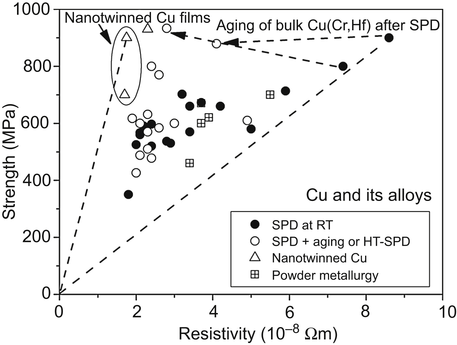
Figure 9.4 Strength versus resistivity for ultrafine-grained pure copper and its alloys. The different processing routes are indicated by various symbols. The strength-to-resistivity ratio values are reflected by the slopes of the lines connecting the data points and the origin of the coordinate system. The materials with the lowest and the highest strength-to-resistivity ratios are indicated by dashed lines. HT-SPD, high-temperature SPD processing; SPD, severe plastic deformation; RT, room temperature. The data were taken from Table 9.2.
In Al-based immiscible systems, such as Al–Ce–La alloys, the very low solubility limits guarantee the formation of secondary phase particles. It was demonstrated for Al–5.4 wt.% Ce–3.1 wt.% La alloy that 20 turns of HPT at RT yielded fragmentation and/or partial dissolution of precipitates [37]. These precipitates are intermetallic phase particles with the composition of Al11RE3 where RE stands for rare earth atoms (Ce and La). During HPT at RT, the grain size was refined from 5.2 μm to 136 nm while the precipitate size decreased from ∼0.15–2 μm to ∼44 nm. In addition, the elongated shape of secondary phase particles became spherical. The average interparticle spacing was 72 nm. The fragmentation of precipitates was accompanied by their partial dissolution, leading to a supersaturated solid solution in the Al matrix. The increase of solute content and lattice defect density in the Al matrix during HPT induced a significant reduction in the electrical conductivity from 50% to 40% IACS. Simultaneously, the yield strength increased from 73 to 475 MPa due to HPT processing. Subsequent annealing at 553 K for 1 h led to a moderate grain growth from 136 to 203 nm, reduction of dislocation density, segregation of RE atoms at grain boundaries, and formation of nanoscale clusters of RE atoms with the size of ∼2 nm. These nanoclusters are distributed homogeneously in the matrix. The size of Al11RE3 secondary particles remained unchanged during annealing. Owing to these changes in the microstructure, the conductivity was improved to 45% IACS while the high value of strength was preserved [37]. It seems that the strengthening effect of nanoclusters in the annealed sample was higher than the hardening of solute atoms in the HPT-processed material, and this difference could compensate the softening caused by the grain growth during annealing. The strengthening of RE clusters is most probably similar to that of Guinier–Preston zones in age-hardenable Al alloys. The purification of the grain interiors yielded the 10% increase in conductivity. Therefore, the annealing at 553 K led to a slight improvement of strength-to-resistivity ratio. At the same time, heat treatment at much higher temperature (673 K) resulted in a strong reduction of grain size from 136 to 385 nm, which could not be compensated by the change of the precipitated microstructure, thereby causing a significant reduction of yield strength to 255 MPa. Although, the conductivity was further improved to 52% IACS, the strength-to-resistivity ratio decreased below the value obtained for the HPT-processed sample (see Table 9.2). It should be noted that the sample processed by HPT at RT and then annealed at 673 K has slightly better conductivity than the initial coarse-grained material (∼50% IACS), and its strength is also much higher (255 MPa) than for the initial unprocessed sample (73 MPa). Fig. 9.5 summarizes the variation of strength and conductivity due to HPT and subsequent annealing in Al–5.4 wt.% Ce–3.1 wt.% La alloy and compares these changes with that observed for pure Al. The much larger reduction of conductivity for Al–5.4 wt.% Ce–3.1 wt.% La alloy compared to pure Al during HPT was caused by the increase of solute content due to dissolution of precipitates in the former material.
In pure metallic materials, the grain boundary relaxation during annealing after SPD processing yields only a minor (about 5%) reduction of resistivity [28]. At the same time, a significant improvement in strength-to-resistivity ratio can be achieved if the majority of HAGBs are substituted by coherent twin faults as the latter interfaces have very low specific electrical resistivity [10,26,27,40]. For instance, in Cu the specific resistivity of coherent twin boundaries is 1.7 × 10⁻¹⁷ Ωm2, which is 20 times smaller than that for a general HAGB (3.4 × 10⁻¹⁶ Ωm2), as shown in Table 9.1. At the same time, coherent twin interfaces possess high resistance to the transmission of dislocations, resulting in a high contribution to strength. Therefore, in pure Cu materials the superior strength-to-resistivity ratio can be achieved by inducing many growth twin faults in the UFG grain interiors, as shown schematically in Fig. 9.6. Nanotwinned UFG microstructures in 5N purity Cu were processed by pulsed electrodeposition [27] and magnetron sputtering [10,26] techniques. In the former and latter methods the thicknesses of the films were ∼100 and ∼1.5 μm, respectively. The grain size and the twin spacing in these films were 70–400 nm and 7–16 nm, respectively. The achieved yield strength at RT was as high as 700–930 MPa, which is about 20 times larger than that for a coarse-grained Cu with the same chemical composition. At the same time, the conductivity of the nanotwinned films at RT was similar to that for a coarse-grained Cu due to the negligible contribution of twin faults. The strength and resistivity of UFG Cu with nanoscale growth twin lamellae are compared with the values obtained for other UFG copper materials in Fig. 9.4.


9.4. Electrical Resistivity of Nanostructured Films
In general, thin films usually have higher resistivity than bulk materials with similar chemical composition. For instance, a sputtered pure polycrystalline Cu film with the thickness of 1 μm exhibited a resistance of ∼2.2 × 10⁻⁸ Ωm at RT, which is about 20% larger than that for pure bulk Cu with similar grain size (∼1.8 × 10⁻⁸ Ωm) [41]. For Cr film with the thickness of 1 μm, the resistivity (∼116 × 10−8 Ωm) was one order of magnitude higher than that for bulk Cr material (∼13 × 10−8 Ωm). In addition, the resistivity of Cr film only slightly increased with increasing the temperature from 4K to RT. These observations can be explained by the very small diameter of the columnar grains (∼30–35 nm) and the high free volume at the grain boundaries in the film. The latter phenomenon is manifested by the higher interatomic spacing at grain boundaries and the lower density of pure Cr films than that observed for bulk material (the density of a Cr thin film was found to be ∼96%–97% of the value of bulk Cr). Therefore, the resistivity of sputtered Cr films is determined mainly by the lattice defects and not by the temperature-dependent electron–phonon scattering [41]. It was suggested that the large interatomic spacing at the grain boundaries in Cr films is caused by large internal stresses. In Cu films, these stresses can relax by twinning in the grain interiors; therefore, the free volume at the grain boundaries is smaller, resulting in only a slightly larger resistivity than in bulk Cu. With increasing film thickness, the resistivity of thin films decreases and asymptotically converges to the resistivity of bulk materials.
Among metallic materials silver has the lowest resistivity (∼1.6 × 10⁻⁸ Ωm at RT). In thin Ag films, the resistivity decreases with increasing film thickness, however, the optical properties (e.g., transmittance) deteriorate for thicker Ag films [42]. This problem can be solved by an appropriate selection of the underlayer material, since the resistivity of Ag films is reduced when the layer is deposited on ZnO undercoats. It was shown that the sputtering conditions of aluminum-doped zinc oxide (AZO) undercoats have a strong effect on the structural characteristics of AZO (e.g., preferred orientation), thereby influencing the electrical resistivity of the deposited Ag films [42]. It was revealed for polycrystalline 20 nm Ag/15 nm AZO layer structure magnetron sputtered on soda–lime–silicate glass at RT that the most effective processing parameter is the applied power. With increasing the power of sputter deposition from 0.3 to 1.2 kW, the electrical resistivity decreased from ∼6 × 10⁻⁸ to ∼4 × 10⁻⁸ Ωm. Simultaneously, plane (002) of the hexagonal AZO undercoat preferably grew parallel to the glass substrate surface, and the overcoated Ag film became highly oriented with its plane (111) parallel to the substrate. The development of this preferred orientation was accompanied by a reduction of Ag film surface roughness. Other sputtering conditions, such as oxygen concentration and pressure in the sputter gas, have only negligible effect on the structure and conductivity of deposited Ag films [42].
Besides the high strength a very low resistivity can be achieved due to the highly twinned grain structure in magnetron-sputtered 5N purity Cu films with the thickness of ∼1.5 μm [10,26]. The Cu layer was epitaxially grown on (011)-orientated single crystal Si substrate. Planes {111} of Cu layer were lying parallel to the film surface; therefore, the relationship Cu ‖Si
‖Si held between the out-of-plane directions of the Cu film and the Si substrate. The in-plane directions are also correlated as Cu‖Si and Cu
 ‖Si [10]. A schematic of Cu film microstructure is presented in Fig. 9.7. A columnar microstructure with high amount of twin faults was developed during deposition. The longitudinal axes of columns (or domains) are lying perpendicular to the film surface (i.e., parallel to the growing direction) while the twin faults inside the domains are lying parallel to the film surface. The vertical domain boundaries were identified as Σ3{112} twin interfaces. Planes {111} coincide in the adjacent columns across the domain boundaries with practically zero misalignment (i.e., the domain boundaries are coherent or semicoherent). Therefore, the epitaxially grown Cu layer can be considered as a single crystalline film with high twin fault density in both parallel and perpendicular to the film surface. It is noted that when the Si substrate was oxidized, the adjacent columns were separated by grain boundaries and the domains have random in-plane orientations [polycrystalline Cu layer with a (111) fiber texture].

The average twin fault spacing in the epitaxially grown single crystalline Cu layer can be tailored with changing the deposition rate [10]. When the deposition rate increased from 0.9 to 4 nm/s, the domain size in plan view (column width) decreased from 146 to 70 nm while the twin spacing perpendicular to the film surface was reduced from 16 to 7 nm. In addition, for high deposition rates (e.g., 4 nm/s) an offset was observed for {111} planes across the {112} domain interfaces. The resistivity of epitaxial Cu layer deposited at 0.9 nm/s was ∼1.7 × 10⁻⁸ Ωm at RT, which is only slightly larger than that for bulk oxygen-free high conductivity Cu (OFHC-Cu). At very low temperatures (10–20 K), where the intrinsic resistivity becomes very small, the resistivity of epitaxial Cu layers is two to three orders of magnitude larger than that for bulk OFHC-Cu. With increasing the deposition rate to 4 nm/s, the resistivity increased to ∼2.3 × 10⁻⁸ Ωm due to the higher density of Σ3{111} and Σ3{112} twin interfaces, as well as the decay of coherency of domain boundaries. It is noted that the latter resistivity is still one order of magnitude smaller than that for polycrystalline nanotwinned Cu films grown on oxidized Si under the same sputtering conditions [10]. The resistivity of a twinned film depicted in Fig. 9.7 can be expressed as:
![]() (9.14)
(9.14)
where dtwin,111 and ηTB,111 are the average twin fault spacing and specific resistivity for Σ3{111} twin interfaces, respectively. dtwin,112 and ηTB,112 are the average twin fault spacing and specific resistivity for Σ3{112} twin faults, respectively. It should be noted that experiments suggested the larger specific resistivity for Σ3{112} interfaces. As a consequence, the experimentally determined value of the average specific twin fault resistivity in sputtered Cu films increased from ∼1.5 × 10⁻¹⁷ to ∼3 × 10⁻¹⁷ Ωm2 with increasing the deposition rate, which can be attributed to the contribution of semicoherent Σ3{112} twin interfaces developed at higher sputtering rates. The higher deposition rate also caused an increase in hardness from 2100 to 2800 MPa at RT. Therefore, the strength-to-resistivity ratio of sputtered Cu with high density of nanotwins reached a superior value of ∼4 × 10¹⁰ MPa/Ωm, which did not change considerably with the variation of deposition rate. Similar high strength-to-resistivity ratio (∼5 × 10¹⁰ MPa/Ωm) was obtained for nanotwinned 99.998% purity Cu film processed by pulsed electrodeposition (see Table 9.2), although the microstructure was very different from the epitaxially grown sputtered film [27]. The as-deposited Cu film was polycrystalline with a thickness of ∼100 μm and consisted of irregular-shaped grains with random orientations. The microstructure resembles to that depicted in Fig. 9.6. The grains had a wide distribution with an average size of 400 nm and contained a high density of twin faults with a mean twin-fault spacing of 15 nm. Similar grain size was achieved in 99.96% purity Cu by 16 passes of ECAP at RT but without large amount of twin faults in the grain interiors [19]. The twin faults inside the grains of the electrodeposited film increased the strength by a factor of 2.6 without significant reduction of conductivity.
It was shown in Section 9.3 that secondary phase body-centered cubic Cr nanoparticles in UFG fcc Cu matrix improve the strength-to-resistivity ratio significantly, since they increase the strength much more strongly than the resistivity. This beneficial microstructure in bulk materials can be achieved by sequential SPD and annealing processes. It is noted that Cu and Cr are practically immiscible in solid state. Applying sputtering techniques, Cu/Cr multiphase microstructures with improved strength-to-resistivity ratio can also be produced in thin films [41,43]. For instance, a Cu/Cr multilayer with 1 μm film thickness and 50 nm layer thickness exhibited a very high strength of 2000 MPa and a resistivity of ∼7 × 10⁻⁸ Ωm at RT. The strength-to-resistivity ratio was ∼2.9 × 10¹⁰ MPa/Ωm, which is almost as high as the best value obtained for bulk copper alloys (∼3.3 × 10¹⁰ MPa/Ωm detected for Cu–0.7wt.% Cr–0.9wt.% Hf processed by five turns of HPT at RT and subsequently annealed for 1 h at 773 K, see Table 9.2). With decreasing layer thickness in Cu/Cr multilayers, the resistivity considerably increases due to the enhanced contribution of layer interfaces [41]. For layer thickness of 150 nm the resistivity was ∼5.5 × 10⁻⁸ Ωm at RT, which increased to ∼27.5 × 10⁻⁸ Ωm when the layer thickness was reduced to 1.25 nm. At the temperature of 4 K, the resistivity is smaller than that at RT with a value of 2.5–3.5 × 10⁻⁸ Ωm. This difference decreases slightly with the reduction of layer thickness. As the resistivity of Cu/Cr multilayers is much smaller than that for Cr thin films, it can be concluded that the resistivity is determined mainly by the current flow through the Cu layers, which is strongly influenced by the scattering at interfaces, and the Cr layers carry only a small fraction of current [41]. The ratio of the resistivities measured at RT and 4 K is much smaller (varying between 1 and 3) for Cu/Cr multilayers than for Cu thin films (about 8), which suggests an enhanced role of defects (primarily Cu/Cr interfaces and grain boundaries inside the layers) in conductive electron scattering. The strength, resistivity, conductivity, and strength-to-resistivity ratio for Cu/Cr multilayers with different layer thickness values are listed in Table 9.3. Fig. 9.8 shows that the strength-to-resistivity ratio strongly decreases with the reduction of layer thickness since interfaces and grain boundaries in Cu/Cr multilayers are more effective in the deterioration of conductivity than in the improvement of strength.
Table 9.3
Grain size, mechanical strength, conductivity in International Annealed Copper Standard (IACS), resistivity, and strength-to-resistivity ratio measured at room temperature (RT) for Cu/Cr multilayers with different layer thicknesses. The strength is calculated as one-third of the hardness [41,43]
| Material and processing method | Grain size (nm) | Strength (MPa) | Conductivity in IACS (%) | Resistivity (10−8 Ωm) | Strength-to-resistivity ratio (1010 MPa/Ωm) |
| Cu–Cr multilayer sputtered at RT, layer thickness: 50 nm | 32/10 (Cu/Cr) | 2000 | 24 | 7.0 | 2.9 |
| Cu–Cr multilayer, sputtered at RT, layer thickness: 25 nm | – | 2070 | 18 | 9.5 | 2.2 |
| Cu–Cr multilayer sputtered at RT, layer thickness: 10 nm | 9/7.5 (Cu/Cr) | 2330 | 11 | 15 | 1.6 |
| Cu–Cr multilayer sputtered at RT, layer thickness: 5 nm | 5/5 (Cu/Cr) | 2330 | 9 | 20 | 1.2 |
| Cu–Cr multilayer sputtered at RT, layer thickness: 2.5 nm | 2.5/2.5 (Cu/Cr) | 2400 | 6 | 27.5 | 0.9 |


..................Content has been hidden....................
You can't read the all page of ebook, please click here login for view all page.