
Chapter 6. Building Hardware
Hardware: the part of a computer that you can kick.
—Anon.
Before we get into the designs later in this book, let’s spend some time looking at how you would produce the physical machine. Building a computer that doesn’t work is really easy. You may have a perfect design and flawless code, but ignore the physical environment in which the machine will exist, and you’ll have built yourself a very intricate paperweight. In this chapter, I’ll also show you how to lay out a circuit board (and what to be careful of) and how you debug your hardware. We will look at how you physically produce a computer by laying out the design for the ATtiny15 computer, presented in Chapter 15. I’ll assume that you’re hand-building in small quantities and target the discussion accordingly. What I present here is not the state of the art in circuit board design or assembly, but guidelines for “cottage-industry” computer production. If you need to make production runs of hundreds of thousands, either you already know what you’re doing (and can skip this section) or you need to talk to a professional.
Tools
To design and build an embedded computer, you have to start with the right tools. The first thing you will need to design a computer is another computer. It’s a chicken-and-egg problem. You will need software tools to create the design (schematic and circuit board layout), and you will need software tools not only to write your code, but also to download it into your embedded target machine.
Development Kits
When you’re developing your embedded system, it’s best to start with a development kit from the processor’s manufacturer (Figure 6-1).
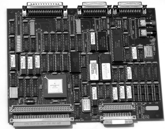
A good development kit will not only provide you with a working example of the machine you’re trying to build (and upon which you can test your code), it should also include a nice Integrated Development Environment (IDE). The IDE will have a windowing editor, a debugger, a simulator too if you’re lucky, an assembler, and hopefully a C compiler as well. The kit should also come with cables and tools for downloading code to the processor and circuit schematics so you can see what a working machine should look like. However, treat the schematics with a small degree of caution. Some (but not all) semiconductor manufacturers farm out the design of their development systems to small, external companies. Some of these companies do a fantastic job, while others seem to employ stray chimpanzees as design engineers. In the latter case, the development system will work, but only through a miracle and by the grace of the digital gods. So, treat the schematics as a rough guide only. They are not always the best example of how a system should be designed.
To use the IDE, you will need a desktop computer, and here lies the bad news. Almost without exception, the IDEs will run on only one platform and under only one operating system. No prizes for guessing which one. So, if your preferred environment is a Unix workstation, generally you’re out of luck. While the gnu tools are great, they don’t support a lot of the smaller processors, and sometimes you just have to resort to the chip maker’s IDE to download code into your target computer.
Development kit prices range from free (if you’re at the right place at the right time) to many tens of thousands of dollars for some of the really high-end and exotic processors. For most embedded-type processors, you can expect to pay somewhere between $50 and $300, depending on the chip, the manufacturer, and their current whim. For the time they will save you, it’s probably worth investing in one.
Measurement Tools
For the systems described in this book, the minimum debugging tools you will need are a multimeter (Figure 6-2) and an oscilloscope .
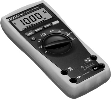
A multimeter allows you to measure current and voltage, but, more importantly, it also allows you to do a continuity test between two points (and verify that there is a physical, and therefore electrical, connection). However, do not do continuity tests if there are sensitive components in your system. The continuity test may cause them damage.
Warning
Don’t assume that just because a signal is present at one end of a trace that it is present at all points along the trace. Check everywhere with an oscilloscope probe, and use your multimeter to confirm that signal paths are connected properly.
An oscilloscope (Figure 6-3) allows you to view waveforms within your system, and, as such, it is your principle debugging tool. Oscilloscopes range from the crude and ancient to the expensive and sophisticated. While you don’t need to spend $100k on an oscilloscope, you will need one that can accurately view waveforms. That rules out the $20 antique you picked up from Mr. Gorsky’s garage sale down the road.

You will need an oscilloscope of sufficient bandwidth to view the signals within your computer. There’s no point using a 20 MHz oscilloscope to look at a 100 MHz system clock. The oscilloscope simply won’t see it, and therefore neither will you. The higher the bandwidth, the more you will see. While you may think that the signals of a 4 MHz embedded processor might not require a 100 MHz oscilloscope, that oscilloscope will allow you to see the rising edges of the waveforms as rising edges (and not just vertical transitions) and view miniscule timing differences that may be having an adverse effect. It will also allow you to see fine spikes of noise or ringing on your signal lines, which may be adversely affecting your machine.
I really like the (relatively) low-cost Tektronix oscilloscopes for debugging embedded systems. HP and others also make nice units. If you’re serious about developing embedded hardware, it’s worth investing in one. Keep an eye out for startup companies going under—you may be able to pick up some great test gear going cheap!
When using an oscilloscope, it is critical that you connect the ground clip of the probe to a ground connection close to (or better, on) your embedded system. Without this, your measurement of the signal will be affected by ground loop problems, and you will not get an accurate reading. You’ll spend ages chasing phantoms, all the while missing the real problem.
Logic analyzers (Figure 6-4) are very expensive tools that allow you to monitor and diagnose a multitude of digital signals simultaneously. They are essential for developing high-speed and complex systems (especially those with buses), but you should be able to get by without them for the simpler designs in this book. Certainly, for a completely self-contained microcontroller, a logic analyzer is of no use at all.

In-Circuit Emulators
Another development tool is the In-Circuit Emulator (ICE ). This is a small module with the same footprint as the processor, which is placed into the target system under development. Under the control of software executing on a PC and emulating the embedded processor, the ICE behaves just as the processor would in-circuit. This allows you to interactively debug your hardware and software. This can be especially useful in systems based on self-contained microcontrollers, where it would be otherwise difficult (impossible) to get to the system internals.
Some ICEs are better than others, and, as with everything, you get what you pay for. For really sophisticated tools that closely match the timing and electrical characteristics of the processor, expect to pay big bucks. Cheaper systems will emulate the processor’s operation but will do so with completely different signal timings. Also, for each processor type around which you develop systems, you’ll need a different ICE.
Some engineers use ICEs heavily during their embedded system’s development process. Call me a heretic, but I get by quite well without them. The catch with an ICE is that no matter how good a particular tool is, it is never going to be exactly like the real thing. There will always be some slight difference in the electrical characteristics or in the timing. The engineers at Boeing have a saying: “Test what you fly; fly what you test.” In other words, there’s no substitute for the real thing.
Construction Tools
Finally, you’ll need a good soldering iron, some side-cutters, a pair of pliers, and other construction tools. Don’t use the same pliers you use to build your fence; get some high-quality pliers with very fine jaws. I have six pairs of pliers, all suited to very fine work, and each is slightly different. I also have a set of jeweler’s tools, useful for very fine and delicate assembly work. If you can afford it, a quality binocular microscope is very useful not only for construction, but also for verification of the final assembled circuit. Figure 6-5 shows just a sampling of some of the tools I regularly use during construction.

Soldering
Soldering is very easy to do well, and very easy to do badly. The basic skills are simple to learn. Becoming a wizard with the soldering iron is not hard to achieve.
Warning
Safety First
The most important thing to note about solder is that it contains lead. Therefore, all soldering should be done in a well-ventilated work area, and avoid breathing the fumes! After soldering, wash your hands, especially before eating!
Solder can splatter, so always wear protective eyewear and clothes.
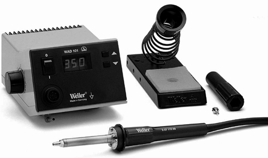
Solder is a metal alloy with a relatively low melting point. It is used to bond components to circuit boards and forms a conductive join. Solder is available as either strand solder (like a spool of wire) or solder paste (out of a syringe). There are two basic categories of soldering tool: the standard soldering iron and the rework station . Weller (http://www.cooperhandtools.com/brands/weller) and Hakko (http://www.hakko.com) both make excellent soldering tools. Weller has kindly supplied photographs of some of its products so you may see examples of each type of tool.
A soldering iron (Figure 6-6) is used with strand solder to mount through-hole components. Note the sponge used for cleaning the iron’s tip. The sponge should be kept very wet at all times, and the iron’s tip should be wiped regularly. (Don’t squeeze out the sponge as you would a dishcloth. It needs to be really wet, although not drenched.)

There are many different tips available, depending on the type of work you are doing and the temperature at which you want to solder. When the iron is cold, it is a simple matter to unscrew the tip and replace it with another. Tips eventually wear out and need replacing. Spare parts are readily available from most electronics suppliers.
Warning
Never remove the iron’s tip when the iron is on. The tip contains a sensor that controls the heating element. Removing the tip will cause the iron to overheat and may damage the unit.
Also never leave a soldering iron turned on for extended periods when it is not in use. Doing so will reduce the life of the tool.
Always ensure that the iron’s tip has a fine coating of solder, as this prevents oxidization and prolongs the life of the tip. As you work with the tip, it will become discolored. Simply feed some strand solder onto it when it is hot and wipe this excess off on the sponge. This will ensure that your iron’s tip is kept in good condition. A well-cared-for tip will allow you to solder successfully. A poorly maintained tip will make the job of soldering very difficult indeed.
Rework stations (Figure 6-7) blow heated air through a small nozzle and are primarily used with surface-mount components and solder paste. However, it is relatively straightforward to solder some surface-mount components using a standard soldering iron. You don’t necessarily need the more expensive rework stations , although they do make a lot of surface-mount work easier. Regardless of whether you invest in a rework station, you will always need a conventional soldering iron. There are many components (such as through-hole connectors) that require a standard iron.
Integrated stations that combine both standard soldering tools and hot-air guns are also available. Figure 6-8 shows a Weller WRS3000ST unit.

For working on ball-grid array (BGA) packaged chips , you’ll need access to a rework station like the Weller WQB 3000 (Figure 6-9). These allow you to accurately place components and successfully bond the many hundreds of solder balls (pads) under a BGA. If you can’t afford a machine like this, there are companies that specialize in assembling electronic systems. They will be able to mount your components to your circuit board for a price.

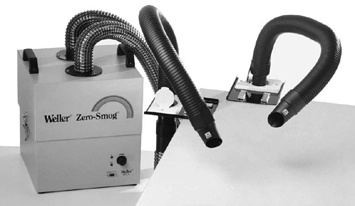
Solder fumes are toxic, and prolonged exposure to them is bad for your health. When soldering, ensure that your work area is well ventilated. It may also be worth investing in a fume extractor, such as that shown in Figure 6-10.
How to Solder
The key to soldering well is to control the heat and the amount of solder that flows onto component pins. Too much heat can damage a component (especially sensitive integrated circuits) and can overheat the solder as well. Read the datasheets to determine the maximum temperature (and duration) that the components can take and ensure that your soldering does not exceed this. Variable-temperature irons allow you to set the temperature, thereby avoiding overheating. The tip of your soldering iron should be thin, allowing you to do fine work. An old-style iron with a large, bulky tip (intended for electrical work) is not appropriate for soldering electronics.
Warning
Whenever you solder your PCB, make sure it is not powered! The tip of a soldering iron is grounded, and touching this to a pad with volts on it is not a good idea!
Similarly, when inserting or removing socketed components, ensure that the system is powered down. Most semiconductors do not appreciate being plugged into a live system.
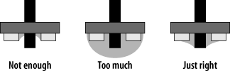
There should be enough solder to make a good contact, but not so much that it bulges up or, worse, shorts a neighboring pin (Figure 6-11).
Tip
During the Apollo/Saturn missions, NASA found that teaching its technicians the correct way to solder saved several hundred pounds in takeoff weight.
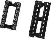
When soldering through-hole components (such as DIP-packaged chips or connectors), place the component into its hole and ensure that it is mounted correctly and sits flat. To begin, solder one pin only, then check that the component is still seated correctly before doing the remaining pins. With the iron in one hand and a thin strand of solder in the other, bring the two together such that they meet at the pin to be soldered. Within a second, the solder will flow around the pin and you will have a good join. As soon as the solder begins to flow, remove both the iron tip and the solder strand. If you are using DIP chips, rather than soldering the chip directly into the circuit, solder a DIP socket instead. This allows you to easily remove/replace the chip if you have to, without the inconvenience (and frustration) of desoldering. Figure 6-12 shows a machined socket (left) and a “dual-wipe” socket (right). Machined sockets, while they cost more, are more reliable and will last longer.
Common mistakes when soldering are to heat the component pin for several seconds before applying solder (causing the component to become too hot) or to apply the solder directly to the iron and then dab the molten solder onto the pin.
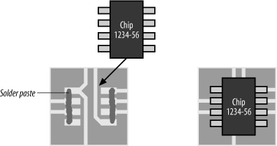
Soldering surface-mount components requires a different procedure. If you’re using a rework station, you will need to use solder paste. This is sold in a large syringe. Solder paste dries out easily inside the syringe, so ensure that you seal the end when it is not in use. Before soldering a surface-mount chip, place a thin squirt of solder paste along each row of pads on the PCB. If there is too much paste, it can flow under the chip and create a short, so keep the application light. You can always add a small quantity later. Place the chip onto its PCB pads and ensure that it is lined up correctly; then use the rework station to apply heated air (Figure 6-13). Too much airflow will either shift the chip off its correct orientation or, worse, blow solder paste underneath. Since solder paste is electrically conductive, this is not a good thing. Too little heat will result in poorly soldered joints, whereas too much heat can easily overheat and damage the chip. It is something of an art to get it just right, so it’s best to do considerable practice before tackling the real thing.
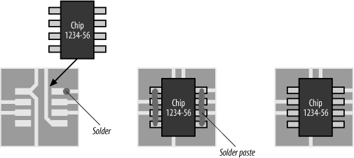
Surface-mount chips can also be soldered using a standard iron, although it’s not recommended for really finely spaced chip pins. Unlike the technique with the rework station, solder paste is applied after the chip is in place. To begin, before putting the chip on the PCB, use the iron and either strand solder or solder paste to place a small dab of solder directly onto one of the pads where the chip is to be mounted. Place the chip in position, aligning it carefully, and then use the iron to heat the pin resting on the solder dab. The dab will melt and fix the chip in place. Check the alignment again to ensure that the chip did not shift. If it did, reheat the pin again, and carefully shift the chip as appropriate. Once you are happy with the alignment, place a thin squirt of solder paste down each row of pins, as far from the edge of the chip as possible. Too much paste will flow between the pins, creating shorts, so keep it light. Gently and quickly run the tip of the soldering iron down each row of pins. The solder paste will melt and flow as you go, bonding the chip to the PCB (Figure 6-14).
Solder is a metal alloy and incorporates a flux to assist flow. When heating the solder, it is common for the flux to separate and flow out onto the surrounding PCB, leaving a thin brown residue. Excess flux can be removed using special solvents, available from most electronics hobby stores and suppliers. Flux removers can be nasty stuff, so keep them away from skin and plastics and use them in a well-ventilated work area. Flux residue is removed for cosmetic reasons only, making your circuit boards look more professional for your customers. However, as it is for appearances only, and since flux solvents are not good for either you or the environment, if you can avoid using them, please do so.
Tip
A Note on Pronunciation:
If you are a resident of North America, solder is pronounced “sodder.” If you live anywhere else in the English-speaking world, you will pronounce it as “sol-der.” So Americans, be advised that if you say the word as “sodder” to non-Americans, they may not know what you’re talking about. Instead, they may think you’re confessing to strange and unspeakable acts, rather than talking about bonding metals together.
So, with all that in mind, what are your options for construction? There are several ways of fabricating a computer (or any other circuit). Let’s take a look at them.
Quick Construction
It is possible to build very simple circuits by just soldering the components together in free space. For example, the leads of a watch crystal can be soldered directly onto the pins of the processor, with the crystal lying across the top of the processor. Wires are soldered onto the pins bringing in ground and power, and connecting the processor’s I/O to the outside world. This technique is variously referred to as a rat’s nest, bird’s nest, or “what the hell is that?" (Figure 6-15).

This is a quick-and-dirty method, useful for rapid prototyping of extremely simple circuits. It’s not really recommended, but you can get away with it in a pinch. Don’t try it with anything that is even slightly complicated or running at any reasonable speed. If you do, you’ll spend more time debugging the construction than debugging the actual design or code!
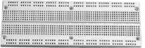
Breadboarding
Breadboards are plastic blocks with arrays of electrically connected holes (Figure 6-16). They are designed to hold DIP (Dual Inline Package) integrated circuits and discrete components. The term “breadboard” dates back to the olden days when valve radios were constructed on a base of solid wood (a cutting board for bread). The term has stuck, and the modern breadboard can still be found in electronics hobbyist stores, and even the occasional university teaching lab.
As a general rule, breadboards are bad news, and their use should be avoided at all costs. (Think of them as the hardware equivalent of COBOL.) They suffer from excessive capacitance, crosstalk, and noise susceptibility and, as such, are completely inappropriate for microprocessor system construction. It’s hard enough trying to debug microprocessor hardware and software (together) without the additional complications that breadboards can add. Breadboards can also suffer from mechanical failure after extended use, leading to short circuits. Circuit interconnections on a breadboard are done with small sections of wire. These make great little antennas and will pick up every scrap of stray electromagnetic radiation, channeling it straight into your circuit! Microprocessors don’t, as a rule, like “Classic Rock FM” modulated onto their data bus.
Using a breadboard is not the way to construct a robust and reliable system. If you really must, you could probably build the ATtiny15 or PIC12C805 computers (discussed in later chapters) on a breadboard, using their internal RC oscillators. But I’d advise against using breadboards for anything that uses a crystal or that has any fast-switching digital signals. While it is possible to build very low-speed microprocessor systems and general digital circuits on breadboards, try not to. There be dragons!
Wirewrapping
Once common as a construction technique, wirewrapping is now relatively rare. It is intended for use with DIP-packaged integrated circuits, mounted into sockets with long pins (0.6”). Figure 6-17 shows an embedded computer built as a student project using wirewrapping.

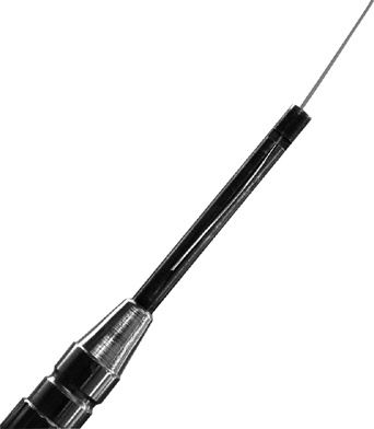
Special tools, known as wrapping tools , allow you to quickly and efficiently wind thin wire around the pins. Figure 6-18 shows a low-cost, hand (manual) wrapping tool on the left and a wire stripper on the right. Automatic tools are also available.
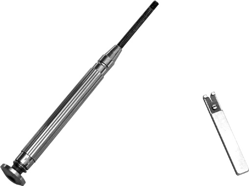
The wire stripper is used to remove the insulation from fine-gauge wire (Figure 6-19).
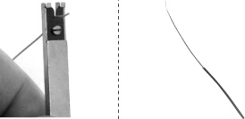
The stripped wire is then inserted into the notch of the wrapping tool (Figure 6-20), and the tool is then placed over a socket’s pin. The tool is rotated so that the wire is wound onto the pin.
The pins are square in cross-section, and wrapping a wire around a pin forms a cold weld --a tight electrical connection between wire and pin with no soldering (Figure 6-21). In this way, a circuit is constructed by individually wiring point-to-point each connection within the system.

Figure 6-22 is a photo of the underside of a wirewrapped computer (in this case, a LISP engine designed and built by Peter Paine). Note the square cross section of the pins and the tightly wound wires.
Wirewrapping is a very fast prototyping technique and is very robust and reliable. In the early days, NASA used wirewrapping for the construction of spacecraft avionics, and many mainframe computers were also built using the technique. Wirewrapping is good for prototyping (especially if you’re unclear as to the final form of the design and expect to make lots of changes to the hardware) or for building one-off designs. If you intend to make more than one computer based on your design (and you probably will), then skip wirewrapping and do it on a printed-circuit board.
Printed-Circuit Boards
Printed-circuit boards (PCBs) are epoxy-bonded fiberglass sheets plated with copper. The copper plating is etched away, leaving tracks (traces) that form the interconnections of the circuit (Figure 6-23). PCBs are very reliable and are the only realistic option if you intend to produce more than one system. It is possible to etch your own PCBs, but commercial PCB production isn’t that expensive, and it is worth the cost to get professionally produced boards.

EDA (Electronic Design Automation) software is used to create the schematic and PCB design. The most popular EDA software comes from Mentor Graphics (http://www.mentor.com) and Protel (http://www.protel.com). There is also a gnu (http://www.gnu.org) PCB editor, called PCB, which is freely available. Such programs normally come with several tools, allowing schematic entry, netlist generation (a list of what needs to be connected to what), PCB layout, manual routing (making the connections), and autorouting. There’s a great temptation to use autorouters, as they simplify the process of generating the PCB by getting your workstation to do the hard work of routing. However, I prefer to lay out the circuit board myself. (I’ve seen some autorouters make a real mess of a design.) Routing the board manually can take a long while, but it is often worth the extra effort. It can also be very absorbing, much like spending hours in deep meditation. (It’s very Zen.)
PCBs can be either single-sided (one layer), double-sided (two layers), or 4-layered, 6-layered, 8-layered, 12-layered, or more. The more layers you have, the easier it is to route your interconnections, but the costs of fabrication go up considerably with extra layers. Further, it’s much easier to debug a 2-layered board than a 12-layered board. An advantage of using additional layers dedicated to power and ground planes is that your system will have greater noise immunity. While not so critical for slow 8-bit systems, they are mandatory for high-speed computers.
Multilayered boards will be plated through , meaning there will be metallic connections through the holes in the board, connecting traces of different layers together, as appropriate. A solder mask is the (normally) green coating on circuit boards, and it prevents solder from flowing between pads and tracks during construction. It is possible to order commercial PCBs without plating through and without solder mask, but the small amount you will save is not worth the hassle.
The overlay layers (also known as silkscreen layers ) are painted on and contain labels (such as “R30” or “RAM4”) used during construction and repair to show component placement. The overlay layers are optional. If the boards are to be manually populated with components by someone else, the overlay layers are helpful during construction. If you’re building them yourself, then you can easily do without the overlays and save a few bucks.
Tip
A useful trick if you’re skipping the overlays is to place component information as text on the copper layers. Just be sure to avoid making contact with the circuit tracks!
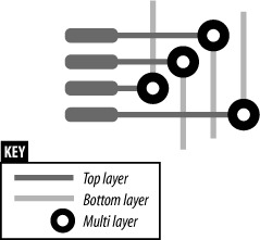
The external copper layers are called top and bottom (no surprises there). Traditionally, the top layer was called the component layer , and the bottom layer was called the solder layer , since components used to be mounted on top and their pins soldered underneath. However, many modern circuit boards place surface-mount components on both sides and are soldered on both sides. Thus, the terms “component layer” and “solder layer” are seeing less use.
There are also internal copper layers for multilayer boards, mechanical layers (indicating any special physical features), the keepout layer (showing the actual PCB shape), and others. In four-layer boards, it is common practice to use the outer layers for signals and the internal layers for power and ground. This not only provides shielding, but also minimizes the current-loop area, thereby giving your design greater stability.
The five types of objects that can be placed on a copper layer are tracks, individual pads, components (arrays of pads grouped together), vias, and fills.
Tracks are used to interconnect components. Track width is expressed in thousandths of an inch (“mils”) or in millimeters (mm). Tracks can be of varying thickness, and often a PCB will have different widths for different tracks. The fatter the track, the more current it can carry. The thinner the track, the easier it is to fit more tracks in a given space, and, therefore, the easier it is to route the PCB. As a general guide, Table 6-1 gives a list of the current-carrying capacity of different track widths for a temperature rise of +10°C.
|
Mils |
mm |
Amps |
|
8 |
0.2 |
0.5 |
|
12 |
0.3 |
0.75 |
|
20 |
0.5 |
1.25 |
|
50 |
1.25 |
2.5 |
|
100 |
2.5 |
4 |
|
200 |
5 |
7 |
|
325 |
8.12 |
10 |
Check with the company doing your PCB fabrication as to what tolerances it can manufacture. There’s no point in doing a PCB with 4 mils tracks if your local PCB fab company can only etch as small as 8 mils.
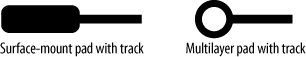
Pads are used to mount component pins, and they can be round, rectangular, or oval. They consist of a hole and a copper surround. A pad for a component in a DIP, for example, will be a multilayered pad, meaning that the pad appears on all copper layers, and the hole is drilled through the entire PCB. A surface-mount component will have pads that appear on one layer only (Figure 6-24). An array of pads grouped together to form a component package is known as a footprint . Surface-mount components have holes of zero diameter (in other words, they aren’t drilled). These components are small, with “gull-wing” pins that mount flat on the PCB. They are less susceptible to noise interference than the older DIP-style of packaging. However, DIP (through-hole) components may be easily mounted in sockets and are therefore easily removed during debugging. DIPs are sometimes preferable (although not always feasible) during early development, while surface-mount is the only option for production. Surface-mount components radiate less noise and are less susceptible to external interference. Conversely, DIPs have terrible noise-related characteristics.

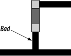
Tracks entering a pad should “aim” directly for the pad center, as shown in Figure 6-25, and not as in Figure 6-26.

When specifying the pads for a component, ensure that the pad size is large enough to accommodate the pins and to allow enough space on which to solder. Also ensure that the holes (for through-hole components) are large enough to take the pins. A standard DIP pin will happily go into a 0.7 mm hole, while a DB connector requires 0.9 mm holes for the signal pins and 3 mm holes for the mounting pins.
Warning
Don’t assume that the libraries of predefined components that came with your PCB CAD software have the pads, spacings, or holes right. It is not uncommon for CAD libraries to get it very wrong. (No kidding.) There’s nothing worse than getting a beautiful new PCB back and finding that you can’t mount the components! So, check and recheck.
When routing tracks around pads, ensure that there is sufficient clearance, as shown in Figure 6-27. Tracks should always change direction by 45-degree turns. Some PCB editing programs allow you to do a design rule check (also known as an electrical rule check ) to ensure that correct clearances are maintained and that there are no potential shorts. (It’s no guarantee that there won’t be a problem, but it’s a start!)

Avoid close passes and right-angle turns, as shown in Figure 6-28.

Closely spaced pads on surface-mount components can present a problem. Often the tracks leaving a surface-mount device are too close together to easily route tracks. The solution is to fan out the tracks, thereby giving greater spacing. This is shown in a simplified form in Figure 6-29.

Vias are used to connect tracks on different layers together (Figure 6-30). They are, in effect, little pads. Vias can either be through-hole vias appearing on all layers (Figure 6-31), or blind or buried vias, appearing only on the layers they are interconnecting and on intermediate layers. Making the vias as small as possible aids in routing the PCB, but check with your PCB manufacturer as to how small you can go. Remember to ensure that the outside diameter of the via is sufficiently bigger than the hole, such that the entire via is not drilled out during fabrication. If space permits, a useful trick is to make the vias with 0.4 mm holes. That way, if there is a bug in the PCB layout or a manufacturing fault, you can use the vias to solder in wire-wrap wire and manually make (or remake) a connection.

Fills are used to provide shielding to certain sections of the PCB, and also for circuit paths that carry a lot of current. It is common to place ground fills in and around analog sections of the circuit to isolate them from digital crosstalk.
Laying Out a PCB
The first thing to note when laying out a PCB is that someone (or some robot) is going to have to assemble it. As tempting as it might be to cram everything into the smallest space possible, remember the limitations of whoever (or whatever) will be building it. That’s not to say you should make the PCB as big as possible—just be realistic. Also, don’t bring components and tracks right to the edge of the PCB. Leave a spacing of 5 mm (200 mils) around the outside. If your PCB is to go inside a case, or be mounted in some way, make sure you have the dimensions correct and don’t forget to add mounting holes.
There are two schools of thought in placing components (especially integrated circuits) on a PCB. The first is that all components should be placed with the same orientation. For instance, the “pin 1” of each chip should point to the upper lefthand corner of the PCB. This simplifies populating (or stuffing) the board with components, especially if this is to be done by a contract manufacturer in an automated process. Having varying orientations may add to the expense of production if you’re not hand-assembling the boards yourself. Some people also think that this makes a board look neater.
The second school of thought is that you orientate the chips so as to optimize the routing process. The pinouts of different chips are not necessarily conducive to uniform orientation, and spinning one chip 90 or 180 degrees to its neighbor may greatly simplify the routing of tracks between the two. This can lead to a smaller board size, fewer vias, and shorter track lengths. This then results in lower PCB cost, less noise, less crosstalk, and better noise immunity, which is especially important in higher-speed systems.
Whatever you decide about orientation, group related components together. Put the voltage regulator and its support components near the power connector. Any analog circuitry (such as sensors or amplifier circuits) should be as far from the power connector and its support components as possible. By placing chips into functional groups, routing is made easier. This may seem like obvious stuff, but it’s amazing how often it’s ignored.
The clocks and high-speed signals should be routed first, to ensure that they take the most direct path possible from source to destination. Where appropriate, place shielding (fills) to isolate these signals from other parts of the PCB. This should be done prior to routing other connections; otherwise, there may not be sufficient space later on. In particular, tracks should never be routed under or around crystals, oscillators, or any clock-generation circuit, and these components should be isolated by fills (connected to ground) from the rest of the circuit. Crystals should lie flat against the PCB (rather than being mounted vertically), and a ground plane should be placed under them to shield from emissions.
For high-speed signals, make sure there is a ground return path close to the track so that the current-loop area is minimized. Allow as much space as possible between high-speed tracks. Having two rapidly changing signals in close proximity will result in crosstalk, and this will cause unreliable operation. Every track has an inherent impedance (resistance); although small, it can affect the transmission of fast signals. In particular, a via or sharp corner represents a change of impedance along the track, and this can cause signal reflections. Therefore, it’s important to keep the number of vias to an absolute minimum and avoid right-angle turns in tracks. If you need to make a track turn 90 degrees, use two 45-degree turns in succession.
In high-speed systems, you need power and ground planes that are continuous. In other words, you need planes that cover the entire PCB with no breaks. Any break in the power or ground plane makes the current-loop area larger, and this can increase inductance and radiation. This means that for high-speed systems, you really need to use four or more layers on the PCB. For low-speed microcontrollers, you can get by without separate planes or by providing fills in and around components on the signal layers.
When routing buses (such as data and address), keep the tracks running parallel if possible (Figure 6-32). This is bad practice for clock signals, since it can induce crosstalk in neighboring tracks, but is appropriate for buses. The reason is that bus signals will change state together and will then hold that state until the next transaction. The device receiving the bus signals will sample their state only when they are stable (unchanging). Since crosstalk is generated when a signal state changes, running parallel buses is not a problem. By keeping the bus tracks parallel, the signals travel approximately the same distance for each track. A track that takes a different path completely will have a trace-length mismatch, and this can increase signal skew, in which the time it takes for a signal to propagate is shifted. This can adversely affect signal quality in high-speed systems.

Stubs are short tracks that leave a main track to connect to a component (Figure 6-33). A stub represents an impedance mismatch for a signal and can result in reflections. A better way is to place the component such that the pad lies on the primary signal track (Figure 6-34).

All power and ground traces should be as fat as possible, and, if feasible, separate power and ground planes (layers) should be used. The power ground (ground coming in with the power supply) should be separate from the signal ground or digital ground (the ground running to all your chips), and both should be separate from the analog ground (the ground for your analog components), if one is present. They should all be connected together, but only at one point. This helps isolate the digital and analog sections from each other’s noise, as well as from the power-supply noise. Decoupling capacitors should be as close as possible to each power pin of each integrated circuit. Figure 6-35 shows two components on a two-layer PCB, with power and ground tracks routed horizontally through the middle and decoupling capacitors placed close to the power pins.

Tip
A very useful and simple idea is to place a single pad in the middle of a ground plane (or fill) off to the side of the board. Solder in a post (or even a wirewrap pin), and use this to connect the ground lead of your oscilloscope probe. This can make the debugging process a lot less awkward. You must always use the ground lead of your oscilloscope probe. Without it, you can’t get an accurate picture of the timing and voltages of your signals. (Voltage is the potential difference between two points, so you must have a reference.) It’s very important.
So, with all that in mind, let’s create a simple circuit board for an AVR computer. This design is covered in detail in Chapter 15, but for the moment, we’ll just use it as an example so that we can see the process of producing a printed-circuit board.
We start with the schematic (Figure 6-36). This design brings together the voltage regulator circuit (top), the AVR processor (left) with a status LED (far left), and the in-circuit programming interface (right).
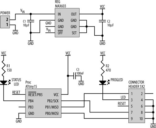
Note that no connection is made for pin 2 of the connector. This is the +5 V supply provided by the in-circuit programmer. Since our embedded system has its own supply of +5 V (VCC), the external source is not required. (If we were building a 3 V version of this computer, then we would need to use the programmer’s +5 V supply, and we’d have to disable the output from the voltage regulator during programming.)
From this design, we use our schematic editor to generate a netlist file, which tells the PCB editing software what interconnections need to be made.
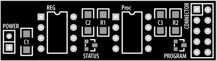
Importing the netlist file into the PCB editor automatically loads the component footprints. These are manually rearranged to provide optimum placement, ensuring the shortest track runs between components (Figure 6-37). Note how related components are placed together, such as the voltage regulator, C1, C2, and the power connector. The silkscreen (overlay) layer shows the outline of the components, as well as the component labels. In this example, surface-mount components have been used for the resistors, capacitors, and LEDs, while the two integrated circuits are DIPs. Note the three-pad triangular LEDs (“STATUS” and “PROGRAM”). Only two of the pads are connected to the internal LED; the third is unused. This tiny circuit board measures just 2” by 0.6”.
Once you’re satisfied with the component placement (and this may need tweaking as you go), the connections are routed. Figure 6-38 shows the PCB with manually routed connections. In this case, the overlay layer has been “turned off” for clarity. Note the use of fills for power and ground connections. For such a simple circuit, operating at low speed with no external system buses, the PCB layout is relatively trivial.
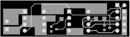
Just for comparison, Figure 6-39 shows the same board, but this time using the EDA software’s autorouter to make the connections. Note the bizarre track loop near pin 8 of the processor, the strange meandering track paths, and the unnecessary via in the middle of the PCB.

This is a simple board, so even an autorouter can make most of the connections. On complex boards, the average autorouter gives up about halfway through, after first making a complete mess. There are autorouters that do a much better job than this, but they are very expensive.
For greater noise immunity, a polygon plane is placed on the bottom layer of the manually routed PCB to act as a Faraday shield (Figure 6-40). Note how the polygon has “flowed” around the component pins, yet has connected to the ground pins. In this way, the polygon is a ground plane, providing a (small) degree of noise immunity for the system. The “void” region in the middle right is where it could not reach due to the prerouted tracks. If you are designing a four-layer board, the polygon fill would be placed on a separate layer and should have no discontinuities at all, except where it flows around the pads of through-hole components.

Using all surface-mount parts (where possible) makes the design even smaller. Figure 6-41 shows the same design (manually routed), but this time using surface-mount versions of the processor and regulator, and even smaller-sized resistors and capacitors. The new board size is just 1” by 0.5”. (The pads for the regulator are covered by fills and so are not apparent in the figure. Once the PCB is fabricated, the pads stand out easily.) The only “through-hole” components are the power connector (lower left) and the I/O connector (upper right). Note the four vias needed to route the tracks. For the previous design, the pads of the DIP components effectively acted as vias. On the all-surface-mount version, since just about everything is on the same layer, vias are required to take tracks to the bottom layer of the PCB.

You could make this board even smaller (perhaps 0.5” by 0.5”) by placing surface-mount components on both sides of the PCB. This adds to the cost of construction if you’re having it professionally done.
Figure 6-42 shows the surface-mount PCB, now with a Faraday shield.

Before sending off your circuit board design to be fabricated, print it out and carefully look at it. Check clearances to ensure that there are no potential shorts. Just because there’s a whisker gap between a track and a via on the screen doesn’t mean there won’t be a short between the two when the PCB is made. Give enough clearance to make this an impossibility. Good practice is to set your clearances to be equal to or greater than the minimum track width to which the PCB manufacturer can etch. Anything finer, and you’re asking for trouble.
Building It
Once the PCB has been fabricated and checked carefully to ensure that all pads and tracks are intact and properly etched, do the construction one step at a time and check everything as you go. Using a multimeter , do a continuity test between the ground pads and the ground pin on the power connector.
Powering Up for the First Time
Start construction by soldering in the power connector, voltage regulator, and its support components, including the “power” LED if you’ve included one in your design.
Once you’ve soldered in the components needed for the power supply, power up the board and check that it is operational. Also check that you have power on every pad on the board where you expect power to be, and check the ground pads to make sure there is no power where you expect no power to be.
Next, solder in the power-decoupling capacitors for the ICs. Add the processor’s oscillator and decoupling capacitors. If the oscillator is a module, check its operation with an oscilloscope. Does it have the right waveform on its output pin?
If IC sockets are used, solder these next and then insert the components. If you’re using a processor that needs to be externally reprogrammed, then a socket is a good idea.
Add in the Processor
Make sure once again that the system is powered down. Using a multimeter’s continuity test function, check that the processor footprint has the appropriate power and ground connections to the right pins. Solder the processor to the board (or plug it into a socket if you’ve used one), remembering to ensure that the system is powered down before you do so. If your processor needs to be externally programmed with your code, make sure you do so before putting it into your circuit. Power it up and check the clock to the processor with an oscilloscope to confirm that it is oscillating. You should see a nice sine wave of the appropriate amplitude. Check the voltage levels you measure against those stated in the datasheet. If the oscillation doesn’t have the right amplitude (perhaps due to a poor connection or a partial short), it may not be able to drive the processor.
If the system you are building uses a microcontroller with no external ROM (such as the example presented in this section), the first test software you will write will simply waggle an I/O line. Observing this with an oscilloscope will allow you to see if your system is executing code correctly. If you included a status LED in your design, turn it on! Seeing a status LED blink on for the first time in a machine you’ve designed and built yourself is sure to bring a smile to your face.
Once you’ve confirmed that the processor is operating under software control, you can begin to add in the other hardware and software components of your application.
Some Thoughts on Debugging
Debugging is as much an art as it is a science. You can load a workbench to its breaking point with all sorts of expensive test equipment, yet without a logical approach and a clear mind, elusive bugs will never be found. Conversely, by “right thinking,” the strangest of bugs can be isolated with a minimum of tools. While it is true that the more complex the system being tested, the harder it is to nail down a fault through detection, it is also true that the most advanced and useful debugging tool you have at your disposal is your own brain. Therefore, learning to debug is learning to think carefully and clearly.
Debugging hardware can be a lot trickier than debugging software. With code, you can always put in some diagnostics to inspect the execution. That’s not to say that debugging software is trivial—far from it. But with hardware, it is often either a case of everything working or nothing working. Software has the advantage of being able to be brought into operation gracefully. For hardware, you need to have an awful lot working right from the start.
The essence of debugging is establishing what works and what doesn’t work. The design presented in this chapter is intentionally simple and should require little or no hardware debugging. But as the designs grow in complexity, finding hardware and design faults can become quite an involved problem.
For example, your embedded system may not be outputting characters through its serial port. Why? Perhaps it’s a bug in the code. Maybe there’s a cable fault. Maybe the RS-232C interface chip is dead. Maybe the serial chip itself is dead. It might be that there is a timing problem with the serial chip’s oscillator, or a voltage-level problem. Perhaps the processor itself is not coming out of reset and therefore not executing code at all. If so, maybe it’s the power-on reset circuit failing to kick in, or the brownout detector kicking in when it shouldn’t. Maybe a data line between the processor and the serial chip is not connected, perhaps due to a manufacturing fault with the PCB. Or maybe it wasn’t soldered correctly. Perhaps your voltage regulator isn’t operating properly, or maybe you have a faulty power supply. And those are just the obvious causes that spring to mind. There are a thousand others lurking, with big teeth and a nasty disposition.
For any one problem, there is a multitude of possible causes. Debugging is therefore about isolating a fault, and this is best done by a “20 questions” approach. Divide and conquer to solve the problem.
Let’s take the example of the faulty serial-port problem above. You discover the problem when you first try to test the serial port. Your simple test code fails to output a character. Is the problem in software or hardware? If hardware, is the problem with the cable, the serial chip(s), or is it a more fundamental problem with the core system? Check the cable and the terminal (or host PC) first. Disconnect the cable from the embedded computer, and with a piece of metal (a screwdriver blade will do), short out pins two and three (Rx and Tx) on the cable connector. Now type something on the terminal (or the terminal software on the PC). What comes out of the terminal should echo back through the short and appear on the screen. That will tell you whether there is a cable fault and whether the terminal is set up correctly.
If that works, then the problems lie in your embedded system. Replace your serial test code with code that does something else that is simpler (like waggle a digital I/O line, or flash a LED). That simple action will tell you volumes. (Archimedes once said, “Give me a lever long enough and I will move the world.” Well, give me a status LED and enough time, and I’ll debug the world too!) It will tell you whether your processor is executing code correctly, which in turn shows that the processor and ROM (if a separate chip) have power and are communicating correctly. It shows that the reset circuit, brownout detector, oscillator, voltage regulator, address decoder, and other support logic are OK. If any of these are failing, then the processor will not be executing code, and therefore that I/O line will not waggle or that LED will not flash. With that simple test, you have ruled out a plethora of possible faults.
Otherwise, you know to look elsewhere for the problem, such as checking the oscillator, reset, or voltage regulator for correct operation. Divide and conquer. If the test passed, then the fault lies with the serial chip. Most serial chips include some digital I/O that can be manually set (such as RTS). Write some test code that does this. This simple test will show whether or not you can talk to the chip. If the test passes, you know to look at either your character-output software or the RS-232 driver. If the test fails, then the problem lies in talking to the chip. Use an oscilloscope to check the chip select and other control signals going to the serial chip. Are they active? Are they reasonable? Write some software that continually “jams” a byte at a register in the serial chip. While meaningless to the serial chip, a continuous write of the same number allows you to observe the bus activity. So, your (pseudo) code to do this is:
        load    r1,#0x55         ; load %01010101
loop    store   serial_control   ; write it
        jump    loop             ; continuously
You will expect to see the above bit pattern on the data bus (and, importantly, on the appropriate pins of the serial chip) at the same time the chip select and write enable are asserted.
This will enable to you to locate a problem with the processor writing to the serial chip. Alternatively, if you can demonstrate that you can write to the chip correctly, then the problem lies either in the software or between the serial chip and the serial connector. By using the divide-and-conquer approach, you can isolate where a problem lies. Devise tests to prove each aspect of system operation.
Often you will be faced with a bug that makes no sense. Something should be working, and it is not. Everything you check seems right, but the total system just isn’t working. It can be very perplexing. You have made a common error—you have made an assumption. Somewhere, even though you may not be consciously aware of it, you have assumed that some little detail is correct, when in fact it is not. This is the hardest obstacle to overcome. When you say to yourself, “It should be working, but it isn’t! It doesn’t make sense!” then say to yourself, “There is still something I haven’t checked.” Go looking for it. If you can’t find it, then you haven’t looked hard enough.
When designing your system and laying out the PCB, remember that you will have to debug it. So, design it with debugging in mind. Include one or more status LEDs. These are invaluable for debugging embedded hardware. Sure, you can do a lot with a remote debugger (such as gnu’s gdb), but you have to get the hardware working to a certain level before the debugger can be made to run. Status LEDs will help you get there.
You are also going to need to look at signals with an oscilloscope, so include a ground pin on your circuit board onto which you can clip it. Also, make sure that you will be able to get an oscilloscope probe to every circuit trace on the board to examine what’s going on. If you can’t get to a track, you can’t ensure that there’s no problem with that particular signal.
So even at the design stage, think carefully about how you can test the subsystems and isolate problems and put the necessary support into your design.
JTAG
A JTAG (Joint Test Action Group) port provides access to the internals of the processor and, through it, the rest of the computer system. JTAG is defined under IEEE standard 1149.1a-1993 Standard Test Access Port and Boundary Scan Architecture. It is sometimes also known as a Test Access Port, or TAP. Commercially available test suites use JTAG to provide in-circuit debug capability. The adventurous among you can also drive JTAG “manually,” using the information in the aforementioned document.
The JTAG port allows for real-time debugging of hardware and software. It allows you to single-step or multi-step through code running directly on the target system. You can individually (and manually) toggle signal lines of the processor to test external subsystems in the computer (also known as boundary scan ). You can set breakpoints both at locations in code or for when a particular address (or device) is accessed. The JTAG port allows you to examine and modify registers and memory locations. To utilize the JTAG interface, you need to have support tools that are JTAG compliant. For more information, refer to IEEE standard 1149.1a.
Boundary scan allows you to probe the microprocessor and the circuit connections between peripherals and memories. It does this by asserting outputs (independently of the CPU) and reading the response from external devices on input pins. It is useful for testing not only interconnections on the PCB, but also for design verification and even correct timing. JTAG can operate independently of the CPU, “manually” driving outputs, and can interrogate the processor as to its manufacturer, processor type, and revision number. JTAG can also be used to disable output pins while a board is undergoing a test. Freescale Semiconductor (formerly Motorola) has added functionality to the JTAG interface through an On-Chip Emulation module (OnCE) found on many of its processors. The OnCE can let the processor run and watch system activity in response to the executing software. It can retrieve or set parameters in registers or memory, as well as provide a host of debugging features (such as setting breakpoints, single-stepping, and instruction tracing).
A JTAG port provides access to a state machine that implements the boundary-scan functionality. The state machine has four registers. These are the Instruction Register, the Boundary Scan Register, the Device Identification Register, and the Bypass Register.
A JTAG port consists of four dedicated signals (Table 6-2). If you think those signals sound suspiciously like a synchronous serial interface, you’d be right, because that is exactly what JTAG is.
|
Signal name |
Function |
|
TDI |
Test Data Input |
|
TDO |
Test Data Output |
|
TMS |
Test Mode Select |
|
TCK |
Test Clock |
JTAG is becoming increasingly common due to the many advantages it brings to the system designer. Most new processor releases are including JTAG in their design. For information regarding the use of JTAG for a specific processor, check the manufacturer’s technical data.