
Chapter 13. Analog
To experience without abstraction is to sense the world;
To experience with abstraction is to know the world.
These two experiences are indistinguishable;
Their construction differs but their effect is the same.
—Lao Tse, Tao Te Ching
In this chapter, we’ll look at how you sample external voltages and convert these into digital values for processing by your embedded system. Such voltages may be generated by sensors and may represent light levels, temperature, or vibration. Or perhaps the voltages are the output of a microphone or audio system and need to be converted into digital data. Later, we’ll take a look at how you turn digital data into an analog output voltage. We’ll conclude the chapter with hardware to control electric motors.
First, though, let’s take a quick look at amplifiers and sampling theory. Note that this is a very complex field. Since the background theory is well beyond the scope of this book, we’ll just take an overview, giving enough background to allow you to interface your embedded system to simple analog circuitry. This discussion is by no means exhaustive, and it is deliberately simplified.
Amplifiers
Amplifiers are used to interface one analog circuit to another. An amplifier is a circuit that increases (or decreases) a given input voltage to produce an output voltage. For example, say you had a sensor that produced a maximum output that was 5 mVpp, and this was to be interfaced to a sampling system that required an input signal of 5 Vpp. You would use an amplifier between the sensor and the sampling system to increase the sensor’s output accordingly (Figure 13-1).

The waveform of the amplifier’s output signal should be identical to the input signal; only its amplitude will have changed. The amount of increase or decrease in the signal is known as the gain of the amplifier. Gain is calculated easily by dividing the output voltage by the input voltage:
Gain = VOUT / VIN
Thus, an amplifier that doubles the input signal will have a gain of 2.
The ability of a circuit to respond to a changing signal is typically limited to a given range of frequencies. This is known as the frequency response of a circuit. For example, the amplifier in your home stereo may have a frequency response of 20-20 kHz. This means that it will amplify audio signals that have a frequency between 20 Hz (low bass) and 20 kHz (high treble). Try to pump a 100 MHz signal into the audio amp and it simply will not be able to amplify the signal. The signal is said to be outside its frequency range.
Ideally, the frequency response of a circuit, such as the audio amplifier, should be flat over its frequency range. This means that its response to an input signal will be the same, no matter the frequency (within the appropriate range). So, in the case of the audio amp, the gain will be constant for any frequency of signal in the appropriate range. Thus, the volume will not vary with frequency (ignoring any differences due to the original music). At either end of the frequency range, the ability of the amplifier to perform ideally degrades. At these extremes of frequency, the amplifier’s gain diminishes. This is known as roll off . Some small degree of roll off is considered acceptable (and unavoidable). The frequency response is normally defined as the frequency range where the gain is within a certain limit of the ideal.
The limitation of an amplifier to replicate the input signal at its output is the distortion of the amplifier. For audio amplifiers, you’ll sometimes see the term Total Harmonic Distortion(THD ) listed in the specifications. The smaller this number is, the better the amplifier.
In days of old, amplifiers were constructed using discrete transistors[*] or vacuum tubes (also known as valves). These days, amplifiers are available packaged in integrated circuits. These amplifiers are known as operational amplifiers, or op amps for short. They make the designer’s life much easier. They are cheap, reliable, and so very easy to use. Throughout this chapter, whenever we need to amplify a circuit, we’ll use an appropriate op amp for the job. The schematic symbol for an op amp is shown in Figure 13-2.
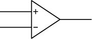
The input marked with “+” is known as the noninverting input, and the input marked with “-” is the inverting input. If the voltage present at the noninverting input is greater than that present at the inverting input, the output of the op amp is positive. Conversely, if the noninverting input is less than the inverting input, the output is negative. Typically, an op amp’s output will not go as low as its negative power supply, nor as high as its positive power supply, due to the limitations of the internal circuitry. An op amp whose output voltage range does span the difference between its positive and negative power supplies is said to have rail-to-rail operation .
In order to function correctly, an op amp requires feedback . Feedback involves coupling the output of an amplifier back to its input. Negative feedback uses the output to reduce the gain of the amplifier and, in doing so, improves the amplifier’s other characteristics, such as the flatness of the frequency response and immunity to distortion. Negative feedback is achieved simply by connecting a resistor between the output and the inverting input, as we will shortly see. (A circuit with no feedback is said to be open-loop.) Op amps are designed in such a way as to make the output change to cancel the difference between the inputs via a feedback resistor. Thus, the output waveform follows the difference between the input waveforms. The magnitude of the output is proportional to the feedback resistor. The larger the resistor, the more the feedback of the output is attenuated. Thus, the op amp makes the output larger to compensate. In this way, the output is an amplified version of the input.
An op amp may either be used as an inverting amplifier (Figure 13-3) or a noninverting amplifier (Figure 13-4). An inverting amplifier “flips” the signal in addition to amplifying it.

The gain of an inverting amplifier is given by:
Gain = - R2 / R1
Note the minus sign. That’s because this amplifier inverts the signal.
You are more likely to use a noninverting amplifier (Figure 13-4), which doesn’t flip the signal. These are commonly used in audio and sensor applications.
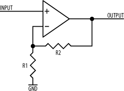
The gain of a noninverting amplifier is given by:
Gain = 1 + R2 / R1
The gain of the amplifier may be set under software control by using a digital potentiometer (Chapter 7) for R2.
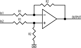
A differential amplifier (Figure 13-5) multiplies the difference between two input signals and is used to amplify small signals that may be subject to noise. By amplifying the difference between the signal of interest and a reference, any noise present is reduced (since the noise will affect both the signal and the reference equally). When both inputs to a differential amplifier change in the same way, this is known as a common-mode change. Ideally, a differential amplifier should be immune to common-mode changes, since its purpose is to amplify the signal difference. Its immunity to common-mode changes is known as its Common-Mode Rejection Ratio (CMRR ). The higher the CMRR, the better. To achieve a high CMRR, it is important to match the values (and tolerances) of the resistors as closely as possible.
The output voltage of this differential amplifier is given by:
VOUT = (In2 - In1) * (R2 / R1)
Analog to Digital Conversion
A device that converts an analog input voltage to a digital number is known as an Analog to Digital Converter, or simply and more commonly as an ADC. You may have also heard the term codec (COder DECoder) before. A codec is an ADC
combined with a Digital to Analog Converter ( DAC ), providing both analog input and analog output in one chip. We’ll look at DACs in more detail later in this chapter.
ADCs are found in cell phones and digital phones, converting your voice to digital data for transmission. They are also used in your computer to digitize the input from a microphone for speech recognition. Professional recording studios use ADCs to convert audio to digital data in preparation for CD mastering. Similarly, video is sampled using ADCs prior to DVD mastering. Your scanner, web cam, and digital camcorder all have ADCs in them. At the other end of the application spectrum, ADCs are used to sample inputs from sensors. These applications can range from automated weather stations to the system monitoring the processor temperature in your PC.
There are several different types of ADC. Integrating ADCs use an internal voltage-controlled oscillator to produce a clock signal whose frequency is proportional to the voltage being sampled. The clock signal is used to drive a counter, which provides the digital value for the sample. The higher the sampled voltage, the higher the clock frequency, and therefore the higher the number reached by the counter. The counter is reset prior to each conversion. Because of this conversion technique, integrating ADCs are not known for their speed of conversion.
A successive approximation ADC uses a DAC to provide an analog reference voltage that is compared to the input voltage. By incrementing the digital code driving the DAC, the reference voltage is increased until a match is found. Once this happens, the code used to drive the DAC is used as the digital output of the ADC.
Flash ADCs (also known as parallel ADCs) use a bank of comparators to compare the input voltage to a range of reference voltages. The conversion of the input analog voltage to a digital value is therefore very fast. The catch is that flash ADCs tend to be more expensive than other types of ADC and, due to their complexity, normally have a lower resolution than other forms of ADC.
The process of converting an analog signal to digital is known as sampling or quantization . ADCs have two principle characteristics: sample rate and resolution. Sample rate is expressed as samples per second (SPS) and refers to how frequently an analog input signal is converted into a digital code. The faster an ADC’s sample rate, the more expensive that chip will be. Resolution determines the accuracy of each sample. For example, an “8-bit ADC” will return an 8-bit code representing the sampled input signal. This means that the input has been quantized into one of 256 discrete values. An “11-bit ADC” will quantize the signal into one of 2,048 values, yielding a more accurate result. However, the higher the resolution, the more expensive the ADC. Further, high resolution is not always required. If, for example, you’re sampling a temperature sensor that has a range of 0ºC to 100ºC, with an accuracy of ± 0.5º C, then that sensor has only 200 meaningful voltage levels. For this sensor, an 8-bit ADC is fine. While you could use an 11-bit ADC to sample this sensor, the additional resolution is overkill.
An ADC will convert the analog signal into a number that represents the ratio of the input signal to a given reference voltage
. For example, if the ADC’s reference voltage is 5 V, and the input signal is 3 V, then the ratio of input to reference is 60%. So for an 8-bit ADC, where 255 represents full scale, the sampled input will be returned as 153 (0x99). From your point of view, you receive the value 153 from the ADC, and must work back from this to calculate the original analog voltage:
    Signal = (sample / max_value) * reference_voltage
           = (153 / 255) * 5
           = 3 Volts
Sample Rates
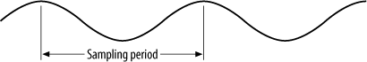
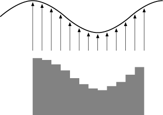
The rate at which a signal is sampled can have a dramatic effect on the quantized result and therefore can also affect the way in which software interprets that result. Figure 13-6 shows a sinusoidal signal that is sampled at a rate equal to its period. In this example, the sample happens to coincide with a peak in the signal. The signal changes in between samples, but our choice of sample rate means that we get the same value each time. We get a completely false picture of what is really happening to that signal. To our sampling software, each value returned is the same, and so the signal appears to us as though it were a flat line!
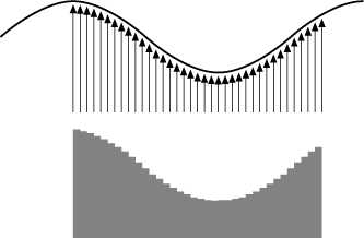
If we choose a sample rate that is double (or more) than the signal’s highest frequency component, we can see the signal in more detail (Figure 13-7). This sampling frequency is known as the Nyquist frequency and is the lower limit of what will produce usable results. If the sample rate is slower than the Nyquist frequency, false artifacts (such as our sine wave appearing as a straight line, as we saw previously) may appear in the sampled result. These phantoms are known as aliasing.

Tip
Ever see an old Western movie where the wheels of a wagon appear to be rotating backward, even though the wagon is moving forward? That’s an example of aliasing. The frame rate of the camera is effectively sampling the rotation of the wheels. Because the wheel rotation is slightly slower than the frame rate, the wheel doesn’t quite make a full revolution per frame. So on each successive frame, the wheel appears a little further behind than it was on the preceding frame. The effect is as though the wheel is rotating backwards—aliasing in action!
The faster the sample rate, the more accurate your sampled results will be. Since your sampling is quantizing the signal both in terms of amplitude (ADC resolution) and time (sample rate), a quantization error will always result (Figure 13-8).
As you can see, the smooth sine wave of the original signal has become a jagged representation. Now, if you were monitoring temperature, this might be sufficient. You might not care how the temperature signal changed. Instead, you might be interested in the temperature only at specific intervals, and with only a limited accuracy. In such a case, this effect is not really a problem.
However, if you were sampling audio, this quantization effect could be a real problem. By increasing the sample rate, a more accurate representation of the original signal is obtained (Figure 13-9).
A voice-mail system may use a sample rate of only 8 kHz and a resolution of 12 bits, and the resultant sound quality is limited. However, CD audio uses a sample rate of 44.1 kHz with 16-bit data and achieves a significant improvement in quality as a result. DVD audio uses a sample rate of 48 kHz with 24-bit data for even greater audio fidelity. To further improve sound quality, both CD and DVD players have special output filters to smooth the transitions between each sample when the data is converted back into analog form.
The take-home message is that you should choose your ADC resolution and sample rate carefully, keeping in mind exactly what you’re sampling and what you intend to use it for.
Interfacing an External ADC
There is a very wide range of ADCs available, for every considerable purpose. Choose from very low-cost, low-speed ADCs for simple voltage conversion to very high-speed, precise (and expensive) ADCs for sampling video streams. Many microcontrollers have inbuilt ADC subsystems, making analog interfacing simple. However, if the processor doesn’t incorporate an ADC, or its ADC is not suited to your application, it becomes necessary to add an external device.
A good general-purpose ADC for sensor applications is the Maxim MAX1245. It has eight channels of analog input and can sample at 100,000 samples per second, with a resolution of 12 bits. (There are similar devices with resolutions ranging from 8 bits to 16 bits, and with interfaces such as SPI, I2C, and processor bus.) The MAX1245 has an internal track and hold, preventing a changing signal from corrupting the result during a conversion. The MAX1245 is interfaced to a host processor via an interface that is compatible with SPI, Microwire, and the serial interfaces found in Texas Instruments TMS320-series DSP processors (Figure 13-10). As you can see, the MAX1245 is very easy to use. In this schematic, the analog input comes in via an IDC header, the 16-pin connector on the left of the figure. Note that every second pin on the connector is tied to ground. This means that every second wire in the connected cable will be grounded, providing a degree of noise immunity to our analog signals.

The DOUT, DI, and SCLK signals correspond to a processor’s SPI MISO, MOSI, and SCLK signals, respectively. ![]() is simply generated using a processor I/O line.
is simply generated using a processor I/O line.
A conversion commences by sending a start command to the ADC via the SPI interface. The start command is simply a byte that specifies the channel and other ADC settings for that particular conversion. (Refer to the MAX1245 datasheet for more information on the software interface.) The MAX1245 may use an internal clock source to drive the conversion process, or it may have an external clock. The SPI SCLK also doubles as the conversion clock, when the ADC is used in external-clock mode. When used in internal-clock mode, the output, SSTRB (Serial Strobe), goes low at the beginning of a conversion and returns high once the conversion is complete. When an external clock is used, SSTRB pulses high in the clock period prior to the most significant bit being processed. SSTRB may be used to flag the completion of a conversion to a host processor by acting as an interrupt input. Alternatively, when used in external clock mode, the conversion result is ready once the start command has been sent.
The MAX1245 has the ability to enter low-power mode. This can be done either through hardware or software control. The MAX1245 has an input pin, ![]() , which, when asserted low, places the ADC into low-power operation. Now, interestingly,
, which, when asserted low, places the ADC into low-power operation. Now, interestingly, ![]() is also used to specify the clock frequency of the ADC’s internal sampling. Sending this input high sets the clock to 1.5 MHz, whereas leaving the input to float (no connection) sets the clock to 225 kHz. If
is also used to specify the clock frequency of the ADC’s internal sampling. Sending this input high sets the clock to 1.5 MHz, whereas leaving the input to float (no connection) sets the clock to 225 kHz. If ![]() is driven by a microcontroller’s I/O pin, changing that pin’s configuration from an output to an input will effectively float
is driven by a microcontroller’s I/O pin, changing that pin’s configuration from an output to an input will effectively float ![]() . In this way, you can still use the “no connection” option even when the pin is connected. The MAX1245 can also be placed into low-power mode by software. If the two least significant bits of the start command are both 0, then the MAX1245 is placed into shutdown. The advantage of software power-down is that you can request a conversion and place the device into shutdown with a single command. The ADC will complete the conversion before shutting down, and its interface will remain active so that the result may be clocked out to the microcontroller.
. In this way, you can still use the “no connection” option even when the pin is connected. The MAX1245 can also be placed into low-power mode by software. If the two least significant bits of the start command are both 0, then the MAX1245 is placed into shutdown. The advantage of software power-down is that you can request a conversion and place the device into shutdown with a single command. The ADC will complete the conversion before shutting down, and its interface will remain active so that the result may be clocked out to the microcontroller.
Power for the MAX1245 (VDD) can be in the range of 2.7 V to 3.3 V. The MAX1245 has three ground pins: COM, DGND, and AGND. COM is the ground reference for the analog inputs, DGND is the ground connection for the digital section of the ADC, and AGND is the ground connection for the analog section of the ADC. These three grounds need to be connected together, but only at a single point, close to AGND. This is known as a star ground point . The two power inputs (VDD) need two decoupling capacitors to remove noise from the supply voltage. A 0.1 μF capacitor and a 4.7 μF capacitor should be used to decouple VDD and should be placed as close to the star ground point as possible. For particularly noisy power supplies, a 10 Ω resistor should be placed in series between the power source and VDD. The analog inputs should be shielded from all nearby digital signals to prevent interference, and a ground shield (a fill) should be placed under the MAX1245 to further isolate the device from noise. (See Chapter 6 for more information on noise and shielding.)
Now that we have seen how to add an ADC to a microcontroller, let’s give it something to sample. We’ll now take a look at some sensors and see how to interface them to an ADC. There are lots of different sensors available, from many manufacturers. Many are hard to use, awkward to interface, and require much more effort than seems necessary. But not all sensors are created equal. I have sought out and selected a range of sensors that are trivial to use and require little or no design effort. Electronics can be hard, but it doesn’t always have to be so, as you will see.
Temperature Sensor
We’ll start with something simple: a temperature sensor. This little sensor has a wide range of applications. The most obvious is as an environment monitor or weather station, but you could also use it to sense temperatures inside rooms and to control the appropriate heating or cooling systems. Combine it with a datalogger design, and you have a temperature recorder. Such devices are used in the shipment of fruits, vegetables, frozen foods, and flowers to ensure that they get to market in their best condition. It can also be used in the shipment of blood products and pathology samples, making sure that these critical substances are not exposed to adverse temperatures.
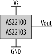
The AD22100 and AD22103 temperature sensors, by Analog Devices, are very easy to use. They are 3-pin devices,[*] requiring only power (V S) and ground to give you a voltage output that is proportional to temperature (Figure 13-11). The AD22100 requires a 5 V supply, and the AD22103 requires a 3.3 V supply.
What could be easier than that?
The output voltage corresponds to 22.5 mV/ºC over the temperature range -50ºC to +150ºC for the AD22100 and 28 mV/ºC over the temperature range 0ºC to 100ºC for the AD22103. The transfer functions (how the output relates to the input) for the two devices are given by:
    VOUT = (VS / 5) x [1.375 + (0.0225 x TA)]            AD22100
    VOUT = (VS / 3.3) x [0.25 + (0.028 x TA)]            AD22103
where V OUT is the output voltage, V S is the power supply, and TA is the ambient temperature.
So, turning the equations around, the relationship between temperature and output voltage is:
    TA = (((VOUT x 5) / VS) - 1.375) / 0.0225           AD22100
    TA = (((VOUT x 3.3) / VS) - 0.25) / 0.028           AD22103
For example, if we were using an AD22100 temperature sensor with a supply voltage of 5 V (V S = 5 V), then our function becomes simply:
TA = (VOUT - 1.375) / 0.0225
Thus, if we measured an output voltage of 1.94 V, the corresponding temperature would be 25.1ºC.
Interfacing the temperature sensor to an ADC is simple. The output may be directly connected to an input of the ADC. Alternatively, since temperature changes relatively slowly, we can add an RC filter between the sensor and the ADC to remove any noise that may be present in the output (Figure 13-12).

Light Sensor
Now we’ll take a look at a light sensor. The obvious use of a light sensor is to monitor natural light levels, and perhaps use the results to control artificial-lighting systems. But combine this sensor with a directional light source (such as a bright LED enclosed in a baffle), and you have a security detector. As long as the sensor can “see” the LED, everything’s fine. But when the light is interrupted, you know that someone or something has passed between.
Tip
I used the particular sensor we’re going to look at on a small datalogger. One of my customers is a biologist who studies albatrosses (giant seabirds) of the southern oceans as part of an ongoing conservation program. These birds will fly for years at a time, circumnavigating the world on the ocean winds. The tiny datalogger (smaller than your smallest finger) weighs only a few grams and is attached to the bird’s leg. (The attachment is designed and fitted with great care to ensure that the bird is not harmed or adversely affected in any way.) The light sensor is used to record sunlight levels that the bird experiences on its journey.
By comparing the recorded sunrises and sunsets with the reference clock aboard the datalogger, and looking at the duration of twilight, latitude and longitude can be computed. In this way, the simple recording of light levels is used to track an albatross’s journey as it circumnavigates the world.
The recorded light profiles also give information about what the albatross does. You can tell whether the bird was flying with feet tucked up in the feathers, flying with feet hanging down, or resting on the water, as each activity has a unique light profile associated with it. You can also see the phases of the moon leaving their trace on the nighttime light levels, as well as which days were cloudy and which were sunny. It even detects when the albatross stumbles across a lonely, and brightly lit, squid boat during the night. One simple sensor can tell you an awful lot. For more information, see http://www.oreillynet.com/pub/a/oreilly/cprog/news/albatross_1202.html.
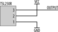
There are lots of commercial light sensors available. We’re going to take a look at the TAOS TSL250R sensor. TAOS (http://www.taosinc.com) is short for Texas Advanced Optical Solutions, Inc., a spin-off company from the venerable Texas Instruments, Inc. The TSL250R (Figure 13-13) consists of a photodiode (a semiconductor that is responsive to light) and an integrated amplifier. Like the temperature sensor we’ve just seen, the TSL250R just needs power and ground, and it will give you an analog voltage output that is proportional to incident light.
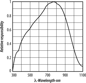
The spectral response for the TSL250R, shown in Figure 13-14, ranges from ultraviolet (left) to infrared (right) and peaks in the visible part of the spectrum.
The TSL250R can operate from a supply voltage of between 2.7 V and 5.5 V and typically consumes only 1.1 mA of current. The basic circuit for the TSL250R is very simple (Figure 13-15).
The maximum output voltage (under full irradiance) for this sensor is just under 4 V, when the part is powered from a 5 V supply. So, if we choose, we can interface this sensor directly to a (5 V referenced) ADC without any additional amplification. Now, because the output does not span the full scale of the ADC’s range, we lose a small amount of resolution. For an 8-bit ADC, a 4 V input corresponds to 0xCC, and so our range of values for this sensor go from 0x00 to 0xCC. Depending on your application, this may not be a problem. For example, if you are interested only in detecting the difference between light and darkness, or when a given low-light threshold is crossed, this will work fine.
Amplifying the Light Sensor
If you do want to sample the full range of the sensor, you need to amplify the sensor’s output. Since the sensor’s maximum output is 4 V and the reference of the ADC is 5 V, the gain of the amplifier must be 1.25.
A good general-purpose op amp is the AD623 by Analog Devices. It has rail-to-rail operation, can run from a single supply voltage, requires very little current, and is exceptionally easy to use. Analog Devices has done a lot of the hard work already, and the AD623 requires only a single external resistor to set the gain. The value of the resistor is calculated using the relation:
RG = 100 kΩ / (Gain - 1)
So, for our required gain of 1.25, we need a resistance of:
    RG = 100 kΩ / (1.25 - 1)
       = 100 kΩ / 0.25
       = 4 kΩ
The resistor should have a tolerance (accuracy) of 1% or better. Standard off-the-shelf resistors are normally 5% and just aren’t accurate enough.
The circuit with the TSL250R interfaced to the AD623 is shown in Figure 13-16.
The output of the TSL250R sensor (pin 3) is connected to the noninverting input of the AD623 op amp (pin 3), while the inverting input is tied to ground. The gain resistor is connected between pins 1 and 8. The negative power supply, -VS, is connected to ground for single-supply operation. The positive power supply, +VS, is

connected to VCC and is decoupled to ground using two capacitors. The op amp’s reference input (REF) is also tied to ground. The output of the op amp at pin 6 is then connected directly to the analog input of an ADC.
Accelerometer
Now we’re going to take a look at an interesting sensor. Analog Devices makes some really nice accelerometers, and we’ll learn how to interface an ADXL150 to an embedded system. You can use an accelerometer for a number of applications, not just for measuring linear acceleration of vehicles. The ADXL150 is a single-axis (one- dimensional) accelerometer with a resolution of 10 m g and a full-scale range of ±50 g. For dual-axis (two-dimensional) sensing, choose the ADXL250.
Tip
g is the unit of acceleration. One g is approximately equal to 9.8 m/sec2 (32.2 feet/sec2). As a passenger in a commercial jet aircraft, you’ll experience a force of about 2 g when the aircraft turns. A fighter aircraft will experience a force of around 8 g when turning sharply. Without a special suit, the jet fighter pilot would black out under a force of 8 g. So the ADXL150, with a range of ± 50 g, can measure a significant amount of force!
Such a fine resolution means you can use this sensor to measure gentle vibrations and shifts. You could use it in a seismometer for geophysical applications or to measure vibrations or ground shift in mines, tunnels, or at building sites. You could use it to monitor motion and, by placing three accelerometers orthogonally, get an accurate 3-D motion recorder. The same setup could also be used as a digital carpenter’s spirit level by sensing the direction of the Earth’s gravitational field. Perhaps you might use it to monitor violent physical shock, such as crash-test measurements. Ever moved to a new house only to discover that Granny’s fine crystal glassware was smashed by the movers? Place one of these (along with an appropriate small datalogger) into the packing boxes, and you’ll be able to prove just how rough the gorillas from the moving company were. As you can see, this chip has lots of applications.
The axis of sensitivity for the ADXL150 runs along the chip’s length from top to bottom (Figure 13-17). It is important when using this device that it be securely mounted to the circuit board. Rather than just relying on solder, also use strong glue under the chip to bind it to the circuit board.

The ADXL150 requires no external components (save for power-supply decoupling) and is a completely self-contained unit, incorporating not only the sensor, but also signal conditioning and amplification. Its output can be interfaced directly to an ADC. The schematic for using the ADXL150 is shown in Figure 13-18.

Most of the pins are No Connection (NC) and can be ignored, as can the TESTPOINT and SELF-TEST pins. The TESTPOINT pin is used during manufacture only and should be left alone.
The ADXL150 operates off a power supply in the range of 4 V to 6 V. However, for ideal operation, the supply should be exactly 5.0 V. The closer to 5 V the supply is, the more accurate your measurements of acceleration will be. The output voltage is proportional to both acceleration and power supply (VS) and is given by the relation:
VOUT = VS/2 - (sensitivity * VS/5 * acceleration)
The sensitivity value varies from device to device and is in the range 33.0 to 43.0, with a nominal value of 38.0. The standard sensitivity value gives a range of ± 50 g; however, the sensitivity may be doubled (giving a range of ± 25 g) by connecting the output to the OFFSET-NULL pin.
The SELF-TEST pin is used for verifying the correct operation of both the internal mechanics of the sensor, as well as its signal conditioning and amplification electronics. Applying a logic 1 to this input pin artificially imposes a force on the sensor, and thus the sensor can be shown to be operating correctly.
Pressure Sensors
Now let’s take a look at pressure sensors. The most obvious use of these sensors is in measuring air pressure for weather monitoring and prediction. But pressure sensors are also used in cars to measure manifold pressure, in washing machines to measure water levels, and in biomedical applications such as measuring blood pressure. Another application of pressure sensors is to measure altitude, since air pressure changes with height above sea level. Ocean depth can similarly be measured.
When using pressure sensors, the substance you are measuring can adversely affect the device. Remember that these are sensitive electronic components, and fluids or corrosive gases can destroy them. So unless you’re measuring clean, dry air, you’ll need to provide some degree of environmental protection for your sensor. Just how you do that really depends on what the application is, what environmental conditions you must protect against, and how far your budget stretches.
Pressure sensors work by measuring the deflection of a diaphragm separating two chambers. One chamber is exposed to the pressure that is being measured, while the other chamber holds a reference pressure. The pressure difference between the two chambers causes the diaphragm to deflect, and this deflection is converted into a voltage that is proportional to the pressure difference. Pressure sensors come in three types: absolute , differential , and gauge .
In an absolute pressure sensor, the reference chamber is sealed. Pressure readings are referenced to an absolute pressure, hence the name. Absolute sensors normally have the reference chamber pressure at vacuum, or at 1 atmosphere.
In a differential sensor, the reference chamber is not sealed, and an external pressure reference may be applied. Differential sensors are used to measure the relative pressures between two gases or two liquids. A differential sensor may be treated as an absolute sensor by providing it with a sealed and stable reference pressure.
A gauge sensor is a variation of the differential pressure sensor, where the reference pressure chamber is open to the atmosphere. Thus, the measured pressure is referenced to atmospheric pressure, and variations of atmospheric pressure (such as those caused by weather conditions or altitude) are taken into account. One interesting use of a gauge pressure sensor is to measure airspeed. If the measuring chamber is exposed to the oncoming airflow (caused by the aircraft’s motion), and the reference chamber is exposed to the air but sheltered from the effects of the airflow, then the difference in pressure can be used to calculate the airspeed of the aircraft.
So, with all that in mind, let’s take a look at some pressure sensors. The first sensor is a Freescale (formerly Motorola) MPXA6115A absolute pressure sensor (Figure 13-19). It operates from a 5 V supply and will give an output voltage of between 0.2 V and 4.8 V, proportional to pressures of 15 kPa to 115 kPa. (Pa is short for Pascals, which is a unit of pressure.) Unlike most other pressure sensors, which require external signal conditioning, temperature compensation, and signal amplification, the MPXA6115A integrates it all in one neat little package. It comes in an 8-pin chip package, with or without snorkel!

The NC pins are no-connection and should be left unwired. The only additional components required are a decoupling capacitor on the power supply and a resistor and capacitor in parallel at the output. The output may be directly connected to an ADC’s input.
The second pressure sensor we will look at is also an absolute pressure sensor. But, unusually, rather than producing an analog output, it incorporates an inbuilt ADC. It is interfaced to a microcontroller using SPI and, being digital, it is much less susceptible to noise and interference. The sensor is the KP100, made by Infineon Technologies (http://www.infineon.com) in Munich, Germany.
The schematic for a circuit based on the KP100 is shown in Figure 13-20.
The sensor operates off a 5 V supply, and this is decoupled to ground using a 100 nF capacitor to reduce noise. The sensor has a standard SPI-style interface and is connected to a microcontroller, as with any SPI device. The sensor also provides a READY output, which may be used to interrupt the host processor, or may simply be connected to a spare I/O and read as a digital status flag. The KP100 also requires a separate clock (CLK) input. This clock can be either 4 MHz or 8 MHz. If the processor is running at one of these speeds, then the sensor can share the same clock input as the processor. However, if the processor is operating at a different clock frequency,

the KP100’s clock may be easily generated using a clock module. These 4-pin devices are available in a variety of standard frequencies and require only power and ground to generate a clock output.
Magnetic-Field Sensor
The final sensor we’ll look at is the AD22151 magnetic-field sensor by Analog Devices. Its primary use is for position and proximity sensing. A magnetic source is used as a reference point, and the sensor’s distance from that source may be easily determined by the measured field strength. The sensor has inbuilt temperature compensation and amplification.
The circuit for this sensor is shown in Figure 13-21. It’s a little bit more complicated than the other sensors we’ve looked at so far.
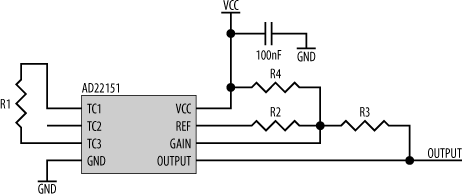
The sensor operates off a 5 V supply, decoupled to ground using a 100 nF capacitor. There are four resistors required for correct operation. R1 is the temperature compensation resistor, which should be connected between pins 1 and 3, or pins 2 and 3, depending on the applied magnetic field. For large external fields, R1 connects pins 1 and 3, as shown in Figure 13-21. For smaller fields, connect R1 between pins 2 and 3. The AD22151 datasheet has plots of values for R1 versus required compensation levels. Check with the manufacturer of your magnetic source[*] as to the required compensation value, and use this in conjunction with the datasheet to determine R1.
For magnet data, try http://www.magtech.com.hk, http://www.eastindustries.net, or http://www.millennium.com.hk as places to start.
R2 and R3 set the signal gain of the internal amplifier, and R4 provides a voltage offset. The datasheet for the sensor contains equations and technical data for computing values of these resistors, based on your specific needs.
The output of the sensor circuit may be connected directly to an ADC input for sampling.
Digital to Analog Conversion
So far, we have looked at how you can sense real-world effects and convert these into digital data. Now let’s see how to do the reverse: take digital data and convert it into an analog signal by using a chip known as a Digital-Analog Converter (DAC). We’ll also look at how you can produce an analog output using nothing more than a single digital I/O line.
All DACs have a digital input (a microprocessor bus, SPI, or I2C) and will provide you with one or more channels of analog output.
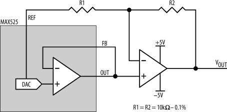
The Maxim MAX525 is an 11-bit DAC that interfaces to a host processor using SPI. It has four channels of analog output and incorporates output amplifiers on-chip. The inverting input of each amplifier is accessible so that you can alter their respective gains. A sample circuit for a MAX525 is shown in Figure 13-22.
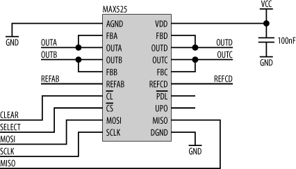
The four analog output channels are OUTA, OUTB, OUTC, and OUTD. These are tied directly to their respective feedback inputs (FBA, FBB, FBC, and FBD) for standard unipolar operation. There are two voltage reference inputs, REFAB (for channel A and channel B) and REFCD (for channels C and D). These two reference inputs must be at least 1.4 V or more below VCC at all times. The output voltage for each channel is given by the relation:
VOUT = (VREF * code / 4096) * gainwhere code is the digital value written to that channel. In our sample circuit, the gain is 1. (See "Amplifiers,” earlier in this chapter, for an explanation of how to set gains.) If our reference voltage is set to 3.6 V, the digital value 4095 (0xFFF) generates an output voltage of:
VOUT = (VREF * 4095 / 4096) * gain
        =  3.6 * 0.9997 * 1
        = 3.59 V
Similarly, the digital value 2048 (0x800) generates an output voltage of:
VOUT = (VREF * 2048 / 4096) * gain
        = 3.6 * 0.5 * 1
        = 1.8 V
Note the separate analog and digital grounds in the schematic. These should be connected together, but only at a single point close to the DAC.
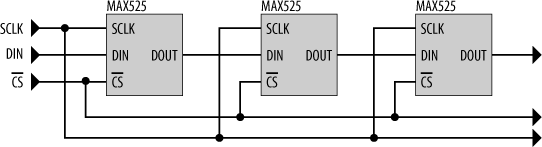
The MAX525 has a standard SPI connection to a microprocessor. Multiple MAX525s may be daisy-chained together for efficiency (Figure 13-23).
The MAX525 also has a ![]() input, which, when driven low by an I/O line, sends all outputs to their lowest value. The MAX525 can be put into low-power mode under software control. The input
input, which, when driven low by an I/O line, sends all outputs to their lowest value. The MAX525 can be put into low-power mode under software control. The input ![]() is Power-Down Lockout, and when driven low, it prevents the MAX525 from being shut down. This is important if the outputs are being used to drive a critical circuit or system. You don’t want the controlling voltages disappearing by accident. Finally, the good people at Maxim have provided a signal called UPO (User Programmable Output). This is a general-purpose output that can be driven high or low under software control. Use it for whatever purpose you require.
is Power-Down Lockout, and when driven low, it prevents the MAX525 from being shut down. This is important if the outputs are being used to drive a critical circuit or system. You don’t want the controlling voltages disappearing by accident. Finally, the good people at Maxim have provided a signal called UPO (User Programmable Output). This is a general-purpose output that can be driven high or low under software control. Use it for whatever purpose you require.
Now, if you wanted a gain other than 1 (non-unity gain), external resistors are required for the output amplifier. The schematic for this (for a single output channel) is shown in Figure 13-24.

From before, we know that the gain of a noninverting amplifier is given by:
Gain = 1 + R2 / R1
For bipolar output on a given channel, an external amplifier (with bipolar supplies) does the job (Figure 13-25).
PWM
Using a DAC may seem the obvious way to generate an analog output voltage, but there is another way that uses nothing more than a digital I/O line configured as an output. This technique is known as Pulse Width Modulation (PWM).
Consider the average, garden-variety, square wave shown in Figure 13-26.
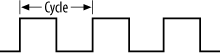
The width of the high is equal to the width of the low, so this wave is said to have a 50% duty cycle. In other words, it is high for exactly half the cycle. Now, if the amplitude of this square wave is 5 V, for example, the average voltage over the cycle is 2.5 V. It is as though we had a constant voltage of 2.5 V.
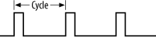
Now consider the square wave in Figure 13-27.

This wave has a 10% duty cycle, which means that the average voltage over the cycle is 0.5 V.
A low-pass (averaging) filter on the PWM output will convert the pulses to an analog voltage, proportional to the duty cycle of the PWM signal. By varying the duty cycle, we can vary the analog voltage. Hey, presto! We have digital-to-analog conversion without a DAC. That’s the basic idea behind PWM.
Tip
PWM can also be used to drive a LED, and thereby get varying light intensities from a signal that is essentially either on or off. PWM can also be used to generate audio. Early desktop computers, such as the Apple ][, used PWM to drive a speaker. Steve Wozniak, the designer of the Apple ][, used a spare chip select of the address decoder as his PWM signal. By changing how frequently a particular address was accessed, he was able to change the frequency and duty cycle of his PWM signal and was therefore able to generate simple audio with varying volume and pitch. Sound out of an address decoder!
Motor Control
One of the fun things you can do with an embedded computer is get it to actually move something, whether it be an external system or the embedded computer itself. Motion implies motor, and this section will look at how you interface an embedded computer to an electric motor. The possible applications could range from controlling locomotives on your model railroad layout to experiments in robotics, and anything in between. A note of caution, though: if your hardware and software are responsible for moving a physical object, then a bug can easily cause physical damage too. So be careful.
Let’s say that we have an electric motor than operates from a 12 V supply. Applying 12 V across the motor will cause it to turn at full speed. Similarly, by applying 6 V, we can get the motor spinning at half speed. By varying the applied voltage, we can vary the speed at which the motor turns.
There are several ways to generate this voltage to drive the electric motor. The most obvious may seem to be to use a DAC to generate an analog output voltage and then use an amplifier to boost the signal to the voltage and current required to turn the motor. The speed of the motor is proportional to the output voltage. However, this technique has a major drawback. For very low-speed operation, the required output voltage may be too low to actually cause the motor to turn.
A better way is to use PWM. Consider the PWM signal in Figure 13-28, with an amplitude of 12 V.
With a 10% duty cycle, the effective analog output voltage of this PWM signal is 1.2 V. Now, by itself, 1.2 V may not be enough to turn a motor. But we’re not using 1.2 V; we’re actually pulsing the motor with 12 V, its maximum drive voltage. The duration of the pulses gives the equivalent speed of a motor voltage of 1.2 V. However, by using a full 12 V amplitude, we’re ensuring that the motor will turn. This is the advantage of PWM. To control speed, we vary the width of the pulse and not the amplitude.
Using PWM, you can get very slow motor speeds and very fine control. The pulses can cause a jerkiness to the motor if the overall frequency is low, but by choosing a high frequency, the jerkiness is averaged out.
Many microcontrollers have internal, software-programmable PWM modules that make generating PWM signals easy. Even if a processor does not have a PWM module, you can still generate PWM under software control simply by using a digital output line.
Let’s now take a look at how you would interface a processor to an electric motor using PWM. Due to the voltages and currents required by motors, you cannot simply hang a motor off the pins of a processor and expect it to work. You need an interface circuit that will take your logic-level, PWM output and use this to switch much higher voltages and currents.
Figure 13-29 shows a conceptual model (in a crude and simplified form) of such an interface circuit for driving a small electric motor. This type of circuit is known as an H-bridge.

It’s not as confusing as it first looks. Don’t be too worried about the transistors (Q1-Q4) in the circuit. They simply act as switches. Our motor operates from a supply voltage, V+. Apply V+ with one polarity, and the motor turns in the forward direction. Reverse the polarity, and the motor reverses too. To drive the circuit, we use four outputs from the processor: two PWMs (which I’ve called PWM-A and PWM-B) and two general I/O lines (which I’ve called A and B). Initially, all outputs are low, everything is turned off, and the motor is stationary.
If we send A high, the transistor Q4 turns on and connects the right “side” of the motor to ground. If we then send PWM-A high, the transistor Q1 turns on. Thus, the left “side” of the motor is connected to V+, and the motor spins. By generating a PWM signal on PWM-A, we can control the speed of the motor in that direction.
Conversely, by leaving A and PWM-A low and setting B and PWM-B high, transistors Q2 and Q3 turn on, and the motor spins in the reverse direction. By generating a PWM signal on PWM-B, we can control the speed in the reverse direction.
Care must be taken in your software. If both Q1 and Q3 are turned on, or both Q2 and Q4 are turned on, then you effectively connect V+ to ground, with very little resistance in between! The results would be spectacular and short-lived! A proper H-bridge circuit normally contains protection to prevent such a state from occurring.
The actual implementation of an H-bridge is a little more complicated and requires additional components such as protection diodes and so forth. Now, while you could design such an H-bridge circuit using discrete components, there is an easier way. A number of manufacturers—such as Freescale, International Rectifier (http://www.irf.com), M. S. Kennedy Corp (http://www.mskennedy.com), and others—make H-bridges in easy-to-use integrated circuits.
Tip
If you’re ever cruising around a component manufacturer’s web site looking for devices that will switch high currents at high voltages and you can’t find them, scoot over to its “automotive components” section. Such devices are sometimes hidden away in there.
Let’s look at a sample H-bridge, the Freescale MC33186 . This chip is more sophisticated than the simple H-bridge used to explain the concept. It provides more functionality, yet is easier to control. This chip can operate from a supply voltage (V+) of between 5 V and 28 V and can switch continuous currents as high as 5 A, yet it has logic inputs that are compatible with TTL levels. It has inbuilt short-circuit and over-current protection. Figure 13-30 shows an MC33186 circuit.

The chip has three power-supply inputs, V BAT, all of which must be connected to the supply voltage, V+. The power-supply input needs to be decoupled using a 47 μF capacitor. The internal charge pump also needs a decoupling capacitor. The pin, CP, provides access to the charge pump and is connected to a 33 nF capacitor. The chip also has five ground pins, which, similarly, must all be connected to ground.
OUT1 and OUT2 are the pins that directly drive the motor. There are two of each, so that the high output currents are not traveling through a single pin.
IN1 and IN2 control both the motor’s speed and direction. DI1 and DI2 serve to disable the MC33186. These four control signals may be driven by a microcontroller’s I/O lines. For normal operation, DI1 is low and DI2 is high. Sending either DI1 high or DI2 low will disable the MC33186 and stop the motor. Table 13-1 shows how IN1, IN2, DI1, and DI2 affect the motor’s operation.
|
DI1 |
DI2 |
IN1 |
IN2 |
OUT1 |
OUT2 |
Motor |
|
Low |
High |
High |
Low |
V+ |
Ground |
Forward |
|
Low |
High |
Low |
High |
Ground |
V+ |
Reverse |
|
Low |
High |
Low |
Low |
Ground |
Ground |
Free-wheeling |
|
Low |
High |
High |
High |
V+ |
V+ |
Free-wheeling |
|
High |
Don’t care |
Don’t care |
Don’t care |
High impedance |
High impedance |
Disabled |
|
Don’t care |
Low |
Don’t care |
Don’t care |
High impedance |
High impedance |
Disabled |
If we want the motor to run forward, we generate a PWM signal on IN1 and leave IN2 low. If we want to run the motor backward, we leave IN1 low and place a PWM signal on IN2. The duty cycle of the PWM signal determines the motor’s speed. Simple.
If IN1 and IN2 are in the same state, then there’s no voltage difference applied across the motor’s terminals, and so the motor is not driven.
Pin 2 of the MC33186, SF, is an output status flag. If the MC33186 is operating correctly, SF is high. If there is a fault, SF is driven low. SF may therefore be used as an interrupt to alert the host processor of a problem.
The input COD determines how the chip functions during a fault. If COD is left unconnected or is connected to ground, a change on either input DI1 or DI2 will reset the fault condition. If COD is connected to VCC (that’s +5 V, not necessarily V+), then DI1 and DI2 are disabled. The fault condition can be reset only by a change on IN1 or IN2.
Using an integrated H-bridge circuit, such as the MC33186, greatly simplifies interfacing your embedded system to motors.
Sensing Motor Speed
In a control application, it is very useful to be able to sense a motor’s speed. The physical system (load) that the motor is driving will affect the motor’s rotation. If the motor must move a heavy load, then its actual speed of rotation may be less than the intended speed. In such situations, it is useful to measure the actual speed so that the embedded control system can compensate.
The easiest way to measure a motor’s rotational speed is to use an optical encoder module, such as the Agilent HEDS-9000 or a similar device. The encoder consists of a light source (LED) and an array of photo-detectors, separated from each other by a slotted disc known as a code wheel(Figure 13-31). The disc is mounted on the rotating motor shaft. Each time a slot passes between the LED and a detector, the detector receives a flash of light and generates an electrical pulse. The rate at which the pulses are generated corresponds directly to the rotational speed of the motor. The resolution of the code wheel is known as its counts per revolution (CPR) value. The HEDS series of encoders are available with CPRs ranging from 96 all the way up to 2,048.
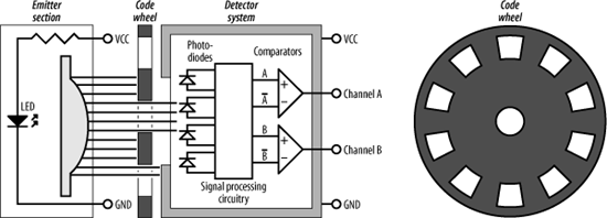
The HEDS-9000 optical encoder operates from a 5 V supply and has two outputs, A and B. These outputs are derived from two adjacent optical sensors. If the code wheel is rotating in one direction, output A will trigger before output B (Figure 13-32).

If the wheel is rotating in the opposite direction, then B will trigger before A (Figure 13-33).
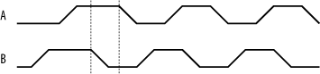
The rate at which the pulses arrive gives the motor’s speed, and the order in which they arrive shows the direction. This is known as quadrature encoding .
Most microcontrollers have timer/counter inputs that can measure external trigger events such as these. Under software control, you can use the timers to monitor these quadrature signals. However, Agilent makes a series of devices known as quadrature counters: the 11-bit HCTL-2000, the 16-bit HCTL-2016, and the 16-bit, cascadable HCTL-2020. These chips provide a bus-based interface to a processor and convert quadrature signals into a binary number representing motor position. A 16-bit position counter is capable of measuring 32,767 increments in either direction, which corresponds to approximately 15 turns of a 2,048 CPR encoder. To determine the present motor speed or position, the processor simply reads from the quadrature counter as though it were just another memory location. Quadrature counters also have noise filters on their inputs and so provide a more reliable and accurate way of determining motor position.
The schematics showing an optical encoder and quadrature counter are shown in Figures 13-34 and 13-35, respectively. The optical encoder is placed on a separate, small PCB so that it may be easily mounted next to the motor’s shaft. The quadrature counter is located on the embedded computer’s PCB. IDC headers (J1 and J2) and a ribbon cable connect the two circuit boards.


The quadrature counter requires a 14 MHz clock. This is easily provided by an oscillator module. CHA and CHB are the quadrature inputs from the encoder. The counter has a reset input, ![]() , which clears the counter. Asserting
, which clears the counter. Asserting ![]() zeros the quadrature counter and indicates that the motor is in the “home” position. This input is driven by a digital output of the microcontroller so that the counter can be reset under software control.
zeros the quadrature counter and indicates that the motor is in the “home” position. This input is driven by a digital output of the microcontroller so that the counter can be reset under software control.
D0 to D7 are the data buses through which the processor reads the current position. Since the counters are either 12 bits or 16 bits, two reads are necessary to retrieve the value through the 8-bit bus. The counter therefore occupies two locations in memory, and the SEL input is used to select which byte is being read. If SEL is low, then the higher-order bits are read. If SEL is high, then the lower-order bits are read. To make these two bytes appear in adjacent memory locations, the processor’s address line, A0, is used to drive SEL. Thus, the least significant address of the two selects the upper eight bits, while the next address selects the lower eight bits.
Now, the counter does not have a chip select as such. Since it is a read-only device, the counter’s output enable, ![]() , functions as a combined chip select and output enable. Therefore, this input is driven by the output of the address decoder that corresponds to the region of the address space to which the counter is mapped. When the processor reads from that address range,
, functions as a combined chip select and output enable. Therefore, this input is driven by the output of the address decoder that corresponds to the region of the address space to which the counter is mapped. When the processor reads from that address range, ![]() is asserted and the counter responds with data. Note that if the processor attempted to write to the counter, the counter would be selected and would respond with data. Therefore, both the processor and the counter would be attempting to drive data onto the data bus. This could potentially damage both chips. Now, with careful coding this would not be a problem. However, a crashing program may inadvertently cause this situation to arise. To prevent this, a better solution is to include the processor’s read strobe as part of the address decode for this particular device. In other words, the counter is selected if (and only if) both the address is correct and the processor is performing a read. If the processor is performing a write to the counter’s address, the counter is not selected and the access is ignored.
is asserted and the counter responds with data. Note that if the processor attempted to write to the counter, the counter would be selected and would respond with data. Therefore, both the processor and the counter would be attempting to drive data onto the data bus. This could potentially damage both chips. Now, with careful coding this would not be a problem. However, a crashing program may inadvertently cause this situation to arise. To prevent this, a better solution is to include the processor’s read strobe as part of the address decode for this particular device. In other words, the counter is selected if (and only if) both the address is correct and the processor is performing a read. If the processor is performing a write to the counter’s address, the counter is not selected and the access is ignored.
Switching Big Loads
We’ve already seen how to use an H-bridge chip to switch relatively large voltages (and the corresponding big currents) needed to drive electric motors. There are many other cases where you want to turn large voltages on or off, and, in this section, you’ll learn an easy way of doing just that.
The Freescale MC33298 is a chip that is controlled by a microprocessor using SPI that can switch eight power sources on or off. This chip can handle voltages between 5 V and 26.5 V, with currents as large as 6 Amps. If you need to turn electrical systems on or off, this chip is for you. Its primary use is for industrial and automotive applications, controlling power to subsystems such as heaters, small air-conditioning units, moderate-voltage light bulbs, small pumps, and so on. Obviously, it won’t handle the high AC voltages that come out of your wall socket, so don’t use it for switching power to your home appliances!
The basic schematic for the circuit is shown in Figure 13-36.

The MC33298 has two power-supply pins. VDD is a 5 V supply and powers the chip’s internal digital logic. It’s decoupled to ground using a 100 nF capacitor. V PWR is the supply voltage for the external subsystems (represented in the figure by each “LOAD” rectangle) and can range from 5 V to 26.5 V. There are eight switch outputs, labeled OUT0 through OUT7. When a given switch is activated, the corresponding output is connected to the V PWR supply, thereby turning on that subsystem. The MC33298 has short-circuit detection and shutdown (with automatic retry), over-voltage detection and shutdown, current limiting on the outputs, output clamping during inductive switching, and thermal shutdown if the device is dissipating too much power. Higher currents may be switched by tying two or more outputs together so that the current is shared by more than one pin. By tying all outputs together, currents as high as 48 A may be switched, limited only by the total power dissipation and corresponding thermal shutdown limit.
The chip has a standard SPI port, allowing it to be interfaced to, and therefore controlled by, most microprocessors. The SPI signals MOSI, MISO, and SCLK are connected directly to a processor’s SPI pins. The chip’s select input, ![]() , is controlled by a digital output of the processor and is used to select the device during a SPI transfer. The device may be reset and all outputs turned off by asserting its
, is controlled by a digital output of the processor and is used to select the device during a SPI transfer. The device may be reset and all outputs turned off by asserting its ![]() input. Again, this too can be driven by a digital output of the processor so that the chip may be turned off under software control. The MC33298 supports SPI daisy chaining, so multiple devices may be coupled together.
input. Again, this too can be driven by a digital output of the processor so that the chip may be turned off under software control. The MC33298 supports SPI daisy chaining, so multiple devices may be coupled together.
The SPFD pin is Short Fault Protect Disable. Sending this pin high allows the internal over-current detection circuitry to be disabled. When switching some loads, such as light bulbs, there is a very high current for a short period of time. This would normally cause the MC33298 to register an over-current fault and shut off that output. The SPFD pin allows this protection to be overridden so that such loads may be controlled. Even though the over-current protection is bypassed, the MC33298 is still protected. If the high current lasts long enough, the chip’s thermal shutdown circuit will kick in, thereby preventing damage. SPFD may be driven by a processor digital output, and should be used with caution! For normal operation (with over-current protection on), this pin should be low.
Now we’ve finished looking at I/O options for our embedded computers. In the next chapter, we’ll look at some processors and see how to design complete embedded systems.
[*] In some special applications, amplifiers may still be constructed using discrete transistors (or even valves).
[*] These devices are also available in 8-pin surface-mount chips, where five of the pins are unconnected.
[*] I’m assuming here that you are using a magnet specifically intended for such applications, and which has data available, rather than a magnet you’ve found lying around somewhere.