
Chapter 18. 68000-Series Computers
All is flux, nothing stays still.
—Heraclitus, Diogenes Laertius’ Lives of Eminent Philosophers
In this chapter, we’ll take a look at a 32-bit processor that has been around for quite some time and has evolved into a plethora of controllers and embedded processors. The 68000 (also known as the “68k”) is produced by Freescale Semiconductor and is licensed by several other manufacturers. The range of 68000-based processors is large (check out the manufacturers’ web sites for a list of processors and their features). The number of applications that the 68000 has found its way into is enormous. You can even get 68000s as soft cores for FPGAs, which means you place a 68000 CPU in the midst of your programmable logic, all on the one chip.
The Motorola[*] MC68000 was introduced in 1979 as the successor to its 8-bit 6800 family. It featured a large address space, 32-bit registers, a large number of addressing modes, and an enlarged instruction set with over 1,000 opcodes. It was designed with the intention of running multitasking operating systems, specifically Unix. Its use in Unix machines has now long since passed, having been usurped by more advanced RISC processors. The 68000 processor was also used in the original Macintosh computers, as well as in the Atari ST, the Commodore Amiga, and Jef Raskin’s CAT computer, all long extinct.
Tip
For an interesting overview of the CAT, read Jef Raskin’s The Humane Interface (Addison-Wesley Professional). He discusses the CAT’s unique design and has some interesting ideas on user interface design.
The processor’s wide range of software and reasonable computing power are now encouraging its extensive use in embedded systems. It now forms the basis of a family of microcontrollers designed for embedded systems, industrial control, networking, and PDAs. The 683xx series is the primary family of microcontrollers, specifically tailored to embedded applications. These processors combine a CPU32 core (68020-based) with various integrated functions (such as UARTs, SPI, ADCs, etc.). Additional 68000 processors have been developed for specialized applications. The original Palm PDA has a 68EZ328 DragonBall processor, also based on a CPU32 core, that incorporates an LCD controller along with many of the common functions found in PDAs. The DragonBall is essentially a PDA on a chip—just add memory. The ucLinux fraternity uses a DragonBall processor in its small embedded controller board.
The 68000 architecture was upgraded to RISC with the ColdFire series of processors. These see extensive use in industrial control and network interfaces.
The 68000 series of processors are good general-purpose processors. They have a nice instruction set, are easy (and fun) to write code for, and are relatively easy to build computers around. They have large address spaces and asynchronous operation, allowing them to be interfaced to a wide variety of memory and peripherals of varying operating speeds. They are used in industrial control and monitoring, and also in consumer electronics.
In this chapter, we’ll look at the standard 68000 processor. More than likely, this is not the processor you will use in a design. Rather, you will choose a 68000-based integrated controller that better suits your needs. So, why look at a standard 68000 and not one of the derivatives? First, there are far too many diverse 68000-based processors to cover. Second, since these processors are all based on the 68000, understanding the basic 68000 is a great starting point. Finally, all the derivatives are generally easier to use than the original, so if you can design around a standard 68000, then you can design for a derivative processor as well.
Understanding the 68000 gives you access to a wide range of available processors. There are dozens of commercial C compilers and assemblers available for the 68000 family, as well as a number of public-domain compilers as well. The 68000 is fully supported by the gnu development suite. Both Linux and BSD are also available for the 68000, as well as for numerous commercial operating systems.
The 68000 Architecture
The 68000 has eight 32-bit data registers (D0-D7), eight 32-bit address registers (A0-A7), a 32-bit program counter, two 32-bit stack pointers, and a 16-bit status register (Figure 18-1). The processor is capable of handling data as 32-bit long words, 16-bit words, bytes, or bits.
The processor has two modes of operation: supervisor mode (operating system) and user mode (applications). The mode of operation is made available to external

hardware, thereby giving the address decoder the ability to have separate supervisor and user spaces.
The standard 68000 is just a conventional, bus-based processor. A block diagram of a generic 68000-series processor is shown in Figure 18-2. The figure also shows the pins for a sample 68000-series processor. The pins and signals of 68000s can vary from one device to another, but they all have the same core functionality. The embedded controllers add to this basic functionality with additional I/O capability. We’ll look at the pins for the MC68EC000 shortly. You can download datasheets, programmers’ manuals, and technical references for 68000-series processors from the Freescale Semiconductor web site, http://www.freescale.com. While you’re there, check out the other Freescale processor families, which range from 8-bit controllers (such as the 68HC05 and 68HC11) to 64-bit PowerPC RISC processors, and everything in between.
The original 68000 has a 23-bit address bus (A1 to A23), giving it access to a memory space of 16M, and a 16-bit data bus. Most other processors based on the 68000 architecture have address and data buses of 32 bits and can therefore access up to 4G of memory.
The processors have an input clock that drives all processor operation. Memory accesses typically take eight input clock cycles, provided that wait states are not introduced. Many processors based on the 68000 incorporate in-built address coding and software-configurable wait-state generation, making interfacing much simpler.

The processors have an address strobe (![]() ) indicating when a valid address is present on the bus, data strobes (
) indicating when a valid address is present on the bus, data strobes (![]() ,
, ![]() ) indicating valid data, and a R/
) indicating valid data, and a R/
![]() line that shows the direction of the transfer. In addition, a Data Transfer Acknowledge input,
line that shows the direction of the transfer. In addition, a Data Transfer Acknowledge input, ![]() , is used by external devices to indicate to the processor that it may terminate its current memory cycle. (Some 68000 processors call their Data Transfer Acknowledge
, is used by external devices to indicate to the processor that it may terminate its current memory cycle. (Some 68000 processors call their Data Transfer Acknowledge ![]() .) The function code outputs (FC0, FC1, and FC2) indicate the current operating mode (supervisor or user) of the processor. Bus Error (
.) The function code outputs (FC0, FC1, and FC2) indicate the current operating mode (supervisor or user) of the processor. Bus Error (![]() ) is used by an external address decoder to indicate an error condition. This allows the system to trap out accesses to unused regions of memory space, or in combination with the status lines, to detect user access to memory space allocated for supervisor use only. For example, if a program crashes and, in the process of crashing, attempts to access a region of memory to which no device is allocated, the address decoder is able to signal that fault back to the processor. An assertion of
) is used by an external address decoder to indicate an error condition. This allows the system to trap out accesses to unused regions of memory space, or in combination with the status lines, to detect user access to memory space allocated for supervisor use only. For example, if a program crashes and, in the process of crashing, attempts to access a region of memory to which no device is allocated, the address decoder is able to signal that fault back to the processor. An assertion of ![]() causes the processor to execute an interrupt and take appropriate action.
causes the processor to execute an interrupt and take appropriate action. ![]() is used to suspend processor operation without generating a reset. Three interrupt inputs (
is used to suspend processor operation without generating a reset. Three interrupt inputs (![]() ,
, ![]() , and
, and ![]() ) are used to generate seven levels of external interrupt handling. Bus Grant (
) are used to generate seven levels of external interrupt handling. Bus Grant (![]() ) and Bus Request (
) and Bus Request (![]() ) are DMA control signals by which another processor can arbitrate to acquire the computer’s buses. The MODE pin, present on only some 68000 processors, determines whether the 68000 uses its data bus as 16 bits or 8 bits. MODE is sampled as the processor comes out of reset.
) are DMA control signals by which another processor can arbitrate to acquire the computer’s buses. The MODE pin, present on only some 68000 processors, determines whether the 68000 uses its data bus as 16 bits or 8 bits. MODE is sampled as the processor comes out of reset. ![]() , also found in only some 68000 processors, determines whether the processor uses auto-vectoring for its interrupts. If auto-vectoring is enabled, the processor will expect the interrupting peripheral to supply the appropriate vector. This allows a peripheral to specify what type of action the processor needs to take when a given interrupt is generated. Other 68000 processors may have other signals as well, but these are the main ones.
, also found in only some 68000 processors, determines whether the processor uses auto-vectoring for its interrupts. If auto-vectoring is enabled, the processor will expect the interrupting peripheral to supply the appropriate vector. This allows a peripheral to specify what type of action the processor needs to take when a given interrupt is generated. Other 68000 processors may have other signals as well, but these are the main ones.
The basic timing diagram for a 68000 memory access is shown in Figure 18-3.

The memory cycle of a 68000 is divided into a number of clock states, S0 through S7. The cycle begins with state S0. The processor validates R/
![]() for the coming cycle, sending it low for a write access, driving it high for a read access. The processor also tristates its address bus from the previous memory access. By S2, the processor has output a valid address and drives the address strobe (
for the coming cycle, sending it low for a write access, driving it high for a read access. The processor also tristates its address bus from the previous memory access. By S2, the processor has output a valid address and drives the address strobe (![]() ) low, indicating that a valid address is present. The lower and upper data strobes (
) low, indicating that a valid address is present. The lower and upper data strobes (![]() and
and ![]() ) go low as appropriate and indicate the width of the memory access taking place. For a 16-bit transfer, both
) go low as appropriate and indicate the width of the memory access taking place. For a 16-bit transfer, both ![]() and
and ![]() assert. For an 8-bit transfer, only one of
assert. For an 8-bit transfer, only one of ![]() or
or ![]() asserts, depending on whether the upper byte or lower byte is being transferred. If the current memory access is a write cycle, the processor outputs valid data in state S3. At this point, all outputs from the processor are valid, and the processor waits for the device being accessed to respond.
asserts, depending on whether the upper byte or lower byte is being transferred. If the current memory access is a write cycle, the processor outputs valid data in state S3. At this point, all outputs from the processor are valid, and the processor waits for the device being accessed to respond.
At the falling edge of the clock in S4, the processor begins checking the state of the ![]() input. If
input. If ![]() is high, the processor inserts wait states and continues to do so until
is high, the processor inserts wait states and continues to do so until ![]() is found to be low on the falling edge of the clock. (You’ll learn how to generate wait states in “Wait States,” later in the chapter.) When
is found to be low on the falling edge of the clock. (You’ll learn how to generate wait states in “Wait States,” later in the chapter.) When ![]() is low, the processor recognizes this as an indication that the device being accessed has had sufficient time to respond and prepares to terminate the cycle. If the cycle is a read cycle, the processor will latch data on the falling edge of the clock in state S6. If it is a write cycle, the device being accessed will latch data as the data strobes go high in S7.
is low, the processor recognizes this as an indication that the device being accessed has had sufficient time to respond and prepares to terminate the cycle. If the cycle is a read cycle, the processor will latch data on the falling edge of the clock in state S6. If it is a write cycle, the device being accessed will latch data as the data strobes go high in S7.
Support for synchronous operation is also provided for, using control signals found in the old 6800 series of processors. Since 6800s have long since passed into history, and 6800-based peripherals are now exceptionally rare, just ignore the 6800 control signals. Most 68000-based derivative processors no longer include support for 6800 peripherals.
A Simple 68000-Based Computer
Let’s look now at a small 68000-based computer. For simplicity, we’ll give it just a small amount of memory and a single peripheral, an MK68901 MFP (Multi-Function Peripheral) produced by ST Electronics. The MFP gives us a UART, parallel I/O, and interrupt control. A block diagram of the system is shown in Figure 18-4.

This system is designed with only a small amount of memory, to keep the design uncomplicated. While this is not much compared to many desktop machines, it is sufficient for many small, control applications. This design could be used for a number of simple applications. The counters of the MK68901 may be used to monitor external event pulses or to generate PWM for motor control. This computer could also be used to accept commands through its serial port and activate (or deactivate) external subsystems using the parallel I/O pins of the MK68901. This basic design could also be adapted to provide a bridge between an RS-232C interface and a parallel port. You could use this to interface a parallel-port printer to a serial-port-only computer. Alternatively, you could use it to put a serial modem on your PC’s parallel port. Using the bus-interfacing techniques we learned in the AVR chapter, you could add additional peripherals such as ADCs and DACs, Ethernet, or a whole range of other devices. The list of possible applications is endless. And it all starts with this core design.
So, let’s start our tour of a 68000-based computer system. We’ll look at the reset circuit , address decoder, I/O, and memory.
Reset Circuit
To reset an MC68000, both ![]() and
and ![]() must be driven low simultaneously. In addition, both of these signal lines may also act as outputs from the processor. Therefore, both must be independently driven by the reset circuit through open-collector gates. The conventional way of doing a 68000 reset circuit is shown in Figure 18-5.
must be driven low simultaneously. In addition, both of these signal lines may also act as outputs from the processor. Therefore, both must be independently driven by the reset circuit through open-collector gates. The conventional way of doing a 68000 reset circuit is shown in Figure 18-5.

The MC1455 will respond to a disruption on VCC by sending its output low. This output is used to drive ![]() and
and ![]() low simultaneously. In normal operation,
low simultaneously. In normal operation, ![]() is held high by the pull-up resistor, unless pulled low through the reset switch being pressed. The diode is present to remove any glitches that might send
is held high by the pull-up resistor, unless pulled low through the reset switch being pressed. The diode is present to remove any glitches that might send ![]() above VCC.
above VCC.
A better reset circuit is shown in Figure 18-6, using a MAX825 integrated reset controller. Again, both ![]() and
and ![]() need to be driven low.
need to be driven low.
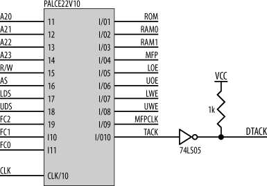
Address Decoder
Logic to perform address decoding and the generation of separate read and write strobes is implemented in a PAL. In each case, ![]() (Address Strobe) of the processor
(Address Strobe) of the processor

is used as an indication of a valid address present on the bus. The address-decode equations are as follows:
   ROM = /(/AS * /A23 * /A22)
   RAM0 = /(/AS * /A23 * A22 * /LDS)
   RAM1 = /(/AS * /A23 * A22 * /UDS)
   MFP = /(/AS * A23 * /A22)
With the exception of the MFP, which generates its own ![]() ,
, ![]() for all other devices is generated as part of the address decoding. Since
for all other devices is generated as part of the address decoding. Since ![]() from the PAL must be OR-tied with
from the PAL must be OR-tied with ![]() from the MFP, it must be driven from an open-collector gate. Therefore, we generate an active-high acknowledge (which we’ll designate TACK) from the PAL and invert this through a 74LS05 open-collector inverter.
from the MFP, it must be driven from an open-collector gate. Therefore, we generate an active-high acknowledge (which we’ll designate TACK) from the PAL and invert this through a 74LS05 open-collector inverter.
The PAL equation to generate TACK is simply:
TACK = (/AS * MFP)
Therefore, TACK is active (high) whenever the processor accesses its address space, so long as it is not accessing the MFP. If the address strobe is high, or if there is an access to the MFP, then TACK is low. The TACK output from the PAL is inverted through an open-collector 74LS05 and “OR-tied” (directly connected together) with ![]() from the MFP.
from the MFP. ![]() requires a pull-up 1 kΩ resistor, since this input must have a sharp rise time. A block diagram is shown in Figure 18-7.
requires a pull-up 1 kΩ resistor, since this input must have a sharp rise time. A block diagram is shown in Figure 18-7.
No provision for generating a ![]() is made because our simple address decoding allocates all of the address space. If we had any unused regions of the memory space, we would use our address decoder to generate a
is made because our simple address decoding allocates all of the address space. If we had any unused regions of the memory space, we would use our address decoder to generate a ![]() when accesses to the unused regions were made.
when accesses to the unused regions were made.

The PAL equations to generate separate read and write strobes for the memory chips are:
   UWE = /(/UDS * RW)
   LWE = /(/LDS * RW)
   UOE = /(/UDS * /RW)
   LOE = /(/LDS * /RW)
The connections for the PAL are shown in Figure 18-8. Additional addresses are brought into the PAL to allow for future changes to the memory map. The processor’s clock (CLK) is used by the PAL to generate the clock for the MFP (MFPCLK).
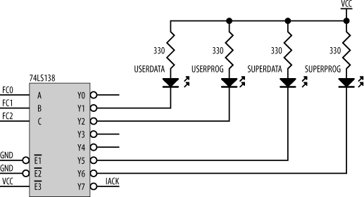
The function code outputs (FC0-FC2) can be decoded using a 74LS138 demultiplexer to drive three LEDs (Figure 18-9). These provide a visible indication of processor status. The function codes could also be used by the address decoder if you wanted to have separate user and supervisor address spaces. Many of the more sophisticated peripheral chips (such as the MFP) require the processor to acknowledge when they have generated an interrupt. The 74LS138 also uses the function codes to generate an interrupt acknowledge (IACK) for peripherals, since the function codes also indicate an IACK condition.
I/O
The MK68901 Multifunction Peripheral (MFP) provides a serial port, as well as basic parallel I/O functions, a 16-source interrupt controller, and four 8-bit timers. The MK68901 has an internal oscillator that drives the internal timers. A timer output (TD0) is fed back into the MFP as the clock for the serial interface. The internal oscillator must therefore run at a frequency appropriate for RS-232C. An external 3.6864 MHz crystal drives the oscillator. This input clock can be divided up by the MFP, providing the appropriate baud rates for the serial port. The serial lines from the MFP are converted to RS-232C voltage levels by a MAX3232 level shifter. A 9-pin, D-type connector provides access to the RS-232C signals. The parallel I/O lines and timer inputs and outputs are also made available through a 26-pin IDC connector.
The schematic for the MFP is shown in Figure 18-10.

Memory
The system is designed with 256K of EPROM and 512K of static RAM. The connections to the SRAM are shown in Figure 18-11. Note that since the data bus of a 68000 is 16 bits wide, two SRAMs are required. For 68000-based derivatives with 32-bit external data buses, four memory chips would be required in parallel. Note how half the data bus goes to one chip and the other half goes to the other chip.
Now, note the address lines going to the SRAMs. The lowest address bit from the processor is A1, and this is connected to the A0 inputs of the SRAMs, and so on. Since the processor accesses external memory in 16-bit words, A1 represents the least significant address bit. In other words, as you move from word to subsequent word in memory, it is A1 that increments. However, A0 is the least significant address bit of the SRAMs, but since the two SRAMs together form a 16-bit word of memory, the A0 of the SRAMs must connect to A1 of the processor. The other address bits follow on from that starting point.

Similarly, the connections for the ROMs are shown in Figure 18-12.
Wait States
Depending on the speed of your processor and the access times of your memory and peripheral chips, it may be necessary to introduce wait states into the 68000’s memory cycle. Wait-state generation follows basically the same principle for processors that support asynchronous memory cycles. The processor will have an input (sometimes more than one) that will cause it to delay the memory cycle, giving slower

devices time to respond. In the case of the 68000, that input is ![]() . To insert a wait state for a given device, we need to detect an access to that device and hold
. To insert a wait state for a given device, we need to detect an access to that device and hold ![]() inactive for the required additional clock cycles. In other words, we need to use the chip select for a given device to delay
inactive for the required additional clock cycles. In other words, we need to use the chip select for a given device to delay ![]() going low. The circuit to do this is simple and is best done inside a PAL or other programmable logic device. This facilitates changing the wait-state generator if faster parts are used in the design at a later stage. The wait-state generator consists of a series of D-type flip-flops[*] (Figure 18-13). Each flip-flop represents an additional clock cycle that the transfer acknowledge is delayed.
going low. The circuit to do this is simple and is best done inside a PAL or other programmable logic device. This facilitates changing the wait-state generator if faster parts are used in the design at a later stage. The wait-state generator consists of a series of D-type flip-flops[*] (Figure 18-13). Each flip-flop represents an additional clock cycle that the transfer acknowledge is delayed.
Between memory cycles, the address strobe, ![]() , goes high. It is first inverted and then connected to the active-low
, goes high. It is first inverted and then connected to the active-low ![]() input of each of the flip-flops. Thus, the output of each of the flip-flops is driven high between each memory cycle. This resets them from any previous cycle. The address decoder generates a chip select for the particular device, and this is connected to the D input of the first flip-flop. So, on each successive clock pulse, the
input of each of the flip-flops. Thus, the output of each of the flip-flops is driven high between each memory cycle. This resets them from any previous cycle. The address decoder generates a chip select for the particular device, and this is connected to the D input of the first flip-flop. So, on each successive clock pulse, the 0 provided by the chip select is clocked through from

one flip-flop to the next. After four clock pulses, the 0 has arrived at the Q output of the last flip-flop. The inverted output of this flip-flop, ![]() , becomes a
, becomes a 1. This is then output by the PAL to be inverted by the 74LS05 open-collector inverter to provide ![]() for the processor. For additional wait states, add more flip-flops. For several devices requiring different numbers of wait states, use their combined chip selects to feed the D input of the first flip-flop; then “tap” into the wait-state generator at different stages for the required delay. Each of these taps is gated with the respective chip select to enable/disable that output before they are all recombined to generate a unified acknowledge for the processor.
for the processor. For additional wait states, add more flip-flops. For several devices requiring different numbers of wait states, use their combined chip selects to feed the D input of the first flip-flop; then “tap” into the wait-state generator at different stages for the required delay. Each of these taps is gated with the respective chip select to enable/disable that output before they are all recombined to generate a unified acknowledge for the processor.
Most processors that support wait states now include inbuilt, software-configurable wait-state generators. This makes the task of designing the system logic much simpler.
In the next chapter, we’ll take a look at a different sort of embedded processor—one based on a Digital Signal Processing (DSP) architecture.