Chapter 17. MAXQ
We will find a way, or we will make one
—Hannibal, 218 B.C.
In this chapter, we’ll look at an innovative new processor architecture introduced to the world in 2004. Dallas Semiconductor, a subsidiary of Maxim (http://www.maxim-ic.com), developed the 16-bit MAXQ microcontrollers to target the low-cost, low-power embedded applications market. The architecture is aimed directly against Microchip’s PIC, Atmel’s AVR, Texas Instruments’ MSP430, and the 8051 architecture offered by many manufacturers (including Dallas Semiconductor itself). The MAXQ is an interesting contender for top RISC microcontroller. It’s fast, has a lot of functionality, and is very low-powered. At the time of writing, the User’s Guide for the MAXQ is 230 pages long. Obviously, this processor has a lot of features, too many to be thoroughly covered here. Therefore, I’m going to simply concentrate on the basic design for a MAXQ-based system. Let’s start by seeing what makes the MAXQ so different and so interesting.
Architectural Overview
The stated design goal for the MAXQ was to achieve a high performance-to-power ratio. In other words, the aim was to maximize the processor’s throughput of instructions while minimizing the current draw. Many RISC processors achieve single-cycle execution but do so through the use of an instruction pipeline. In a pipelined architecture, the execution unit is comprised of many stages. At any one time, several instructions will be in the process of being decoded and executed. Thus, with a pipeline, although a given instruction may take several cycles to execute, the processor is able to have an instruction terminate on each cycle (Figure 17-1).
Each cycle moves each instruction further along the pipeline, from fetch to termination (and result). The disadvantage of a pipeline is that a call or jump instruction means that all instructions following in the pipeline are not needed and the pipeline must be reloaded from a new location (where the jump/call was directed). So, while

pipelining can achieve single-cycle execution, it falls down in a big way unless the code is linear.
The MAXQ does not have an instruction pipeline, yet it still achieves single-cycle execution, with the exception of long jumps and calls and some extended register accesses. Now, you may say, “So what’s the difference?” since pipelined processors have problems with jumps and calls too. The difference is that a pipelined processor executing a jump means that not only is the jump not single-cycle, but it will cause a disruption to the pipeline affecting the following instructions. With the MAXQ, this is not the case. Only the jump or call is not single-cycle, and all subsequent instructions execute without incurring the delay of a pipeline reload.
The MAXQ achieves this by having instruction-decode and execution units that are much simpler than those found on many other processors. How simple? Well, the MAXQ has only one instruction (move), but that one instruction has multiple functions, depending on the source and destination operands. By having only one instruction, a classical decode unit is not required. (You already know what the instruction is going to be, so what’s there to decode about it?) Hence, the execution of instructions is reduced to determining source and destination, and whether additional hardware operations are triggered as part of the move. The source and destination bits of an instruction merely activate internal data paths, and this happens as the instruction is fetched.
The basic format for a MAXQ instruction is fdd dddd ssss ssss, where f is the format bit, d represents the destination-field bits, and s represents the source-field bits. When the format bit is a 1, the instruction moves data from one index module to another. When the format bit is a 0, an immediate 8-bit value is loaded into an index module (Table 17-1).
In the MAXQ architecture, the index modules are not necessarily specific registers, and herein lies the flexibility of the architecture. A given working accumulator may actually be represented by more than one index module. One index module will target the accumulator and perform an addition operation, while another index module will target the same accumulator yet perform a subtraction. In this way, two different operations are specified by two index modules, even though they both target the same register. Clever, isn’t it?
Tip
A few years ago, I designed an experimental zero-operand processor
(as a soft core) that also implemented single-cycle execution without pipelines. A zero-operand processor has its registers configured as a stack, and all instructions implicitly operate on the stack. An add instruction, for example, takes the top two stack entries (registers r0 and r1), adds them, and stores the result back to the top of the stack (r0). Since the source and destination are always known, operands can be pre-fed to the ALU, which computes all possible operations in parallel. An incoming instruction simply selects an appropriate ALU result or operation. In many ways, this conceptual simplicity is comparable to the MAXQ but is the other side of the same coin. The MAXQ uses one instruction with multiple index modules, whereas the zero-operand processor has many instructions but only one source/destination.
See Chapter 3 for more information about stack-based languages.
Like the PIC and AVR, the MAXQ is a Harvard-architecture processor, with separate code and data spaces. Overall, the MAXQ is a very nice processor, and one that I’m sure will gain market share as time passes.
With that in mind, let’s see how simple it is to design a MAXQ-based embedded computer. As you will see, although this is a powerful processor, when it comes to the “hard work” of design, there’s not much to it!
Schematics
A major problem common in utilizing a microcontroller in a mixed-signal environment (one that combines both digital and analog components) is the noise the digital subsystem introduces. Higher processor performance normally results in greater noise in the analog section, unless great pains are undertaken to minimize these effects. Thus, achieving high throughput is often contrary to the goal of keeping the analog circuits as noise-free as possible. The MAXQ implements intelligent clock management that reduces noise by enabling clocks only to those subsystems that require them, and only when they require them. In this way, the overall digital noise is reduced considerably. The MAXQ processor requires two crystals, a 16 MHz crystal (X1) for the main CPU clock and a 32.768 kHz watch crystal (X2) for the timers. Figure 17-2 shows the MAXQ2000F processor with its support components.
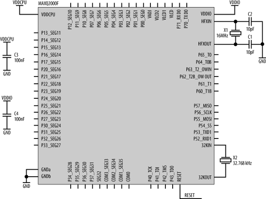
The MAXQ processor requires two power supplies, VDDCPU (2.5 V) and VDDIO (3.6 V), each decoupled to ground with 100 nF ceramic capacitors. The 2.5 V supply may be generated using a MAX1658 (Figure 17-3). This is a general-purpose regulator, the output of which is adjustable via bias resistors. These resistors, R1 and R2, set the output to +2.5 V. It is important that these resistors are precise, so choose resistors with 1% tolerance. The input and output of the regulator are each decoupled with 10 uF capacitors. The MAX1658 can operate on an input voltage (VIN) of between 2.7 V and 16.5 V, supplying up to 350 mA to the embedded computer system.
A similar circuit is used to generate the 3.6 V supply required by the MAXQ’s I/O subsystems (Figure 17-4). Note the different resistor values required to generate 3.6 V rather than 2.5 V.
The MAXQ has an internal power-on reset generator, kicking the processor to life at power-up. No external reset circuit is required. If a manual reset is required, a push- button switch may be used to pull the RESET line low. However, it is important to note that RESET is a bidirectional line. The MAXQ also uses this signal as an output to indicate that a reset condition (possibly generated internally) is being serviced.


This can be used by the system designer to reset external peripherals as well (if required).
The various ports, labeled Px, provide access to the MAXQ’s I/O. As well as providing digital I/O, they also serve dual purposes. Port 5 provides a SPI interface as well as a serial port. The SPI interface may be connected to any SPI-based peripheral. The serial port requires a level shifter such as a MAX3232, as shown in Figure 17-5. The transmitter (TXD1) and receiver (RXD1) of the MAXQ connect to the receiver and transmitter pins on the MAX3232.

Port 5 of the MAXQ provides access to JTAG signals for in-system programming and debugging. Figure 17-6 shows the pinout for a JTAG header. This is the same pinout used on the Maxim MAXQ development system, allowing you to use the same environment for your embedded computer.

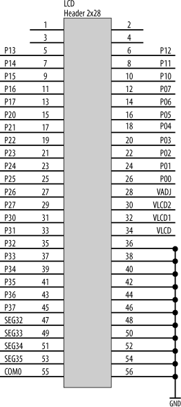
Ports 1, 2, and 3 double as an interface to a 36-segment (numerical) LCD. Figure 17-7 shows the connections to a header for the LCD ribbon cable.
The MAXQ is a versatile and fast 16-bit processor, and the family is due to be expanded by Maxim. If you’re looking for a low-powered, yet very capable processor for an embedded application, take a close look at the MAXQ. You’ll find it’s an impressive little processor.