Chapter 4. Electronics 101
...in reality, nothing but atoms and void
—Democritus
In writing this book, my hope is to bring to you an understanding of the design process involved in producing an embedded computer system. To this end, I have kept the electronics, the chips, and the systems I have used as simple as possible. I want you to understand the big picture without getting lost in detail. But, however simple I keep the computer designs, you won’t get very far without at least a very rudimentary understanding of electronics. So what I want to do in this chapter is give some basic background theory to guide you on your way. Electronics is a truly vast and complicated multidisciplinary field, and it is not possible to cover even a thousandth of it here. I won’t even attempt to. What I will do is give you an understanding of the basic principles necessary for embedded computer engineering in a simplified, and hopefully easy to understand, way. The rest of the vast mountain, I will leave unvisited. If you want to learn more, pick up a copy of Paul Horowitz and Winfield Hill’s The Art of Electronics (Cambridge University Press). It’s a great introductory text.
Voltage and Current
It’s all about electrons. It is from their very name that we derive the term electronics. Electrons are subatomic particles with a negative charge. They are bound to positively charged atomic nuclei through Coulombic attraction. The classical physics view was to think of electrons “orbiting” the nucleus, analogous to planets orbiting in a solar system. While not at all correct,[*] it makes it easier to visualize what goes on. The strength by which electrons are bound to the nucleus varies from atomic element to atomic element, and from molecule to molecule. Substances are either conductors , insulators , or semiconductors . In a conductor, such as a metal, the energy required to shift an electron from one nucleus to another is negligible, and the electrons may easily exchange with nearby atomic nuclei. In effect, the metal is a collection of nuclei surround by a “sea” of semi-free electrons. In an insulator, the opposite is true. The energy required to shift an electron from a nucleus is excessive, and so electrons tend to stay put. In a semiconductor, the substance may act either as a conductor or as an insulator, depending on external influences. By controlling the external influences, you change the conductivity of the substance and therefore change the way electrons move within that substance. In effect, a semiconductor is a switch that may be controlled by other semiconductors. It is this basic principle that is the basis of all modern electronics. It is the cornerstone upon which everything digital is founded.
The flow of electrons through a conductor or a semiconductor is known as current . Current is measured in Amperes, more commonly called just plain Amps (with the unit symbol “A,” equation symbol “I”). For an electron to move through a conductor,[*] there must be a “vacancy” at the next nucleus into which it can shift. (If the next nucleus has a full complement of electrons, the Coulombic repulsion of those electrons will prevent any others from slotting in.) Semiconductor physicists term these vacancies holes . An electron shifting into a neighboring hole leaves a new hole behind it. This new hole is then filled by another electron further down the line, which, in turn, creates another new hole. So current flow is, in effect, a movement of electrons in one direction and a “movement of holes” in another. The electrons are negatively charged, and the holes may be thought of as positive charges. (A missing electron at a nucleus means that the positive charge of the nucleus isn’t fully canceled, and so a net positive charge exists at that location.) So while electrons move from negative to positive, the holes move from positive to negative, and it is the movement of holes (rather than electrons) that we refer to when we talk about current. Current flow, which we work with in electronics, is deemed to be from positive to negative. For continued current flow, there must be a continuous circular flow of electrons in one direction and holes in the other direction. It is from this circular flow that we derive the term circuit .
For current flow to occur between two points, there must exist an imbalance between electrons at one end and holes at the other. The size of this imbalance is known as the potential difference , or voltage difference , between two points. (It is also sometimes termed “the voltage drop across an electronic component.”) The unit of voltage difference is the Volt (unit symbol “V”). The greater the voltage difference, the greater the opportunity for current flow. It is very important to note that voltage refers to the difference between two points. A voltage cannot exist in isolation. Although you will sometimes see a statement like “the voltage at this point is...,” it is taken as given that it is relative to some common reference point, usually ground (the zero-volt reference point).
Analog Signals
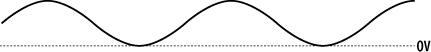
An analog signal can have an amplitude of any voltage within a range, unlike a digital signal, which can be in one of two defined voltage states (either high or low). Figure 4-1 shows a typical analog signal (in this case, a sine wave).
The voltage of a signal may vary over time, or it may be constant. If the voltage varies, it may repeat at regular intervals, in which case the signal is said to be periodic. The period is the interval of time it takes the signal pattern to repeat (for example, from one wave crest to another). The frequency of the signal is the number of times per second that the pattern repeats.
Frequency is measured in Hertz (Hz) and relates to the period in the following way:
Frequency = 1 / Period
Thus, a signal with a period of 1 ms has a frequency of 1 kHz.
A unipolar signal (Figure 4-2) has component voltages that are either all positive or all negative. A bipolar signal (Figure 4-3) has both positive and negative voltages.
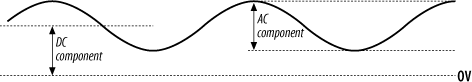
A typical analog signal will have both an AC component and a DC component (Figure 4-4). The DC component is the fixed voltage of the signal. The AC component is a varying voltage imposed on the DC component. The AC component is sometimes referred to as the peak-to-peak amplitude of a signal and is denoted with the suffix “pp.” For example, an AC component of 5 V would be written as 5 Vpp.
Power
A voltage difference is generated by a difference in potential energy between two points. Therefore, to generate a voltage, you use a device that can create such an energy difference. Such devices may be mechanical (generators), converting motion into a potential difference by electromagnetics; photovoltaic (solar cells); or chemical (batteries). Conversely, a voltage difference (and therefore current flow) can be used to produce mechanical movement (motors), light emission (light bulbs, LEDs), and heat (toasters, Pentium 4 processors).
Power is the amount of work per time (Joules per second) and is measured in Watts (unit symbol “W”). The equation for calculating power is simply:
P = V * I
No electronic device is 100% efficient (far from it!), and so it will consume power as it performs its task. The power consumed by a device may be calculated using the above equation, from the voltage difference across the device and the current flowing through the device. A typical embedded computer may consume a few hundred mW (milliWatts) of power, but it can vary quite considerably. A large and powerful embedded machine may use several tens (or even hundreds) of Watts, while a tiny embedded controller may use just microWatts.
Reading Schematics
You won’t get very far in electronics unless you know how to draw and read schematics. They crop up everywhere, and understanding them is a must. The schematics are like an architect’s blueprint. They show what components will be used in a circuit and how they are connected together. The schematics may also include other information such as construction directives. A schematic may have a list of revisions indicating what changes have been made to the original design. These are commonly called Engineering Change Orders (ECOs). As a design grows and changes over time, it’s a good idea to keep track of what changes were made and, more importantly, why they were made. Just as commenting source code is important, so is keeping track of the ECOs.
You will come across two types of schematics. There are the schematics you see in datasheets, books (like this one), and other technical documents. These schematics will just show the circuit (or partial circuit) and maybe a note or two, and that’s all. The other sort of schematic is the actual drawing(s) used to generate a Printed Circuit Board (PCB). These schematics represent a full system design and will often have a title block located in the lower right of the sheet, indicating what the sheet represents, who drew it, and when. Figure 4-5 shows a sample title block.

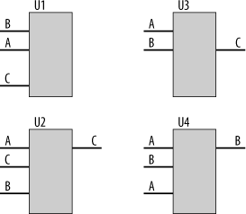
Essentially, there are two types of objects on a schematic: component symbols and nets . Nets are the wires that show what is connected to what, and component symbols represent physical devices. A component symbol will have a component name and a component type. For example, a memory chip may have the name U3 and have a component type AT45DB161. The component name is simply a reference label, much like a variable name in source code. It’s important to keep component labels unique. Having two devices labeled U3 on a schematic may cause a great deal of confusion for the design automation software. The component type is the actual part number used by the component manufacturer.
It is common practice with component names to use common prefixes for components of the same type. For example, resistors have the prefix R. You will see resistors on a schematic labeled R1, R2, R3, etc. Similarly, capacitors carry the prefix C, inductors L, diodes D, transistors Q, crystals X, and connectors and jumpers J. Semiconductors often carry the prefix U, but not always. Logic gates and other small, nondescript semiconductors may have the prefix U, but larger semiconductors may have a more informative name. For example, a processor may be labeled PROC, while four memory chips may carry the names RAM0, RAM1, RAM2, and RAM3. Giving larger devices more meaningful names often makes schematics easier to understand. However, that being said, a lot of people still give every semiconductor the U prefix.
Figure 4-6 shows an example component with a net.
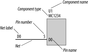
As well as the name and part number, the component will also have an array of pins. The pins may have a number, a name, or both. The number indicates the physical pin on the chip to which the schematic pin is referring, and the name gives an indication of its function. Some components, such as resistors, do not have pin names or numbers shown.
Component pins may have names and symbols that indicate their characteristics. Figure 4-7 shows an example component with a variety of pin types.

Pin 1 is a generic pin. Pin 2 has a bar over the pin name that indicates that it is active low
. This means that a logic 0 on this pin will activate its function, while a logic 1 will deactivate it. Pin 2’s name is ![]() , which typically means chip select
. In other words, this pin is used to activate the chip. Most peripherals and memory chips have a chip-select input. Chip selects are important since there are many memory and peripheral chips within a computer system. It is through the chip select that the processor will enable the chip so that it can write data to it or read data from it. Some devices have an input called
, which typically means chip select
. In other words, this pin is used to activate the chip. Most peripherals and memory chips have a chip-select input. Chip selects are important since there are many memory and peripheral chips within a computer system. It is through the chip select that the processor will enable the chip so that it can write data to it or read data from it. Some devices have an input called ![]() , which means chip enable
. It’s exactly the same as a chip select. They are just two different names for the same function.
, which means chip enable
. It’s exactly the same as a chip select. They are just two different names for the same function.
The little triangle on pin 3 indicates that it is an edge-triggered input. This simply means that the input responds to a change in signal.
Pins 4 and 8 are ground (GND) and power (VCC), respectively. “VCC” and “VDD” are used to label voltage sources for powering the circuits. The terminology originates from transistors and solid-state electronics, where “collectors” (VCC) and “drains” (VDD) are common parlance. You don’t need to worry about what the names mean, just know that when you see “VCC” or “VDD,” we’re talking about supply voltages.
Pin 7 is an output that is active high, and pin 6 is an output that is active low. Note the circle on pin 6. This indicates that it is an inverted output. The fact that it has the same name as pin 7 indicates that pin 6 is the inversion of the output of pin 7. Finally, pin 5 is labeled “NC.” This is commonly used to represent “No Connect,” which means that this pin has no function. No net should be connected to it. (Very rarely, you’ll also see a pin name “Do Not Wire.” It means the same thing.) However, just because you see a pin name “NC” doesn’t mean that you should assume that it is a no-connect. It may just be that the chip manufacturer labeled the pin NC for some other reason. As always, check the datasheet carefully for each device.
A net may be drawn between two components or may simply have a net label giving the net a name and indicating that it is connected to every other net with the same name. With complicated schematics, it may not be practical to show every wire that must be connected. There would simply be wires going everywhere, and the resulting schematic would be impossible to understand. Therefore, it is common practice to simply use the net labels to locally name a net, and this alone is enough to indicate what is connected to what (Figure 4-8).
Signals that are functionally related, such as buses, are drawn using a bus net (Figure 4-9).
It is common practice to use more than one schematic sheet for a design. Just as a program is broken up into functions, with commonly used code placed in libraries, designs are also broken into functional units, allowing subsystem reuse in multiple designs. For example, the same power-supply circuit may be used in several different embedded computer designs. By placing the power-supply circuit on its own sheet,
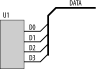
that same subsystem design may be reused in many designs. Ports are used to indicate when a schematic’s nets are connected to another schematic sheet. Figure 4-10 shows a component with connections to off-sheet objects. In this case, the “D0:D3” port is a bidirectional bus, the “A0:A3” port is an output bus from this sheet (and therefore an input to another sheet), and the “MODE” port is an input net to this sheet.

Figure 4-11 shows nets crossing each other. The vertical net on the left is not connected to the horizontal net. It simply crosses over on its way to another part of the circuit. The vertical net on the right is connected to the horizontal net, and this is indicated by a junction dot.

In some hobbyist electronics magazines and old textbooks, you’ll sometimes see nets with “little bridges” as they cross other nets (Figure 4-12). This is definitely not the way to draw it—very unprofessional, very uncool.
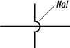
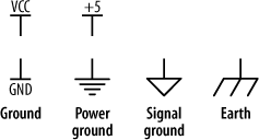
Figure 4-13 shows common power ports . These indicate connections to voltage sources (power supplies) and grounds. The ground symbols all mean a potential of zero volts. The different symbols are used to differentiate between different ground networks. In microprocessor schematics, you’ll commonly see the two leftmost ground symbols (usually only one or the other) and rarely see the other two.
Tip
By the way, always place your power ports vertically, never horizontally. Horizontal power ports are like source code that isn’t indented-- frowned upon as the work of the Unenlightened. Also, voltage ports (like VCC) should point up, while ground ports should point down. A ground port should never be pointing skyward, nor should a voltage port be pointing down. For a professional engineer, they’re a vexation to the spirit.
Resistors
Even a conductor (such as a metal wire) is not 100% efficient at conducting current flow. As current flows through the wire, energy will be lost as heat (and sometimes light). For very small currents, this energy loss is negligible, but for large currents, the loss can cause the conductor to become quite hot (an effect utilized in toasters) or glow brightly (light bulbs). This loss of energy results in a voltage difference across the wire (or component). The component is said to resist the current flow. This resistance (also known as impedance , although impedance is somewhat more complex than simple resistance) is measured in Ohms (unit symbol “Ω,” equation symbol “R”). In schematics, it is common to leave off the Ω symbol, so 100 kΩ is usually written as just 100 k.
Tip
On a schematic, a 4.7 kΩ value is often not written as 4.7 k, but rather as 4k7. The reason is that it is too easy for a decimal point to be missed, or lost when the document is photocopied. The solution is to place the multiplier (“k”) in the position of the decimal point. Resistors such as 24.9 Ω are written as 24R9.
This convention is used by design engineers in most of the world. However, in North America it is only sometimes followed.
The relationship between voltage, current, and resistance is known as Ohm’s Law , and is given by:
V = I * R
For a fixed resistance, a varying voltage will produce a varying current, while a constant voltage will produce a constant current. Hence, a varying voltage source is known as an Alternating Current source (or AC), while a constant voltage source is known as a Direct Current source (DC). An AC voltage is normally specified as VAC, while a DC voltage is either VDC or more often just V.
Tip
The stuff that comes out of your wall socket is AC, and is nominally 110-120 VAC (at 60 Hz) if you live in North America; 100 VAC if you’re in Japan (50 Hz in the eastern half [Tokyo] and 60 Hz in the western half [Osaka, Kyoto, and Nagoya]); and 220-240 VAC (at 50 Hz) if you’re in Australia, New Zealand, the UK, or Europe. All digital electronics, and that includes computers, use DC internally and operate at typical voltages of either 5 V or 3.3 V. (Some digital electronics will operate at voltages as low as 1.8 V or lower.) The power supply of the computer (or TV or stereo or...) converts the high-voltage AC supply into the lower DC required by the electronics. The AC adaptor or plug pack (charger) for your cell phone is also an example of a power supply.
For a given voltage difference, the smaller the resistance, the larger the current flow. Conversely, the bigger the resistance, the smaller the current flow. In this way, resistance can be used to limit the current flow through a particular part of a circuit. Special components, known as resistors, are produced for precisely this purpose. Resistors are part of a family of devices known as passive components .
Figure 4-14 shows “through-hole” resistors. From top to bottom, they are 0.5 W, 0.25 W, and 0.125 W, respectively.
Figure 4-15 shows surface-mount resistors. Surface-mount technology is now far more common than the older “through-hole” style of component. The components shown in Figure 4-15 are a “1206” footprint (left) and a “0603” footprint (right).

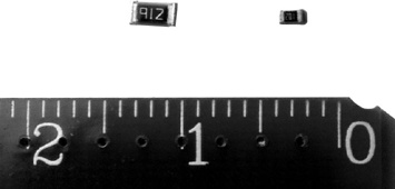
There are smaller footprints than these available, but if you’re hand-soldering, you are more likely to suffer a nervous breakdown before you successfully solder the component to the circuit board!
The schematic component symbols for a resistor are shown in Figure 4-16. Both symbols mean the same thing. The more commonly seen symbol is on the left.
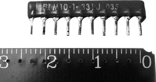
A resistor may be used to pull up (or pull down) a signal line to a given voltage level. If you have many pull-up resistors in your circuit, all of the same value, it may be convenient to use a resistor network, or “resnet,” shown in Figure 4-17. Resnets combine several resistors (typically eight, but available in other sizes as well) in a single package. All the resistors are tied to one pin, which is connected to the power supply such that all resistors act as pull-ups.
Figure 4-18 shows a pull-up resistor and a push button. When the button is open (not pressed), there is no current flow through the resistor, and, therefore, the voltage at VOUT is (in this case) +5 V. (Since there is no current flow through the resistor, there is no voltage drop across it.) When the button is pushed, VOUT is connected to ground, and, consequently, current will flow through the resistor. This simple circuit can be used to switch an input between two logic level thresholds.

Resistors may be daisy-chained together to increase resistance. This is known as a series connection (Figure 4-19).
The combined total resistance is given by the relation:
RTOTAL = R1 + R2
The current flow through any of the components in series connection will be the same for each component. In other words, the current flowing through the first resistor will be the same as that flowing through the second resistor. This derives from Kirchhoff’s Current Law .
Tip
The current flowing through a given circuit point is equal to the sum of the currents flowing into that circuit point, and is also equal to the sum of currents flowing out of that circuit point.
In other words, what flows in must flow out.
Series resistors may be used to create a voltage divider (Figure 4-20) to provide an intermediate voltage.
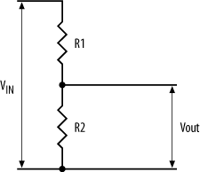
The output voltage is given by:
VOUT = VIN * R2 / (R1 + R2)
For example, if the input voltage is 5 V, and the two resistors are both 1 kΩ, then the output voltage is:
   VOUT    = 5V * 1k / (1k + 1k)
      = 5V * 1k / 2k
      = 5V * 0.5
      = 2.5V
As you would expect, a voltage divider using equal resistors halves the input voltage.
Resistors combined in parallel (Figure 4-21) will decrease the total resistance.

The combined total resistance is given by the relation:
RTOTAL = 1 / (1/R1 + 1/R2)
The voltage drop across R1 must be the same as the voltage drop across R2. However, unless R1 is equal to R2 (and there is no requirement for them to be so), the current flow through each will be different. This is derived from Kirchhoff’s Voltage Law .
A potentiometer (also known simply as a “pot,” “trimmer,” or “trim pot”) is just a variable resistor. The schematic symbol for a pot is shown in Figure 4-22. Pots are normally mechanical components and are manually adjusted. Your stereo probably uses pots for its volume, bass, and treble controls. The brightness and contrast knobs for monitors and LCDs are also potentiometers.
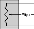
A standard potentiometer consists of two terminals (the upper and lower pins in the diagram) that connect to either end of a resistor. A third terminal, known as the wiper , moves up or down the resistor, effectively tapping into the voltage present at a given point. Move the wiper one way, and the amount of resistance the wiper sees is increased. Move it the other way, and the resistance decreases.
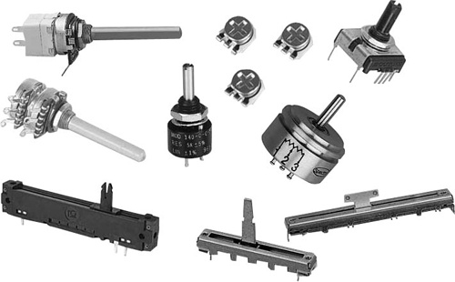
There are many different types of pots available. Figure 4-23 shows several pots, including a slider pot and two types of rotary pot. Usually, the pot is fitted inside the equipment casing with the wiper shaft poking through an appropriate hole or slot. A knob is then screwed to the shaft.
Mechanical pots come in a variety of resistance ranges, and their accuracy is not particularly good. They may be used to provide an adjustable voltage output (Figure 4-24) or simply to vary the resistance used in an analog circuit.
As a simple example, you could use a pot to vary the intensity of a LED by varying the current flow through it. A circuit to do this is shown in Figure 4-25. Here, the fixed resistance between the LED’s anode and the pot’s wiper is 330Ω. By adjusting the wiper, we add to this resistance, thus decreasing the current flow through the LED and reducing its brightness.


Note how one terminal of the pot is unconnected. This is fine, since in this case we are not using the pot to provide an intermediate voltage between two values. Rather, we are simply using the pot as a variable resistor, increasing the impedance between the wiper and VDD.
Capacitors
While a resistor is a component that resists the flow of charge through it, a capacitor stores charge. Capacitance is measured in Farads (or more formally, “Faradays”) with an equation symbol “C” and a unit symbol “F.” Typical capacitors you will use range in value from uF (micro-Farads) down to pF (pico-Farads).
The relationship between current, capacitance, and voltage is given by:
I = C * dV/dt
where dV/dt is the rate of voltage change over time.
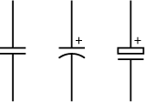
The schematic symbols for capacitors are shown in Figure 4-26. The component on the far left is bipolar, while the other two are unipolar. A unipolar capacitor has a positive lead and a negative lead, and it must be inserted into a circuit with the correct orientation. Failing to do so will cause it to explode. (Unipolar capacitors have markings to indicate their orientation.) A bipolar capacitor has no polarity.
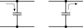
Applying a voltage across a capacitor causes the capacitor to become charged. If the voltage source is removed, and a path for current flow exists elsewhere in the circuit, the capacitor will discharge and thereby provide a (temporary) voltage and current source (Figure 4-27).
This is an extremely useful characteristic. A given voltage source may have a DC component (a fixed voltage) and an AC component (a ripple voltage superimposed). (Here, “component” does not mean a physical device, but rather a fractional part of a voltage.) The capacitor becomes charged by the DC component of the voltage source to a given level and is then alternately charged and discharged with the AC component. In effect, the capacitor averages out the peaks and troughs of the AC component and, as a result, removes the AC ripple from the voltage source. This is known as the capacitor decoupling the AC and DC components of the voltage source. This is a common technique used to remove electrical noise from power supplies, for example.
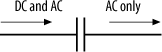
The flip side of this is that a capacitor can also be used to block the DC component of a voltage, allowing only the AC component to pass through (Figure 4-28).
Capacitors may also be used in series or parallel (Figure 4-29).

The relationship is the opposite of what it is for resistors. In the series case, the total capacitance is calculated by:
CTOTAL = C1 * C2 / (C1 + C2)
In the parallel case, the total capacitance is given by:
CTOTAL = C1 + C2
Types of Capacitors
There are over a dozen different types of capacitor, each based on a different technology. The ones you are most likely to come across are ceramic , electrolytic, and tantalum.
Ceramic capacitors are small in size and small in value. They range from a few picofarads (pF) up to around 1 uF. They are commonly used as decoupling capacitors for power-supply pins of integrated circuits and as bypass capacitors in crystal circuits (among other uses).
Electrolytics look like small cylinders and are used primarily for decoupling power supplies. They range in value from 100 nF to several F (and we’re talking big capacitors here). Their accuracy is terrible. Their actual value can vary quite a bit from what it is supposed to be. Therefore, they are not used where critical tolerances are required. Use them only where “ballpark” values are sufficient.
The other problem with electrolytics is that they age, and the older they get, the worse they become. Expect a circuit using electrolytics to eventually fail. Having said that, most consumer electronics still use them heavily, and for one reason—they are very cheap. By the time they’ve failed, the product will be well out of the warranty period. However, electrolytics will outlast the useful lifetime of your average computer product. You’ll have upgraded your PC to a newer model long before its electrolytics have passed on.
Tip
The most common cause of failure in old radios and hi-fi gear is that the electrolytics have failed. You can often pick up a very cheap bargain at a garage sale. Ten minutes with the soldering iron and you’ve replaced the electrolytics, and what “doesn’t work anymore” suddenly comes back to life as good as new. Well, most of the time anyway.
Tantalum capacitors are somewhat larger than ceramics but not as physically large as electrolytics. In through-hole devices, they have the appearance of small, shiny plastic bulbs. Surface-mount tantalums look much like all other surface-mount capacitors: small ubiquitous rectangles. They range in value from around 100 nF up to several hundred uF. They are commonly used to decouple power supplies. They are more accurate than electrolytics, meaning their actual value is closer to their stated value. I always use tantalums in preference to electrolytics in my designs where possible. I like my machines to last.
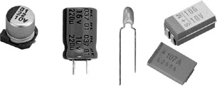
Some common capacitors are shown in Figure 4-30.
RC Circuits
Combining resistors and capacitors can yield some interesting and useful effects. A resistor-capacitor combination is known as an RC circuit, and it can take one of three forms. The first form is where the resistor and capacitor are in parallel (Figure 4-31).
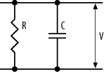
Now, what does this do? A voltage (V) applied across the pair will charge the capacitor (as well as some current flowing down through the resistor). When the applied voltage is removed, the capacitor will discharge through the resistor. The resistor will limit the rate of discharge, since it limits current flow. From Ohm’s Law, we have:
I = - V / R
(The negative voltage is because we’re discharging the capacitor.) Now, the current flow out of a capacitor is given by:
I = C * dV/dt
So, we have:
dV/dt = - V / RC
Integrating this with respect to time, with zero initial conditions, gives us:
V = e-t/RC
This gives us the discharge waveform shown in Figure 4-32, which represents the voltage across the capacitor.
A parallel RC circuit will provide an exponential decay in the output voltage. The value for t when the output voltage is at 37% of the maximum is known as the time constant for the circuit and is simply the product of R and C:
t = R * C
For example, a parallel RC circuit where the resistor is 100 kΩ and the capacitor is 10 uF gives a time constant of 1 second.
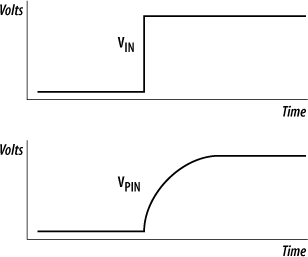
The second form of RC circuit is the series RC circuit, shown in Figure 4-33.
When a voltage is applied at the input to the RC circuit (on the left), current will flow through the resistor and the capacitor will begin to charge. However, the resistor limits current flow and therefore will limit the rate at which the capacitor charges.


Now, the current flowing into the capacitor is again given by the relation:
I = C * dV/dt
This current is the same as that which is flowing through the resistor, and by Ohm’s Law, we have that this current is given by:
I = (VIN - VOUT) / R
where VIN - VOUT is the voltage drop across the resistor. Combining these two equations gives us the differential equation:
dV / dt = (VIN - VOUT) / RC
Integrating this gives us the voltage at the capacitor as:
VOUT = VIN (1 - e-t/RC)
Again, this is an exponential equation; however, this time it represents an exponential charging of the capacitor. The waveform for the voltage at the capacitor is shown in Figure 4-34.
In this case, the time constant is the time for the voltage at the capacitor to reach 63% (total - 37%) of the input voltage. As before, this time constant is simply the product of R and C.

This form of RC circuit is a simple type of low-pass filter . This is a circuit that provides a path to ground for high-frequency components of a signal, thereby attenuating them from the main signal, while the low-frequency components suffer far less attenuation. This type of circuit is very useful for removing high-frequency noise that may be superimposed on a signal.
A given processor or peripheral chip will have a small amount of input capacitance on each input pin. This, combined with the small inherent impedance of a circuit connection and the input impedance of the pin, means that an applied digital voltage to the pin will actually appear as an exponential rise, rather than as a sharp (digital) edge (Figure 4-35). These effects are minimal but can be significant in high-speed circuits or where several devices are connected to the same signal line and the overall input capacitance is not insignificant.
The effect of lead inductance can contribute second-order characteristics, such as those shown in Figure 4-36. These inductive effects create “ringing” when a sudden voltage change is applied. Inductors will be discussed shortly.

The third form of an RC circuit is shown in Figure 4-37.

This type of circuit is a simple form of a high-pass filter , since it passes only the high frequencies through to the output. The capacitor in such a circuit is known as a blocking capacitor.
Inductors
Inductors are passive components that are essentially coils of conductive wire. The schematic symbol for an inductor is shown in Figure 4-38. Inductance is measured in Henries, with an equation symbol “L” and a unit symbol “H.”
The voltage across an inductor changes the current flow through it, measured with the following relation:
V = L * dI / dt
Whereas applying a current to a capacitor caused the voltage to build across it, the opposite is true for an inductor. Applying a voltage across it builds current flow through it, and the resulting energy is stored in the inductor as a magnetic field. When the applied voltage is removed, the field collapses and returns the stored energy as a voltage spike.
Figure 4-39 shows a series R-L circuit.

The voltage across the resistor (VR) and the voltage across the inductor (VL) are shown in Figure 4-40. When a voltage is applied at VIN, the voltage across the resistor is initially small, whereas the voltage across the inductor is large. As the current flow through the inductor builds, the voltage across the resistor increases, while the voltage across the inductor diminishes accordingly.
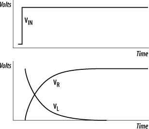
Figure 4-41 shows a series R-L-C circuit.
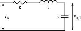
The response (VOUT versus time) of an R-L-C circuit to a step input is shown in Figure 4-42.

Figure 4-43 shows an R-L-C circuit where all the components are in parallel.

The step response of this circuit is shown in Figure 4-44.
Inductors are commonly used in switching voltage regulators (Chapter 5) and are also employed (in combination with a resistor and capacitor) as filters to remove unwanted frequency components from a signal. Inductive effects exist in many components, and inductive voltage spikes are the bane of the embedded-system designer.

Transformers
Transformers are related to inductors. A transformer consists of two coils of wire, known as the primary and the secondary, that are closely coupled magnetically. The schematic symbol for a transformer is shown in Figure 4-45.

An AC current flowing through the primary will generate an associated electro-magnetic field. The strength of the field is proportional to the number of turns in the coil of the primary. Because the secondary is within this field, the field will generate a current flow through (and therefore a voltage difference across) the secondary. Since the secondary has a different number of windings in the coil than the primary, the field generated by the primary will create a different voltage and current in the secondary (provided, of course, that the secondary is part of a circuit so that current can flow). Therefore, a transformer can be thought of as a voltage multiplier (or divider). The ratio of the number of turns in the primary and secondary will determine the voltage multiplication.
Since transformers are usually exceptionally efficient, most of the power in the primary is transferred across to the secondary. If the secondary increases the voltage of the primary, then the secondary’s current will correspondingly be smaller than in the primary. Conversely, if the voltage across the secondary is less than the primary, the current through the secondary will therefore be larger than in the primary.
Transformers are commonly used inside power supplies to convert the high line voltage (110 VAC or 240 VAC, depending on where you live) to a much lower voltage for use by electronic systems and other appliances. They also provide isolation between the powered system, and the high-voltage supply.
A transformer with a ratio of n turns has an increase in impedance of n 2. Therefore, another use of transformers is to provide a way of changing the impedance of a transmission line. For example, an Ethernet port will have a transformer between the interface chip and the cable.
Diodes
Diodes are semiconductor devices that are extremely useful. They have the interesting characteristic that they will pass a current in one direction but block it from the other. They can be used to allow currents to flow from one part of a circuit to another but prevent other currents from “backwashing” where you don’t want them.
The schematic symbol for a diode is shown in Figure 4-46. The arrow indicates the direction of conduction. The arrow represents the anode , or positive side, of the diode, while the bar represents the cathode , or negative side, of the diode. A higher voltage on the left of the component will allow current to be passed through to the right. However, a higher voltage on the right will be prevented from causing current flow to the left.
Diodes have a forward voltage drop when conducting. This means there will be a voltage difference between the anode and the cathode. For example, a diode may have a forward voltage drop of 0.7 V. If this diode is part of a larger circuit and the voltage at the anode is 5 V, then the voltage at the cathode will be 4.3 V.
Diodes come in a variety of shapes and sizes. Figure 4-47 shows a small power diode. The white stripe indicates the cathode (negative) end of the diode.
Diodes are useful for removing negative voltages from a signal, a process known as rectification . Four diodes may be combined to form a bridge rectifier, as shown in Figure 4-48. The bridge “flips” the negative components of the wave, so that only a positive voltage is present at the output. A capacitor on the output can be used to smooth the rectified wave.
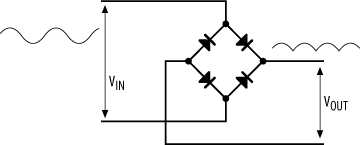
Such configurations are commonly used on the power inputs of embedded computers and other digital systems. A voltage can be applied across the inputs on the left, with no regard as to which should be positive or negative. The bridge rectifier ensures that a positive voltage will always be conducted to the upper right, and at the same time current flow is returned from the lower right through the bridge rectifier to whichever lefthand connection is negative.
If you’ll forgive the pun, the most commonly seen diode is the LED (Light Emitting Diode). The schematic symbol is shown in Figure 4-49, and a through-hole LED is shown in Figure 4-50. All diodes produce a small amount of light as a consequence of their operation (although you don’t normally see it because of the diode casing); it’s just that LEDs are especially good at it.


There is a limit to the amount of current that can pass through a LED. Exceeding this current will potentially damage or destroy the LED. For this reason, LEDs are used in conjunction with a current-limiting resistor. Figure 4-51 shows such a circuit. Some LEDs will incorporate a current-limiting resistor internally. However, most do not, so it is important to check the manufacturer’s datasheet. Generally, you’ll need to include the resistor, and calculating the required value (R) is easy.
Let’s say that the LED has a forward voltage drop of 1.6 V and a current limit of 36 mA. We need to select a resistor that will limit the current flowing through the LED

to this value. In our circuit, the LED and resistor are in series, and the total voltage across them is 5 V. So, if the LED has a voltage drop of 1.6 V, then we can easily calculate the voltage drop across the resistor:
   VR = 5 - 1.6
        = 3.4 V
So, if the voltage drop across the resistor is 3.4 V, and we need to limit the current to 36 mA, then using Ohm’s Law we can calculate a value for R:
   R = V / I
     = 3.4 / 0.036
     = 94.44 Ω
A 100 Ω resistor will therefore do fine and will result in a brightly glowing LED. If you want lower-intensity light, you just need to limit the current further, and you would therefore use a larger resistor. Note that since 36 mA is the maximum current the LED can handle, we will always need a resistor that keeps the current flow below this. Therefore, we always opt for a larger R.
The power that the resistor must dissipate is given by the relation:
   P = V * I
     = 3.4 * 0.036
     = 0.1224 W
Resistors are available with different power-dissipation ratings. It is important to choose a resistor with the correct rating. In this instance, we would use a 0.125 W resistor.
The ubiquitous power-on LED you see in your home appliances works in this exact same way. This simple LED circuit (or variations of it) drives the LEDs on your PC’s front panel, on your VCR and DVD player, your cell phone, and a host of other appliances. Many traffic lights and railroad signals are replacing conventional bulbs with arrays of LEDs, as the LEDs last longer and produce more light (per area).
LEDs are available in red, green, yellow, blue, and white. The last two colors are very hard to produce and therefore relatively expensive.
There are two more types of diodes about which it is useful to know: Zener diodes and Schottky diodes (Figure 4-52).
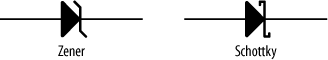
Zener diodes exhibit a characteristic known as dynamic resistance , or small-signal resistance . The voltage drop across a Zener diode will not change as the current through it changes. In effect, it acts as a variable resistor whose resistance is current-dependent. Zener diodes are commonly used to provide a reference voltage (Figure 4-53).
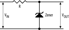
From Ohm’s Law, we have:
(VIN - VOUT) = I * R
Now, if VIN changes, it logically follows that the current will also change. So we can modify our equation thus:
(VIN -
The Zener acts as a source of dynamic resistance, which we’ll designate Rd. Now what we have is effectively a voltage divider. So, our equation for VOUT is:
Schottky diodes are also known as hot-carrier diodes and behave like conventional diodes, save for a very small forward voltage drop. They are commonly used in power-supply circuits and signal rectification for this reason.
Crystals
Finally in our component tour, we come to crystals . Just as their name suggests, they are small blocks of quartz (silicon dioxide). Quartz crystal is a type of material known as a piezo-electric. This is a substance that generates a voltage when it is stressed (compressed, stretched, twisted). This effect is utilized in microphones. The sound vibrates the piezo-electric material, and it produces a small AC voltage that is directly proportional to the original sound that created it. This voltage is then amplified for broadcast, recording, or processing.
The opposite effect is also true for piezo-electric materials. Apply a voltage and the piezo-electric material will contort or vibrate. Some speakers use piezo-electric materials to produce sound. (However, most use other techniques, such as electro-magnetics.) Most loud buzzers are based on piezo-electrics.
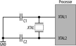
Now, the neat thing about quartz is that for a block of a given size, it will vibrate at a given (and fixed) frequency. As such, it can be used as an oscillator to generate a sine wave, which in turn can be used to generate timing signals for microprocessors and other digital circuits. Just about every computer system will have a crystal (or two) somewhere on its circuit board, generating the timing that ultimately drives the whole machine. That crystal is simply a small block of quartz, plated at either end with wires attached and encased in a metal can.
The schematic symbol for a crystal is shown in Figure 4-54, and a real crystal is shown in Figure 4-55.

Crystals require a drive circuit to make them go. These tend to be a bit temperamental and don’t always oscillate at the frequency you expect, due to a range of effects that are hard to track down. Fortunately, there are two easy ways around this problem. The first is that most processors (and other chips requiring timing) have internal oscillator circuits. All you need to do is add the external crystal (and maybe a capacitor or two), and it will work beautifully. For those chips that don’t make life quite so easy, you can get complete oscillator modules, which include the crystal and drive circuit. All you need to do is give them power and ground, and they too will work beautifully.
Clocks and Oscillators
All microprocessors (and quite a few other digital devices too) require a clock. A clock is an output from an oscillator that runs the processor and all system events related to the clock. (And just in case you’re wondering, this “clock” has nothing to do with the time of day. Think of it as a stream of digital pulses.) The clock frequency is normally expressed in kiloHertz (kHz), MegaHertz (MHz, 1,000 kHz), or GigaHertz (GHz, 1,000 MHz). The clock frequency of a processor is also known as its clock speed . (Note the capital “H” in Hz. It is never “hz,” always “Hz.”)
A given processor will have a maximum and a minimum clock frequency. This specifies the range in which the oscillator driving the processor can operate. A processor with a minimum clock speed of zero is said to have static operation , or DC operation . This means that the processor can have its clock stopped and still be able to resume operation at a later time with no ill effect. If the minimum operating frequency of a processor is specified to be greater than zero, then that processor is said to have dynamic operation . If the oscillator frequency falls below the minimum of a dynamic processor, then that processor may suffer corruption of its registers.
The clock speed of a processor relates to how quickly a processor can execute software. A processor running at a faster clock speed will execute software faster than a processor of the same type running at a slower clock speed. But clock speed is not the whole story in terms of processor speed. One processor architecture may take 32 clock cycles to execute an instruction, whereas another processor may complete one instruction every clock cycle. So, even though these two processors are running at the same clock speed, the latter will be significantly faster than the former.
There are several ways of generating a clock. Which is appropriate depends largely on the processor you are using. Some processors expect a digital (square-wave) clock input. For a processor running at common frequencies, and this includes most processors, the best choice is to use a device called an oscillator module (Figure 4-56). These four-pin components provide a square-wave clock output at a given frequency, requiring only power and ground connections. These simplify the system design, as they are “plug and go” devices.
Many processors (including all the microcontrollers I can think of) contain oscillator circuitry and generally require only the addition of an external crystal and bypass capacitors (Figure 4-57). The capacitors remove higher-order harmonics from the oscillation.
Power versus speed
Often it is necessary to design a system with minimal power consumption. This may be done to reduce the heat produced by a system or to make the system portable.

The more current that devices within a system use, the hotter they become. Too much heat will cause them to stop working. While it is possible to provide cooling subsystems and temperature monitors, the better approach is simply to reduce the power consumption and therefore the heat. When a system is powered by batteries, the lower its current draw, the longer the batteries will last. For these reasons, low-powered design is advantageous.
Most of the current usage of a digital system occurs during transitions of state—in other words, during the clock edges. The more frequent the clock edges, the more the average current usage goes up. Therefore, the faster a processor runs, the more power it consumes. Conversely, the lower the processor’s operating voltage, the less its power consumption is. Many embedded processors are available in lower-voltage versions. Power consumption can also vary between architectures. An ARM processor running at the same clock speed and operating voltage as a Pentium will have considerably less power consumption. It is for this reason that ARMs are common in PDA devices.
Using chips with static operation allows the clock of the system to be slowed (or stopped), and since power consumption relates directly to speed, this can reduce the overall power usage of the machine. The clock may be slowed in several ways. First, the clock can be kept permanently slow. For an application that does not require a lot of computing power (a traffic-light controller, for example), a processor clock of 32 kHz (rather than, say, 20 MHz) may be used.
Alternatively, in systems that occasionally require heavy computation, the system clock may be slowed only when the processor is idle. Many laptop computers use this technique to reduce their power consumption. The processor runs at full speed when in use. If the system sits idle for 30 seconds, the clock is slowed down into the kHz range. If the system remains idle for several minutes, the clock is slowed down into the Hz range. Since the user is not actively working with the machine (that’s why it is idle), the user doesn’t notice any difference. The moment the processor is required to perform a task (such as when a key is pressed), the clock is switched back to full speed and normal operation is resumed.
Tip
Palm computers use this technique very effectively. The machines are event-driven, meaning they do something when the user taps the screen, or when an I/O device requires servicing. Therefore, in between events, the processor slows down considerably. When an event occurs, the system switches back to full speed, processes the event, and then returns to idle mode. The processor spends far more time in idle mode than in operating mode, and, therefore, the battery use is minimal. It is by using this technique that Palms get such long operating life from their batteries. It is also why you never see (or shouldn’t see) computationally intensive applications on Palm computers. The batteries would be flat in no time.
Some computer systems may even halt the clock completely until the processor is required, at which point an external device reactivates the system clock.
Many processors have SLEEP and HALT modes, reducing the processor’s power consumption. Some processors extend this to SLEEP, NAP, DOZE, SNOOZE, etc., each with a different level of power usage and each requiring a different period of time for the processor to “awaken.” (The deeper the sleep, the longer it takes for the processor to resume operation.)
This concludes the discussion of electronic components. One major type of component that I haven’t covered is transistors. They have been left out simply because they are not commonly seen in embedded systems, and a proper coverage of transistors would occupy a large volume in its own right. If you are interested in learning about transistors, there are plenty of excellent books available. Just visit your local technical bookstore or cruise the Internet.
Digital Signals
Being an electronic circuit, the operation of a computer is about voltages and current flow. Understanding the basic principles of voltages and current flow within the computer is mandatory if you’re going to produce a working system. Common operating voltages inside a computer are normally either 5 V or 3.3 V. For some low-power or exceptionally fast computers, voltages may be as small as 1.8 V or lower.
An output pin of a digital device can be in one of three states. It can be high (logic 1), low (logic 0), or tristate (high-impedance, also known as floating). A logic high is defined as the output voltage at the pin being higher than a given threshold. When a device’s pin is outputting a high, it is said to be sourcing current to that connection. Similarly, a logic low is where the output voltage is below a given threshold, and the device’s pin is said to be sinking current. Typically, components can sink more current than they can source.
A tristate pin is outputting neither a high nor a low. Instead, it becomes high-impedance (high-resistance) such that current flow in or out of the pin is negligible. It is, in effect, invisible to other components to which it is connected. For example, within a computer system there may be several memory devices connected to the data bus. When a particular device is being read, its data outputs will be either high or low (corresponding to the bit pattern being read back). All other memory devices in the system, because they are not being accessed, will have tristate data buses. They take no part in the read transaction between the processor and the accessed memory device.
The threshold for logic high and the threshold for logic low can vary from device type to device type. For an input device to recognize a given signal as high or low, the output device must provide that signal within the appropriate limits. The thresholds can vary but are always consistent across devices of the same logic families. Back in the good old days, there were a limited number of logic families, and each device within a family conformed to the thresholds of that family. Life, and designing digital systems, was easier. Now, with the quest for ever lower-powered devices and the desire for devices to be as versatile as possible, the thresholds for logic high and logic low are considerably diverse. So the input low threshold for a given chip may not match the output low threshold for the chip to which it is to be connected. Therefore, it is vitally important to check the datasheets of all the components you are using and ensure they will work together.
When a device outputs a logic high, and its output voltage is greater than the high threshold for the input device, current will flow from the output pin to the input pin. The output device is sourcing current, while the input device is sinking current.
Conversely, for certain types of digital logic, when a device outputs a logic low, and its output voltage is lower than the low threshold of the input device, current will flow from the input pin to the output pin, even though the output device is the one controlling the voltage. The output device is sinking current, while the input device is sourcing current (Figure 4-58).

The magnitude of the current flow is important. A given device will have limitations on how much current it can sink or source. Exceeding this current limit can permanently damage an integrated circuit. It is therefore important to calculate the current flows within your system and ensure that all the requirements are met.
Electrical Characteristics
Pick up any chip datasheet and you will find three sections, labeled Absolute Maximum Ratings, DC Electrical Characteristics, and AC Electrical Characteristics. These are vitally important, but often poorly understood. So let’s see what it all means, and how you work with that information to produce a reliable and effective embedded system. Let’s look at the Absolute Maximum Ratings first.
Absolute Maximum Ratings
The very first thing you’ll see in the electrical characteristics section is something labeled Absolute Maximum Ratings . A chip will be designed to operate under certain nominal conditions, and exceeding those conditions during normal operation is not advised. But what happens if you do go beyond those parameters? At just what point will you really kill the chip? The Absolute Maximum Ratings tell you just that. They show you how far you can stress the chip, and (sometimes) for how long, before the device will fail.
An example of the Absolute Maximum Ratings for a chip, in this case a Dallas Semiconductor DS87C550 microcontroller, is shown in Table 4-1.
|
Parameter |
Rating |
|
Voltage on any pin relative to ground |
-0.3 V to (VCC + 0.5V) |
|
Voltage on VCC relative to ground |
-0.3 V to 6.0 V |
|
Operating temperature |
-40°C to +85°C |
|
Storage temperature |
-55°C to +125°C |
|
Soldering temperature |
160°C for 10 seconds |
So what does it all mean? Let’s work through it. The first row of the table refers to the voltage range any pin of this microcontroller can tolerate. Normally, the voltage applied to a pin (be it signal or power) will range from zero volts (ground) to VCC (in the case of the DS87C550, this is +5 V). The Absolute Maximum Ratings tell us that if a pin falls to below -0.3 V (in other words, pretty much any negative voltage), the chip may be damaged. Similarly, if a pin has an applied voltage greater than VCC + 0.5 V, then it will also be damaged. Now, a lot of people would interpret VCC + 0.5 V to be +5.5 V since the nominal VCC is +5 V. This is not necessarily the case. VCC + 0.5 V means 0.5 V above the actual VCC that you’re using to power the chip, not the nominal value of +5 V. If you’re running a DS87C550 from a supply of +4.5 V (perfectly valid), then the absolute maximum rating for an input is not +5.5 V but +5 V. The design engineer (that’s you) must ensure that no device connected to this microcontroller will exceed those parameters.
Tip
Note that not all chips have an Absolute Maximum Rating for input voltage as tight as the DS87C550. I can think of one memory chip that operates from a +2.7 V supply voltage but can tolerate signals as high a +6 V on its inputs. As always, it’s vitally important to check the datasheet for each device you are using to see what is and what is not possible.
Let’s look at an example where we have two embedded systems, each using an identical 87C550 microcontroller, cooperating as part of a larger system. In the first embedded system, designed by Company A, the 87C550 is powered from a +4.5 V supply. In the second embedded system, produced by Company B, the 87C550 is running on a +5.5 V supply. Both of these supply voltages are valid, and perfectly allowable within the specifications of these chips. Now, an output high from the second embedded system may be (and probably will be) +5.5 V. (The datasheet only gives a minimum value for an output high of +2.4 V, meaning that in reality, a high could be anywhere in the range +2.4 V to VCC.) An input high to the first embedded system’s microcontroller cannot exceed VCC + 0.5 V:
   Max input = VCC + 0.5V
          = 4.5V + 0.5V
          = 5V
So, an output high from the second embedded system could very well exceed the maximum input rating of the first, even though they are based on identical chips. This illustrates the importance of checking everything carefully and thinking about what is going on within the system. An engineer assuming that both systems will work together since they use the same microcontroller would be wrong and would very likely kill the first system.
The second row of the table tells us the maximum power supply the chip can tolerate. In the case of this processor, although its nominal operating voltage is +5 V (listed elsewhere in the datasheet), it can actually run off a supply as high as +6 V. However, exceeding +6 V on the power pins will probably damage the chip. Similarly, applying a negative voltage to a power pin will also damage the chip.
The operating temperature (row three in our table) specifies the temperature range at which this chip will operate reliably. If it is colder than -40°C, then the chip may physically fail, or the software it is executing may crash. Similarly, if the microcontroller is run in an environment where the temperature exceeds +85°C, then the chip will also fail. Now, the operating temperature is different from the storage temperature (row four of the table). The device can be stored reliably at any temperature between -55°C and +125°C without stressing the chip and potentially causing it to fail.
Tip
In some datasheets, you’ll see operating temperature listed as junction temperature, referring to the temperature within the semiconductor. It effectively means the same thing.
The final entry in the table indicates the maximum soldering temperature that the chip can tolerate. In this case, it can withstand +160°C for 10 seconds. Now, 160 degrees is not that hot as far as soldering irons go. In truth, the chip can probably tolerate much higher temperatures than this, but only for significantly shorter periods of time. So, if I was to solder this chip using a standard iron, the final row of the table tells me that I need to be quick when soldering each pin, and that I should let the device cool down between soldering each pin. Holding a hot iron against each pin for several seconds will build up temperature within the chip and will turn a complicated, functioning integrated circuit into a mere ornament in the middle of the circuit board.
DC Characteristics
The DC characteristics specify the voltages and currents pertaining to the chip during normal operations. In datasheets, you’ll often see the DC characteristics (and sometimes the Absolute Maximum Ratings) referred to as commercial grade, industrial grade, or military grade. These indicate the robustness of a particular part and its ability to withstand harsh environments. A military-grade part will be able to withstand higher temperatures, have better noise immunity, and have a longer operating life. In some cases, the military-grade part will have radiation hardness, meaning that it can survive and continue to operate after exposure to radiation. The downside is that a military-grade part will be more expensive, sometimes harder to get, and may not operate at as high a speed as its commercial-grade cousin. Now, you may think that unless you’re designing military hardware, you’ll have no need of military-grade parts. However, if you’re designing equipment that will be used in space, at high altitude, or in the Arctic or Antarctic, where temperature variations are extreme and radiation levels can be high, military grade may be the better choice.
The DC characteristics data is presented in a table format. An example, showing some typical entries (for an imaginary chip), is given in Table 4-2. Now, I say “typical” in the loosest sense of the word. For each chip manufacturer, there is a different way of presenting the data. But you’ll work it out, as it’s not that hard once you know what to look for.
|
Parameter |
Symbol |
Min |
Typ |
Max |
Unit |
|
Supply voltage[a] |
VDD |
3 |
- |
5.5 |
V |
|
Input-low voltage |
VIL |
VSS |
- |
0.15VDD |
V |
|
Input-high voltage |
VIH |
0.25VDD |
- |
VDD |
V |
|
Output-low voltage[b] |
VOL |
- |
- |
0.6 |
V |
|
Output-high voltage[b] |
VOH |
VDD - 0.7 |
- |
- |
V |
|
Supply current[c] |
IDD |
- |
0.8 |
1.4 |
mA |
|
Sleep current[d] |
Isleep |
- |
10 |
25 |
nA |
|
Input capacitance |
|
|
|
TBD |
pF |
[a] Referenced to VSS [b] 3 ≤ VDD ≤ 5.5 V [c] Oscillator = 4 MHz [d] Oscillator = 32 MHz | |||||
The supply voltage tells us the operating voltage needed to supply the chip. The symbol is simply a label, used in other parts of the datasheet to refer to this parameter. In this case, the supply voltage is a minimum (Min) of 3 V and a maximum (Max) of 5.5 V. This means that we can run this chip using a supply voltage anywhere within this range. The typical (Typ) column is left blank, indicating that there is no preferred supply voltage within this range. Sometimes you’ll see a chip with a minimum supply voltage of 4.5 V, a maximum of 5.5 V, and a typical supply voltage of 5 V. What this tells us is that this part requires a 5 V supply (indicated by the Typ value) but can tolerate a range of 0.5 V on either side of this. Some manufacturers will use nominal (Nom) in place of typical. It means the same thing. The footnote (a) pertaining to this entry indicates that the supply voltage is referenced to VSS. This may seem like an obvious thing, but it is important. VSS is typically ground (zero volts), but it need not be. In exceptional circumstances, the design may require that VSS be some voltage other than ground. Hence the footnote says that the supply voltage must be 3 V to 5.5 V above VSS. So, if VSS were 2 V, for example, our supply voltage would be 5 V to 7.5 V. (Remember that it is the voltage difference that is important.)
The next two rows show us what voltage levels are required on an input pin to register as a low (0) or a high (1). Note that these are not absolute values, but are referenced to VSS and VDD.
The output low voltage is given as a maximum of 0.6 V, with no minimum or typical values. This means that when this chip is outputting a low, it will be no greater than 0.6 V. Although no minimum is given, it can be assumed that the minimum is VSS. The chip would not output a low below this value. The footnote for this parameter and the next parameter indicates that the values given are for when the chip is operating from a supply voltage of between 3 V and 5.5 V. Such a range is typically written as “3 V ≤ VDD ≤ 5.5 V.” This just means that VDD lies between 3 V and 5.5 V.
The supply current has a typical value and a maximum value. For some manufacturers, the typical value is what you’ll see in reality. For other manufacturers, the typical value could best be described as “wishful thinking.” The real value is often closer to the maximum than the typical. The note tells us that the supply current given is for when the chip is running at 4 MHz. Since the current used by a device varies with speed, this parameter is only of limited use. Some manufacturers will give you an equation or a graph that allows you to determine supply current for any oscillator speed.
The sleep current shows how much juice this chip will draw when it is in “sleep” or “power down” mode. As you would expect, it is much less than the “awake” supply current given in the row above. But, look at the footnotes. The sleep current is given for an oscillator speed of 32 kHz, while the supply current is for an oscillator speed of 4 MHz. Some manufacturers do this deliberately to make their devices look better than they are, as this can mask the true nature of the part. (Remember that current drops with clock speed anyway.) This makes it hard to determine what the real current draw of the device will be in your application. Sure, the sleep current may be 10nA at 32 kHz, but it might be 0.5 mA at 4 MHz. Another trick manufacturers use is to provide a value for the supply current to the core (the CPU) but disregard the current used by all the onboard peripherals. It may look good on paper, but the reality could be quite different. The only way to be really sure is to build the thing into a system and measure it.
The final parameter in our example is input capacitance . Every input pin has a small capacitance, and this combines with the small inherent resistance of the signal traces (circuit board tracks) to act as an RC circuit. Earlier in this chapter, we saw how an input pulse into an RC circuit results in a rising voltage at the output. This means that although an input may quickly change from a low to a high, the input capacitance of the pin will provide a slight delay before the chip “sees” this change in input. You need to take this into account in your design, especially with respect to rapidly changing signals.
Now, in this particular example, the input capacitance is specified as “TBD.” This is the bane of the system designer. “TBD” means “To Be Determined.” In other words, this parameter wasn’t known at the time the datasheet was written. TBD can pop up in all sorts of places in datasheets and can be a real problem if you’re trying to design a machine. I remember one datasheet for a processor many years ago where every parameter, from supply voltage and current to voltage levels and timing, was listed as TBD!
Finally, be aware that technical data in some (not all) datasheets is theoretical only. In other words, the design engineers for the chip or part calculated what the values should be using their supercomputer (or abacus or Tarot cards). Other manufacturers actually go to great pains to measure their technical parameters, and even provide you with detailed explanations of the test conditions. They take a very thorough approach, and you can use their parts in confidence. Maxim and Texas Instruments are examples of two such companies, although there are many more.
AC Characteristics and Timing
A timing diagram is a representation of the input and output signals of a device and how they relate to each other. In essence, it indicates when a signal needs to be asserted and when you can expect a response from the device. For two devices to interact, the timing of signals between the two must be compatible, or you must provide additional circuitry to make them compatible.
Timing diagrams scare and confuse many people and are often ignored completely. Ignoring device timing is a sure way of guaranteeing that your system will not work! However, they are not that hard to understand and use. If you want to design and build reliable systems, remember that timing is everything!
Digital signals may be in one of three states: high, low, or high-impedance (tristate). On timing diagrams for digital devices, these states are represented as shown in Figure 4-59.

Transitions from one state to another are shown in Figure 4-60.

The last waveform (High-High/Low) indicates that a signal is high and, at a given point in time, may either remain high or change to low. Similarly, a signal line that is tristate may go low, high, or either high or low depending on the state of the system. An example of this is a data line, which will be tristate until an information transfer begins. At this point in time, it will either go high (data = 1) or low (data = 0), as shown in Figure 4-61.
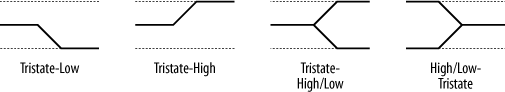
The waveforms in Figure 4-62 indicate a change from tristate to high/low and back again. These symbols indicate that the change may happen anywhere within a given range of time, but will have happened by a given point in time.

The waveform in Figure 4-63 indicates that a signal may/will change at a given point in time. The signal may have been high and will either remain high or go low. Alternatively, the signal may have been low and will either remain low or go high.
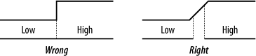
The impression given in many texts on digital circuits is that a change in signal state is instantaneous. This is not so. A transition is never instant; it can be several nanoseconds in duration, and there is considerable variation between different devices (Figure 4-64). The datasheet for each component will detail the transition times for that particular device.
Datasheets from component manufacturers specify timing information for devices. A sample timing diagram for an imaginary chip is shown in Figure 4-65.

The diagram shows the relationship between input signals to the device (such as ![]() ) and outputs from the device (such as Data). The numbers in the diagram are references to timing information within tables. They do not represent timing directly. Table 4-3 shows how a datasheet might list the timing parameters.
) and outputs from the device (such as Data). The numbers in the diagram are references to timing information within tables. They do not represent timing directly. Table 4-3 shows how a datasheet might list the timing parameters.
|
Ref |
Description |
Min |
Max |
Units |
|
1 |
CS Hold Time |
60 |
|
ns |
|
2 |
CS to Data Valid |
|
30 |
ns |
|
3 |
Data Hold Time |
5 |
10 |
ns |
Timing reference “1” (the first row of Table 4-3) shows how long ![]() must be held low. In this instance, it is a minimum of 60 ns. This means that the device won’t guarantee that
must be held low. In this instance, it is a minimum of 60 ns. This means that the device won’t guarantee that ![]() will be recognized unless it is held low for more than this time. There is no maximum specified. This means that it doesn’t matter if
will be recognized unless it is held low for more than this time. There is no maximum specified. This means that it doesn’t matter if ![]() is held low for longer than 60 ns. The only requirement is that it is low for a minimum of 60 ns.
is held low for longer than 60 ns. The only requirement is that it is low for a minimum of 60 ns.
Timing reference “2” shows how long it takes the device to respond to ![]() going low. From when
going low. From when ![]() goes low until this device starts outputting data is a maximum of 30 ns. What this means is that 30 ns after
goes low until this device starts outputting data is a maximum of 30 ns. What this means is that 30 ns after ![]() goes low, the device will be driving valid data onto the data bus. It may start driving data earlier than 30 ns. The only guarantee is that it will take no longer than 30 ns for this device to respond.
goes low, the device will be driving valid data onto the data bus. It may start driving data earlier than 30 ns. The only guarantee is that it will take no longer than 30 ns for this device to respond.
Timing reference “3” specifies when the device will stop driving data once ![]() has been negated. This reference has a minimum of 5 ns and a maximum of 10 ns. This means that data will be held valid for at least 5 ns, but no more than 10 ns, after
has been negated. This reference has a minimum of 5 ns and a maximum of 10 ns. This means that data will be held valid for at least 5 ns, but no more than 10 ns, after ![]() negates.
negates.
Some manufacturers use numbers to reference timing; others may use a label (Figure 4-66).

Some manufacturers will specify timing from when a signal becomes valid until it is no longer valid. Others specify timing from the middle of a transition to the middle of the next transition (Figure 4-67).

Logic Gates
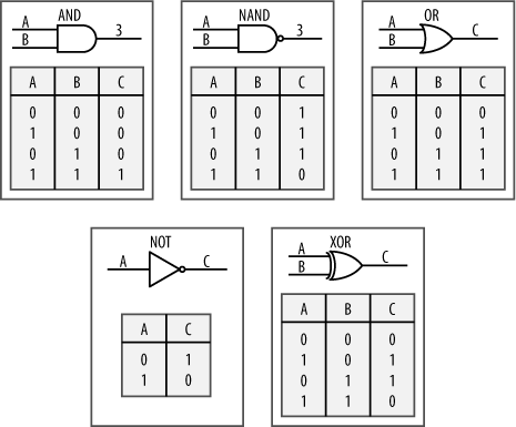
In days of old, computers (and other digital electronics) were built using discrete logic gates . Nowadays, these are somewhat rare, with programmable logic being the preferred option. However, it is not unusual to still see the odd logic gate in a schematic. For your reference, Figure 4-68 shows the most common gates and their truth tables. In each case, A and B are inputs, and C is the output.
The Importance of Reading the Datasheet
Before starting any design, you need to work out the basic requirements for your system (what it will do, how much it will cost) and select the major components you will need (such as a processor, I/O, and memory). Before you do anything else, obtain the datasheets for these components and read them from beginning to end. These can typically be found on manufacturers’ web sites. (Every chip used in this book was specifically chosen because it had full technical data available online.) Just go to the manufacturer’s web site and download the relevant documentation.
Once you’ve read the data thoroughly and feel you understand it, go back and reread it to pick up all the things you missed on the first pass. It’s much better to discover something critical that you’ve missed before you design and build a computer, rather than after.
Always make sure you have the latest datasheets and errata (datasheet bug lists) before you begin a design. Using a datasheet that is even a little bit old is not a good idea. It is not unusual for the electrical and technical specifications to change from time to time, so it’s critical that you use the latest (and most accurate) data.
It is very important that you understand how the devices work. When you are debugging your system, you have to know what to look for to know whether different parts of your computer are functioning. Don’t assume anything about the functionality of the devices. Read and check everything carefully, including voltage levels, basic timing, and anything else that may be relevant to the system.
Tip
If possible, a very useful thing to include in your design is a serial interface, even if you don’t need a serial port for the final application. A serial port is extremely useful for printing out diagnostic and status information from the system, and can be an indispensable diagnostic tool (for both hardware and software). The other mandatory debugging tool is the status LED. A flashing LED can tell you volumes about a machine being tested if the LED is used intelligently by the software and programmer. The more status LEDs you have, the better life will be!
Well, that completes the quick tour of this most very basic introduction to electronics. If you’re curious to know more, please seek out some more in-depth books on the topic. It really is a fascinating and complex field, worthy of fuller coverage than I am able to give here. Now that we’ve covered the basics of what the electrons are up to, in the next chapter we’ll look at providing power for your embedded system.
[*] The truth, as always, is far stranger. The quantum view is both beautiful and bizarre. For a simple and elegant introduction, read Richard Feynman’s brilliant QED (Quantum Electro Dynamics) (Princeton University Press).
[*] I’m treating a conducting semiconductor as though it were an ordinary conductor.