
Chapter 15. The AVR Microcontrollers
A really useful engine...
—W.V. Awdry
In this chapter, we’ll look at the Atmel AVR processor. Like the PIC, this processor family is a range of completely self-contained computers on chips. They are ideally suited to any sort of small control or monitoring application. They include a range of inbuilt peripherals and also have the capability of being expanded off-chip for additional functionality.
Like the PIC, the AVR is a RISC processor. Of the two architectures, the AVR is the faster in operation and arguably the easier for which to write code, in my personal experience. The PIC and AVR both approach single-cycle instruction execution. However, I find that the AVR has a more versatile internal architecture, and therefore you actually get more throughput with the AVR.
In this chapter, we’ll look at the basics of creating computer hardware by designing a small computer based on the AVR ATtiny15. We’ll also see how you can download code into an AVR-based computer and how it can be reprogrammed in-circuit. From there, we’ll go on to look at some larger AVR processors, with a range of capabilities.
Later in the chapter, we’re going to look at interfacing memory (and peripherals) to a processor using its address, data, and control buses. For most processors, this is the primary method of interfacing, and, therefore, the range of memory devices and peripherals available is enormous. You name it, it’s available with a bus interface. So, knowing how to interface bus-based devices opens up a vast range of possibilities for your embedded computer. You can add RAM, ROM (or flash), serial controllers, parallel ports, disk controllers, audio chips, network interfaces, and a host of other devices.
Most small microcontrollers are completely self-contained and do not “bring out” the bus to the external world. In this chapter, we’ll take a look at the Atmel AT90S8515 processor. It is the only processor of the AVR family that allows you access to the CPU’s buses. But first, let’s take a look at the AVR architecture in general.
The AVR Architecture
The AVR was developed in Norway and is produced by the Atmel Corporation. It is a Harvard-architecture RISC processor designed for fast execution and low-power consumption. It has 32 general-purpose 8-bit registers (r0 to r31), 6 of which can also act as 3 16-bit index registers (X, Y, and Z) (Figure 15-1). With 118 instructions, it has a versatile programming environment.

In most AVRs, the stack exists in the general memory space. It may therefore be manipulated by instructions and is not limited in size, as is the PIC’s stack.
The AVR has separate program and data spaces and supports an address space of up to 8M. As an example, the memory map for an AT90S8515 AVR processor is shown in Figure 15-2.

Atmel provides the following sample C code, which it compiled and ran on several different processors:
int max(int *array)
{
  char a;
  int maximum = -32768;

  for (a = 0; a < 16; a++)
    if (array[a] > maximum)
      maximum = array[a];
  return (maximum);
}
The results are interesting (Table 15-1).
This indicates that, when running at the same clock speed, an AVR is 7 times faster than a PIC16, 15 times faster than a 68HC11, and a whopping 28 times faster than an 8051. Alternatively, you’d have to have an 8051 running at 224 MHz to match the speed of an 8 MHz AVR. Now, Atmel doesn’t give specifics of which compiler(s) it used for the tests, and it is certainly possible to tweak results one way or the other with appropriately chosen source code. However, my personal experience is that with the AVR, you certainly do get significantly denser code and much faster execution.
There are three basic families within the AVR architecture. The original family is the AT90xxxx. For complex applications, there is the ATmega family, and for small-scale use, there’s the ATtiny family. Atmel also produces large FPGAs (Field-programmable Gate Arrays), which incorporate an AVR core along with many tens of thousands of gates of programmable logic.
For software development, a port of gcc is available for the AVR, and Atmel provides an assembler, simulator, and software to download programs into the processors. The Atmel software is freely available on its web site. The low-cost Atmel development system is a good way of getting started with the AVR. It provides you with the software and tools you need to begin AVR development.
The AVR processors at which we’ll be looking are the small ATtiny15, the AT90S8535/AT90S4434, and the AT90S8515.
The ATtiny15 Processor
For many simple digital applications, a small microprocessor is a better choice than discrete logic, because it is able to execute software. It is therefore able to perform certain tasks with much less hardware complexity. You’ll see just how easy it is to produce a small, embedded computer for integration into a larger system using an Atmel ATtiny15 AVR processor. This processor has 512 words of flash for program storage and no RAM! (Think of that the next time you have to install some 100 MB application on your desktop computer!) This tiny processor, unlike its bigger AVR siblings, relies solely on its 32 registers for working variable storage.
Since there is no RAM in which to allocate stack space, the ATtiny15 instead uses a dedicated hardware stack that is a mere three entries deep, and this is shared by subroutine calls and interrupts. (That fourth nested function call is a killer!) The program counter is 9 bits wide (addressing 512 words of program space), and therefore the stack is also 9 bits wide. Also, unlike the bigger AVRs, only two of the registers (R30 and R31) may be coupled as a 16-bit index register (called “Z”).
The processor also has 64 bytes of EEPROM (for holding system parameters), up to five general-purpose I/O pins, eight internal and external interrupt sources, two 8-bit timer/counters, a four-channel 10-bit analog-to-digital converter, an analog comparator, and the ability to be reprogrammed in-circuit. It comes in a tiny 8-pin package, out of which you can get up to 8 MIPS performance. We’re not going to worry about most of its features for the time being. That will all be covered in later chapters when we take a look at the I/O features of some larger AVRs. Instead, we’re just going to concentrate on how you use one for simple digital control.
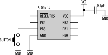
Using a small microcontroller such as the ATtiny15 is very easy. The basic processor needs very little external support for its own operation. Figure 15-3 shows just how simple it is.

Let’s take a quick run-through of the design (what there is of it). VCC is the power supply. It can be as low as 2.7 V or as high as 5.5 V. VCC is decoupled to ground using a 0.1 uF capacitor. The five pins, PB0 through PB4, can act as digital inputs or outputs. They can be used to read the state of switches, turn external devices on or off, generate waveforms to control small motors, or even synthesize an interface to simple peripheral chips. The digital I/O lines, PB0 through PB4, get connected to whatever you’re using the processor to monitor or control. We’ll look at some examples of that later in the chapter.
Finally, one input, ![]() , is left unconnected. On just about any other processor, this would be fatal. Many processors require an external power-on reset (POR) circuit to bring them to a known state and to commence the execution of software. Some processors have an internal power-on reset circuit and require no external support. Such processors still have a reset input, allowing them to be manually reset by a user or external system. Normally, the reset input still requires a pull-up resistor to hold it inactive. But the ATtiny15 processor doesn’t require this. It has an internal power-on reset and an internal pull-up resistor. So, unlike most (all) other processors,
, is left unconnected. On just about any other processor, this would be fatal. Many processors require an external power-on reset (POR) circuit to bring them to a known state and to commence the execution of software. Some processors have an internal power-on reset circuit and require no external support. Such processors still have a reset input, allowing them to be manually reset by a user or external system. Normally, the reset input still requires a pull-up resistor to hold it inactive. But the ATtiny15 processor doesn’t require this. It has an internal power-on reset and an internal pull-up resistor. So, unlike most (all) other processors, ![]() on the ATtiny15 may be left unconnected. In fact, on this particular processor, the
on the ATtiny15 may be left unconnected. In fact, on this particular processor, the ![]() pin may be utilized as a general-purpose input (PB5) when an external reset circuit is not required. One important point: the normal input protection against higher-than-normal voltage inputs is not present on
pin may be utilized as a general-purpose input (PB5) when an external reset circuit is not required. One important point: the normal input protection against higher-than-normal voltage inputs is not present on ![]() /PB5, since it may be raised to +12 V during software download by the program burner. Therefore, if you are using PB5, you must take great care to ensure that the input never exceeds VCC by more than 1 V. Failing to do so may place the processor into software-download mode and thereby effectively crash your embedded computer.
/PB5, since it may be raised to +12 V during software download by the program burner. Therefore, if you are using PB5, you must take great care to ensure that the input never exceeds VCC by more than 1 V. Failing to do so may place the processor into software-download mode and thereby effectively crash your embedded computer.
The AVR processors (and PICs too) include an internal circuit known as a brownout detector (BOD). This detects minor fluctuations on the processor’s power supply that may corrupt its operation, and if such a fluctuation is detected, it generates a reset and restarts the processor. There is also an additional reset generator, known as a watchdog, used to restart the computer in case of a software crash. It is a small timer whose purpose is to automatically reset the processor once it times out. Under normal operation, the software regularly restarts the watchdog. It’s a case of “I’ll reset you before you reset me.” If the software crashes, the watchdog isn’t cleared and thus times out, resetting the computer. Processors that incorporate watchdogs normally give software the ability to distinguish between a power-on reset and a watchdog reset. With a watchdog reset, it may be possible to recover the system’s state from memory and resume operation without complete re-initialization.
Now the other curious aspect of the above design is that there is no clock circuit. The ATtiny15 can have an external crystal circuit. (On the ATtiny15, PB3 and PB4 function as the crystal inputs, XTAL1 and XTAL2). But our design doesn’t have a crystal, or even need one. The reason is that this little processor includes a complete internal oscillator (in this case, an RC oscillator) running at a frequency of 1.6 MHz and so requires no external components for its clock. The catch is that RC oscillators are not that stable and have the tendency to vary their frequency as the temperature changes. (The ATtiny15’s oscillator can vary between 800 kHz and 1.6 MHz.) Generally, an RC oscillator is not really suitable for timing-critical applications (in which case, you’d use an external crystal instead). But if your ATtiny15 is just doing simple control functions, timing may not be an issue. You can therefore get by with using the internal RC oscillator and save on complexity. Atmel provides an 8-bit calibration register (OSCCAL) in the ATtiny15 that enables you to tune the internal oscillator, thus making it more accurate.
There we have the basic design for an ATtiny15 machine. In essence, it’s a very cheap, very small, versatile computer that requires no work for the core design. The only design effort needed is to ensure that the computer will work correctly with the I/O devices to which it is interfaced. If you’re going to power the system off a battery, then the capacitor is optional as well! The only component that must be there is the processor itself. (And you thought designing computer hardware was going to be hard!)
So, that’s the basic AVR computer hardware with minimal components. We’ll look at how you download code to it shortly.
That covers the basics of a ATtiny15 system, and it’s not that much different from the corresponding PIC12C805 computer. The real differences lie in their internal architectures (and instruction sets) and in the subtleties of their operating voltages and interfacing capabilities. As you can see, there’s not a lot of hard work involved in putting one of these little machines into your embedded system.
So far, our computer isn’t interfaced to anything. Let’s start with something simple by adding a LED to the AVR. The basic technique applies to all microcontrollers with programmable I/O lines as well.
Adding a Status LED
LEDs produce light when current flows through them. Being a diode, they conduct only if the current is flowing in the right direction, from anode (positive) to cathode (negative). The cathode end of a LED is denoted on a schematic by a horizontal bar. The anode is a triangle.
The circuit for a status LED is shown in Figure 15-4. It uses an I/O line of the microcontroller to switch the LED on or off. Sending it low will turn on the LED. Sending it high will turn off the LED, as we’ll soon see. The resistor (R) is used to limit the current sinking into the I/O line, as we shall also see shortly.

When conducting (and thereby producing light), LEDs have a forward voltage drop, meaning that the voltage present at the cathode will be less than that at the anode. The magnitude of this voltage drop varies between different LED types, so check the datasheet for the particular device you are using.
The output low voltage of an ATtiny15 I/O pin is 0.6 V when the processor is operating on a 5 V supply and 0.5 V when operating on a 3 V supply. Let’s assume (for the sake of this example) that we are using a power supply (VCC) of 5 V, and the LED has a forward voltage drop of 1.6 V. Now, sending the output low places the LED’s cathode at 0.6 V. This means the voltage difference between VCC (5 V) and the cathode is 4.4 V. If the LED has a voltage drop of 1.6 V, this means the voltage drop across the resistor is 2.8 V (5 V - 1.6 V - 0.6 V = 2.8 V).
Now, from the datasheet, the digital I/O pins of an AVR can sink up to 20 mA if the processor is running on a 5 V supply. We therefore have to limit the current flow to this amount, and this is the purpose of the resistor. If the resistor has a voltage difference across it of 2.8 V (as we calculated) and a current flow of 20 mA, then from Ohm’s Law we can calculate what value resistor we need to use:
R = V / I
  = 2.8 V / 20 mA
  = 140 Ω
The closest available resistor value to this is 150 Ω, so that’s what we’ll use. (This will give us an actual current of 18.6 mA, which is fine.)
Warning
The AVR can sink 20 mA per pin when operating on a 5 V supply. However, the amount of current it can sink decreases with supply voltage. When running on a 2.7 V supply, the AVR can sink only 10 mA. As always, it’s important to read the datasheets carefully.
The next question is, how much power will the resistor have to dissipate? In other words, how much energy will it use in dropping the voltage by 2.9 V? This is important because if we try to pump too much current through the resistor, we’ll burn it out. We thus need to choose a resistor with a power rating greater than that required. Power is calculated by multiplying voltage by current:
P = V * I
  = 2.8 V * 20 mA
  = 0.056 Watts = 56 mW
That’s negligible, so the resistor value we need for R is 150 Ω and 0.0625 W. (0.0625 W is the lowest power rating commonly available in resistors.)
So, what happens when the I/O line is driven high? The AVR I/O pins output a minimum of 4.3 V when high (and using a 5 V supply). With the output high, the voltage at the LED’s cathode will be at least 4.3 V, so the voltage difference between the cathode and VCC will be only 0.7 V (or less). But the forward voltage drop of the LED is 1.6 V. Thus, there is not enough voltage across the LED to turn it on.
In this way, we can turn the LED on or off using a simple digital output of the processor. We have also seen how to calculate voltages and currents. It is very important to do this with every aspect of a design. Ignoring it can result in a nonfunctioning machine or, worse, charred components and that wafting smell of burning silicon.
We’ve just seen how to use the digital outputs of the AVR to control a LED. This will work with any device that uses less than 20 mA. In fact, for low-power components, such as some sensors, it is possible to use the AVR’s output to provide direct power control, just as we provided direct power control for the LED. In battery-powered applications, this can be a useful technique for reducing the system’s overall power consumption.
Switching Analog Signals
We can also use the digital I/O lines of the processor to control the flow of analog signals within our system. For example, perhaps our embedded computer is integrated into an audio system and is used to switch between several audio sources. To do this, we use an analog switch such as the MAX4626, one for each signal path. This tiny component (about the size of a grain of rice in the surface-mount version) operates from a single supply voltage (as low as 1.8 V and as high as 5.5 V). It also incorporates inbuilt overload protection to prevent device damage during short circuits. The schematic showing a MAX4626 interfaced to an ATtiny15 AVR is shown in Figure 15-5. Driving the AVR’s output (PB2) high turns on the MAX4626 and makes a connection between NO and COM. Sending PB2 low breaks the connection. In this way, the MAX4626 can be used to connect an output to an input, under software control.

The question is: will it work with an AVR? When operating on a 5 V supply, the input to the MAX4626 (pin 4, IN) requires a logic-low input of less than 0.8 V and a logic-high input of at least 2.4 V. The AVR’s logic-low output is 0.6 V or less, and its logic-high output is a minimum of 4.3 V. So, the AVR’s digital output voltages match the requirements of the MAX4626. As for current, the MAX4626 needs to sink or source only a miniscule 1 μA. For an AVR, this is not a problem.
If the MAX4626 doesn’t meet your needs, MAXIM and other manufacturers produce a range of similar devices with varying characteristics. There’s bound to be something that meets your needs.
The schematic in Figure 15-6 includes a push-button connected to PB3, where PB3 is acting as a digital input. Now, there are a couple of interesting things to note about this simple input circuit. The first is that there is no external pull-up resistor attached to PB3. Normally, for such a circuit, an external pull-up resistor is required to place the input into a known state when the button is open (not being pressed). The pull-up resistor takes the input high, except when the button is closed and the input is connected directly to ground. The reason we can get away with not having an external pull-up resistor is that the AVR incorporates internal pull-up resistors, which may be enabled or disabled under software control.
The second interesting thing to note is that there is no debounce circuitry between the button and the input. Any sort of mechanical switch (and that includes a keyboard key) acts as a little inductor when pressed. The result is a rapid ringing oscillation on the signal line that quickly decays away (Figure 15-7).
So, instead of a single change of state, the resulting effect is as if the user had been rapidly hammering away on the button. Software written to respond to changes in this input will register the multiple pulses, rather than the single press the user intended. Removing these transients from the signal is therefore important and is known as debouncing. Now, there are several different circuits you could include that will cleanly remove the ringing. But here’s the thing: you don’t always need to!

When a user presses a button, he will usually hold that button closed for at least half a second, maybe more, by which time the ringing has died away. The problem can therefore be solved in software. The software, when it first registers a low on the input, waits for a few hundred milliseconds and then samples the input again (perhaps more than once). If it is still low, then it is a valid button press, and the software responds. The software then “re-arms” the input, awaiting the next press. Debouncing hardware does become important, however, if the button is connected to an interrupt line or reset.
So far, we have seen how to use the AVR to control digital outputs and read simple digital inputs. The astute among you may ask, “When looking at the previous two circuits, why do we need the processor?” After all, it is certainly possible to connect the button directly to the input of the MAX4626. Of what use can the processor be? Well, we’ve already seen one use. The processor can replace debounce circuitry on the input. Since it has internal memory and the ability to execute software, the processor can also keep track of system state (and mode), monitor various inputs in relation to each other, and provide complicated control sequencing on the outputs. In short, the inclusion of a microprocessor can reduce hardware complexity while increasing system functionality. They can be very useful tools. With more advanced processors, and with more diverse I/O, the functionality and usefulness of an embedded computer can be significant.
Downloading Code
The AVR processors use internal flash memory for program storage, and this may be programmed in-circuit or, in the case of socketed components, out of circuit as well. The AVR processors are reprogrammed via a SPI port on the chip. Even AVR processors such as the ATtiny15, which do not have a SPI interface for their own use, still incorporate a SPI port for reprogramming. The pins PB0, PB1, and PB2 take on SPI functions (MOSI, MISO, and SCK) during programming.
VCC can be supplied by the external programmer downloading the code. For programming, VCC
must be 5 V. If the embedded system’s local supply will provide 5 V, then the connection to the programmer’s VCC may be left unmade. However, if the embedded system’s supply voltage is something other than 5 V, the programmer’s VCC must be used, and any local power source within the embedded system should be disabled. ![]() plays an important role in downloading code. Programming begins with
plays an important role in downloading code. Programming begins with ![]() being asserted (driven low). This disables the CPU within the processor and thus allows access to the internal memory. It also changes the functionality of PB0, PB1, and PB2 to a SPI interface. The development software then sends, via the SPI interface, a sequence of codes to “unlock” the program memory and enable software to be downloaded. Once programming is enabled, sequences of write commands are performed, and the software (and other settings) are downloaded byte by byte. The Atmel software takes care of this, so normally you don’t need to worry about the specifics. If you need to do it “manually,” perhaps from some other type of host computer, the Atmel datasheets give full details of the protocol.
being asserted (driven low). This disables the CPU within the processor and thus allows access to the internal memory. It also changes the functionality of PB0, PB1, and PB2 to a SPI interface. The development software then sends, via the SPI interface, a sequence of codes to “unlock” the program memory and enable software to be downloaded. Once programming is enabled, sequences of write commands are performed, and the software (and other settings) are downloaded byte by byte. The Atmel software takes care of this, so normally you don’t need to worry about the specifics. If you need to do it “manually,” perhaps from some other type of host computer, the Atmel datasheets give full details of the protocol.
The Atmel development system comes with a special adaptor cable that plugs into the company’s development board and allows you to reprogram microprocessors via a PC’s parallel port. By including the right connector (with the appropriate connections) in your circuit, it’s possible to use the same programming cable on your own embedded system. Depending on the particular development board, there is one of two possible connectors for in-circuit programming. The pinouts for these are shown in Figure 15-8. (VTG is the voltage supply for the target system. If the target has its own power source, of the appropriate voltage level for programming (+5 V), then VTG may be left unconnected.) Pin 3 is labeled as a nonconnect on some Atmel application notes; however, some development systems use this to drive a LED indicating that a programming cycle is underway.
The schematic showing how to make your computer support this is shown in Figure 15-9. Note that MOSI on the connector goes to MISO on the processor, and, similarly, MISO goes to MOSI on the processor. This is because during programming, the processor is a slave and not a master.

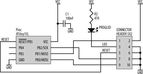
The connector type is an IDC header, and the cable provides all the signals necessary for programming, including one to drive a programming indicator LED. When not being used for programming, the connector may also double as a simple I/O connector for the embedded computer, allowing access to the digital signals. Thus, one piece of hardware can assume dual roles.
There is something important to note, however. If you use PB0, PB1, or PB2 to interface to other components within your computer, care must be taken that the activity of programming does not adversely affect them. For example, our circuit with the MAX4626 used PB2 as the control input. During programming, PB2 acts as SCK, a clock signal. Therefore, the MAX4626 would be rapidly turning on and off as code was downloaded to the processor. If the MAX4626 was controlling something, that device would also rapidly turn on and off, with potentially disastrous effects. Conversely, if there are other components in your system, these must not attempt to drive a signal onto PB0, PB1, or PB2 during the programming sequence. To do so would, at the very least, result in a failed download and, at worst, damage both the embedded system and the programmer. It’s therefore vitally important to consider the implications of in-circuit programming on other components within the system.
So, what’s the answer? Well, we could use PB3 to control the MAX4626 instead, since it doesn’t take part in the programming process. Alternatively, if we needed to use PB2, we could provide a buffer between the processor and the MAX4626, perhaps controlled by ![]() . When
. When ![]() is low (during programming), the buffer is disabled and the MAX4626 is isolated. Another solution may simply be to use a DIP version of the processor, mounted via a socket, and physically remove it for reprogramming. If you’re using a surface-mount version of the processor, perhaps the processor could be mounted on a small PCB that plugs into the embedded computer (much like a memory SIMM on a desktop computer) and may be removed for programming. There are plenty of alternatives, and the best one really depends on your application.
is low (during programming), the buffer is disabled and the MAX4626 is isolated. Another solution may simply be to use a DIP version of the processor, mounted via a socket, and physically remove it for reprogramming. If you’re using a surface-mount version of the processor, perhaps the processor could be mounted on a small PCB that plugs into the embedded computer (much like a memory SIMM on a desktop computer) and may be removed for programming. There are plenty of alternatives, and the best one really depends on your application.
Some AVRs (not the ATtiny15) have the capability of modifying their own program memory with the SPM (Store Program Memory) instruction. With such processors, it is possible for your software to download new code via the processor’s serial port and write this into the program memory. To do so, you need to have your processor preprogrammed with a bootloader program. Normally, you would load all your processors with the bootloader (and Version 1.0 of your application software) during construction. The self-programming can then be used to update the application software when the systems are out in the field. To facilitate this, the program memory is divided into two separate sections: a boot section and an application section. The memory space is divided into pages of either 128 or 256 bytes (depending on the particular processor). Memory must be erased and reprogrammed one page at a time. During programming, the Z register is used as a pointer for the page address, and the r1 and r0 registers together hold the data word to be programmed. The Atmel application note (AVR109: Self-programming), available on its web site, gives sample source code for the bootloader and explains the process in detail.
No matter what processor you are using, the technical data from the chip manufacturer will tell you how to go about putting your code into the processor.
A Bigger AVR
So far, we have looked at a small AVR with very limited capabilities. In later chapters, we will look at various forms of input and output commonly found in embedded systems. For this, we will need processors with more functionality. We have exhausted the ATtiny15, so now we need to move on to processors with a bit more “grunt.” Before getting into the details of I/O in the later chapters, you’ll be introduced to these processors and learn what you need to do to include them in your design.
The first processor is the Atmel AT90S8535 . This is a mid-range AVR with lots of inbuilt I/O, such as a UART, SPI, timers, eight channels of analog input, an analog comparator, and internal EEPROM for parameter storage. The processor has 512 bytes of internal RAM and 8K of flash memory for program storage. Its smaller sibling, the AT90S4434, is identical in every other way except that it has smaller memory spaces of 4K for program storage and 256 bytes of RAM. But from a hardware point of view, the AT90S8535 and the AT90S4434 are the same.
The basic schematic for an AT90S8535-based computer, without any extras, is shown in Figure 15-10. It is not that different from the ATtiny15, save that it has a lot more pins. ![]() has an external pull-up 10k resistor. The processor has an external crystal (X1), and this requires two small decoupling capacitors, C1 and C2. There are four power pins for this processor, and each is decoupled with a 100 nF ceramic capacitor. One of the power inputs (AVCC) is the power supply for the analog section of the chip, and this is isolated from the digital power supply by a 100 Ω resistor, R2. This is to provide a small barrier between the analog section and any switching noise that may be present from the digital circuits. The remaining pins are general-purpose digital I/O, as with the ATtiny15. However, unlike the ATtiny15, these pins have dual functionality. They may be configured, under software control, for alternative I/O functions. The processor’s datasheet gives full details for configuring the functionality of the processor under software control.
has an external pull-up 10k resistor. The processor has an external crystal (X1), and this requires two small decoupling capacitors, C1 and C2. There are four power pins for this processor, and each is decoupled with a 100 nF ceramic capacitor. One of the power inputs (AVCC) is the power supply for the analog section of the chip, and this is isolated from the digital power supply by a 100 Ω resistor, R2. This is to provide a small barrier between the analog section and any switching noise that may be present from the digital circuits. The remaining pins are general-purpose digital I/O, as with the ATtiny15. However, unlike the ATtiny15, these pins have dual functionality. They may be configured, under software control, for alternative I/O functions. The processor’s datasheet gives full details for configuring the functionality of the processor under software control.
This basic AVR design is applicable to most AVRs that you will find. The pinouts may be different, but the basic support required is the same. As with everything, grab the appropriate datasheet, and it will tell you the specifics for the particular processor that you are using.
AVR-Based Datalogger
In the previous chapter, we saw how to design a datalogger based on a PIC16F873A. A datalogger based on an AVR is not too dissimilar. Figure 15-11 shows the basic schematic.
The connections for interfacing a serial dataflash memory chip to an Atmel 90S4434 AVR processor are simply SPI, as with the PIC processor. The AVR portion of the schematic is no different from the examples we have seen previously. That’s the nice thing about simple interfaces such as SPI. They form little subsystem modules that “bolt together” like building blocks. Start with the basic core design and just add peripherals as you need them. The schematic also shows decoupling capacitors for the power supplies, the crystal oscillator for the processor, and a pull-up resistor for ![]() . Pin 41 (PB1) is used as a “manual” (processor-controlled) reset input to the flash.
. Pin 41 (PB1) is used as a “manual” (processor-controlled) reset input to the flash.
The analog inputs, ADC0:ADC7, can be connected to an IDC header allowing for external sampling, or they can be interfaced directly to sensors, as we saw with the PIC datalogger. The serial port signals, RXD and TXD, connect to a MAX3233 in the same way as we saw in the PIC design.

Bus Interfacing
In this section, I’ll show you how to expand the capabilities of your processor by interfacing it to bus-based memories and peripherals. Different processor architectures have different signals and different timing, but once you understand one, the basic principles can be applied to all. Since most small microcontrollers don’t have external buses, the choice is very limited. We’ll look at the one, and only, AVR with an external bus—the AT90S8515. In the PIC world, the PIC17C44 is capable of bus-based interfacing.

AT90S8515 Memory Cycle
A memory cycle (also known as a machine cycle or processor cycle ) is defined as the period of time it takes for a processor to initiate an access to memory (or peripheral), perform the transfer, and terminate the access. The memory cycle generated by a processor is usually of a fixed period of time (or multiples of a given period) and may take several (processor) clock cycles to complete.
Memory cycles usually fall into two categories: the read cycle and the write cycle . The memory or device that is being accessed requires that the data is held valid for a given period after it has been selected and after a read or write cycle has been identified. This places constraints on the system designer. There is a limited amount of time in which any glue logic (interface logic between the processor and other devices) must perform its function, such as selecting which external device is being accessed. The setup times must be met. If they are not, the computer will not function. The glue logic that monitors the address from the processor and uniquely selects a device is known as an address decoder . We’ll take a closer look at address decoders shortly.
Timing is probably the most critical aspect of computer design. For example, if a given processor has a 150 ns cycle time and a memory device requires 120 ns from when it is selected until when it has completed the transfer, this leaves only 30 ns at the start of the cycle in which the glue logic can manipulate the processor signals. A 74LS series TTL gate has a typical propagation delay of 10 ns. So, in this example, an address decoder implemented using any more than two 74LS gates (in sequence) is cutting it very fine.
A synchronous processor has memory cycles of a fixed duration, and all processor timing is directly related to the clock. It is assumed that all devices in the system are capable of being accessed and responding within the set time of the memory cycle. If a device in the system is slower than that allowed by the memory cycle time, logic is required to pause the processor’s access, thus giving the slow device time to respond. Each clock cycle within this pause is known as a wait state. Once sufficient time has elapsed (and the device is ready), the processor is released by the logic and continues with the memory cycle. Pausing the processor for slower devices is known as inserting wait states . The circuitry that causes a processor to hold is known as a wait-state generator . A wait-state generator is easily achieved using a series of flip-flops acting as a simple counter. The generator is enabled by a processor output indicating that a memory cycle is beginning and is normally reset at the end of the memory cycle to return it to a known state. (Some processors come with internal, programmable wait-state generators.)
An asynchronous processor (such as a 68000) does not terminate its memory cycle within a given number of clock cycles. Instead, it waits for a transfer acknowledge assertion from the device or support logic to indicate that the device being accessed has had sufficient time to complete its part in the memory cycle. In other words, the processor automatically inserts wait states in its memory cycle until the device being accessed is ready. If the processor does not receive an acknowledge, it will wait indefinitely. Many computer systems using asynchronous processors have additional logic to cause the processor to restart if it waits too long for a memory cycle to terminate. An asynchronous processor can be made into a synchronous processor by tying the acknowledge line to its active state. It then assumes that all devices are capable of keeping up with it. This is known as running with no wait states.
Most microcontrollers are synchronous, whereas most larger processors are asynchronous. The AT90S8515 is a synchronous processor, and it has an internal wait-state generator capable of inserting a single wait state.
Bus Signals
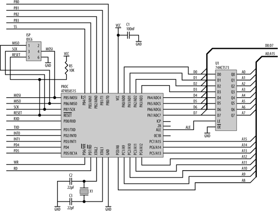
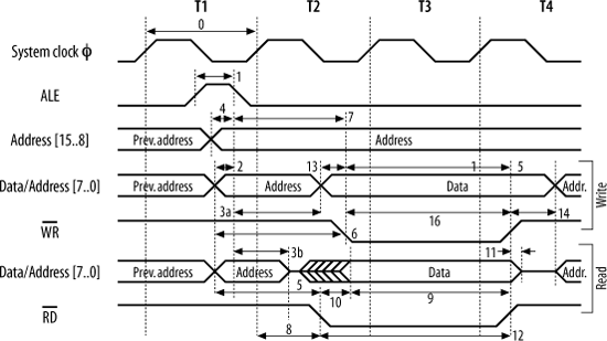
Figure 15-12 shows an AT90S8515 processor with minimal support components. The AT90S8515 has an address bus, a data bus, and a control bus that it brings to the outside world for interfacing. Since this processor has a limited number of pins, these buses share pins with the digital I/O ports (“port A” and “port C”) of the processor. A bit in a control register determines whether these pins are I/O or bus pins. Now, a 16-bit address bus and an 8-bit data bus add up to 24 bits, but ports A and B have only 16 bits between them. So how does the processor fit 24 bits into 16? It multiplexes the lower half of the address bus with the data bus. At the start of a memory access, port A outputs address bits A0:A7. The processor provides a control line, ALE (Address Latch Enable), which is used to control a latch, such as a 74HCT573 (shown on the right in Figure 15-12). As ALE falls, the latch grabs and holds the lower address bits. At the same time, port B outputs the upper address bits, A8:A15. These are valid for the entire duration of the memory access. Once the latch has acquired the lower address bits, port A then becomes the data bus for information transfer between the processor and an external device. Also shown in Figure 15-12 are the crystal circuit, the In-System Programming port, decoupling capacitors for the processor’s power supply, and net labels for other important signals.
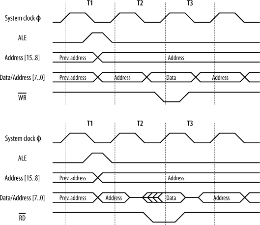
The timing diagrams for an AT90S8515 are shown in Figure 15-13. The cycle “T3” exists only when the processor’s wait-state generator is enabled.
Now, let’s look at these signals in more detail. (We’ll see later how you actually work with this information. For the moment, we’re just going to “take a tour” of the timing diagrams.) The numbers for the timing information can be found in the datasheet, available from Atmel’s web site. Figure 15-14 shows the timing information as presented in the Atmel datasheet, complete with timing references.
The references are looked up in the appropriate table in the processor’s datasheet (Table 15-2).
|
8 MHz oscillator |
Variable oscillator | ||||||
|
Ref. # |
Symbol |
Parameter |
Min |
Max |
Min |
Max |
Unit |
|
0 |
1/tCLCL |
Oscillator Frequency |
0.0 |
8.0 |
MHz | ||
|
1 |
tLHLL |
ALE Pulse Width |
32.5 |
0.5 tCLCL- 30.0 |
ns | ||
|
2 |
tAVLL |
Address Valid A to ALE Low |
22.5 |
0.5 tCLCL- 40.0 |
ns | ||
|
3a |
tLLAX...ST |
Address Hold after ALE Low, ST/STD/STS Instructions |
67.5 |
0.5 tCLCL+5.0 |
ns | ||
|
3b |
tLLAX...LD |
Address Hold after ALE Low, LD/LDD/LDS Instructions |
15.0 |
15.0 |
ns | ||
|
4 |
tAVLLC |
Address Valid C to ALE Low |
22.5 |
0.5 tCLCL- 40.0 |
ns | ||
|
5 |
tAVRL |
Address Valid to RD Low |
95.0 |
1.0 tCLCL- 30.0 |
ns | ||
|
6 |
tAVWL |
Address Valid to WR Low |
157.5 |
1.5 tCLCL- 30.0 |
ns | ||
|
7 |
tLLWL |
ALE Low to WR Low |
105.0 |
145.0 |
1.0 tCLCL- 20.0 |
1.0 tCLCL+ 20.0 |
ns |
|
8 |
tLLRL |
ALE Low to RD Low |
42.5 |
82.5 |
0.5 tCLCL- 20.0 |
0.5 tCLCL+ 20.0 |
ns |
|
9 |
tDVRH |
Data Setup to RD High |
60.0 |
60.0 |
ns | ||
|
10 |
tRLDV |
Read Low to Data Valid |
70.0 |
1.0 tCLCL- 55.0 |
ns | ||
|
11 |
tRHDX |
Data Hold after RD High |
0.0 |
0.0 |
ns | ||
|
12 |
tRLRH |
RD Pulse Width |
105.0 |
1.0 tCLCL- 20.0 |
ns | ||
|
13 |
tDVWL |
Data Setup to WR Low |
27.5 |
0.5 tCLCL- 35.0 |
ns | ||
|
14 |
tWHDX |
Data Hold after WR High |
0.0 |
0.0 |
ns | ||
|
15 |
tDVWH |
Data Valid to WR High |
95.0 |
1.0 tCLCL- 30.0 |
ns | ||
|
16 |
tWLWH |
WR Pulse Width |
42.5 |
0.5 tCLCL- 20.0 |
ns | ||
The system clock is shown at the top of both diagrams for reference, since all processor activity relates to this clock. The period of the clock is designated in the Atmel datasheet as “tCLCL"[*] and is equal to 1/frequency. For an 8 MHz clock, this is 125 ns. The width of T1, T2, and T3 are each tCLCL.
No processor cycle exists in isolation. There is always[†] a preceding cycle and following cycle. We can see this in the timing diagrams. At the start of the cycles, the address from the previous access is still present on the address bus. On the falling edge of the clock, in cycle T1, the address bus changes to become the valid address required for this cycle. Port A presents address bits A0:A7, and port B presents A8:A15. At the same time, ALE goes high, releasing the external address latch in preparation for acquiring the new address from port A. ALE stays high for 0.5 x tCLCL - 30 ns. So, for example, with an AT90S8515 running at 8 MHz, ALE stays high for 32.5 ns. ALE falls, causing the external latch to acquire and hold the lower address bits. Prior to ALE falling, the address bits will have been valid for 0.5 x tCLCL - 40 ns or, in other words, 40 ns before the system clock rises at the end of the T1 period. After ALE falls, the lower address bits will be held on port A for 0.5 x tCLCL + 5 ns for a write cycle before changing to data bits. For a read cycle, they are held for a minimum of 15 ns only. The reason this is so much shorter for a read cycle is that the processor wishes to free those signal pins as soon as possible. Since this is a read cycle, an external device is about to respond, which means the processor needs to “get out of the way” as soon as it can.
For a write cycle, tCLCL - 20 ns after ALE goes low, the write strobe, ![]() , goes low. This indicates to external devices that the processor has output valid data on the data bus.
, goes low. This indicates to external devices that the processor has output valid data on the data bus. ![]() will be low for
will be low for 0.5 x tCLCL - 20 ns. This time allows the external device to prepare to read in (latch) the data. On the rising edge of ![]() , the external device is expected to latch the data presented on the data bus. At this point, the cycle completes, and the next cycle is about to begin.
, the external device is expected to latch the data presented on the data bus. At this point, the cycle completes, and the next cycle is about to begin.
For a read cycle, the read strobe, ![]() , goes low
, goes low 0.5 x tCLCL - 20 ns after ALE is low. ![]() will be low for
will be low for tCLCL - 20 ns. During this time, the external device is expected to drive valid data onto the data bus. It can present data anytime after ![]() goes low, so long as data is present and stable at least 60 ns before
goes low, so long as data is present and stable at least 60 ns before ![]() goes high again. At this point, the processor latches the data from the external device, and the read cycle terminates. Note that many processors do not have a separate read-enable signal, so this must be generated by external logic, based on the premise that if the cycle is not a write cycle, it must be a read cycle.
goes high again. At this point, the processor latches the data from the external device, and the read cycle terminates. Note that many processors do not have a separate read-enable signal, so this must be generated by external logic, based on the premise that if the cycle is not a write cycle, it must be a read cycle.
So, that is how an AT90S8515 expects to access any external device attached to its buses, whether those devices are memory chips or peripherals. But how does it work in practice? Let’s look at designing[*] a computer based on an AT90S8515 with some external devices. For this example, we will interface the processor to a static RAM and some simple latches that we could use to drive banks of LEDs.
Memory Maps and Address Decoding
To the processor, its address space is one big, linear region. Although there may be numerous devices within that space, both internal to the processor and external, it makes no distinction between devices. The processor simply performs memory accesses in the address space. It is up to the system designer (that’s you) to allocate regions of memory to each device and then provide address-decode logic. The address decoder takes the address provided by the processor during an external access and uniquely selects the appropriate device (Figure 15-15). For example, if we have a RAM occupying a region of memory, any address from the processor corresponding to within that region should select the RAM and not select any other device. Similarly, any address outside that region should leave the RAM unselected.
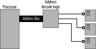
The allocation of devices within an address space is known as a memory map
or address map
. The address spaces for an AT90S8515 processor are shown in Figure 15-16. Any device we interface to the processor must be within the data memory space. Thus, we can ignore the processor’s internal program memory. As the processor has Harvard architecture, the program space is a completely separate address space. Within the 64K data space lie the processor’s internal resources: the working registers, the I/O registers, and the internal 512 bytes of SRAM. These occupy the lowest addresses within the space. Any address above 0x0260 is ours to play with. (Not all processors have resources that are memory-mapped, and, in those cases, the entire memory space is usable by external devices.)
Now, our first task is to allocate the remaining space to the external devices. Since the RAM is 32K in size, it makes sense to place it within the upper half of the address space (0x8000-0xFFFF). Address decoding becomes much easier if devices are placed on neat boundaries. Placing the RAM between addresses 0x8000 and 0xFFFF leaves the lower half of the address space to be allocated to the latches and the processor’s internal resources. Now a latch need only occupy a single byte of memory within the address space. So, if we have three latches, we need only three bytes of the address space to be allocated. This is known as explicit address decoding. However, there’s a good reason not to be so efficient with our address allocation. Decoding the address

down to three bytes would require an address decoder to use 14 bits of the address. That’s a lot of (unnecessary) logic to select just three devices. A better way is simply to divide the remaining address space into four, allocating three regions for the latches and leaving the fourth unused (for the processor’s internal resources). This is known as partial address decoding and is much more efficient. The trick is to use the minimal amount of address information to decode for your devices.
Our address map allocated to our static RAM and three latches is shown in Figure 15-17. Note that the lowest region leaves the addresses in the range 0x0260 to 0x1FFF unused.

Any address within the region 0x2000 to 0x3FFF will select Latch0, even though that latch needs only one byte of space. Thus, the device is said to be mirrored within that space. For simplicity in programming, you normally just choose an address (0x2000 say) and use that within your code. But you could just as easily use address 0x290F, and that would work too.
We now have our memory map, and we need to design an address decoder. We start by tabling the devices along with their addresses (Table 15-3). We need to look for which address bits are different between the devices, and which address bits are common within a given device’s region.
|
Device |
Address range |
A15 .. A0 |
|
Unused |
0x0000-0x1FFF |
0000 0000 0000 0000 0000 0001 1111 1111 1111 1111 |
|
Latch0 |
0x2000-0x3FFF |
0010 0000 0000 0000 0000 0011 1111 1111 1111 1111 |
|
Latch1 |
0x4000-0x5FFF |
0100 0000 0000 0000 0000 0101 1111 1111 1111 1111 |
|
Latch2 |
0x6000-0x7FFF |
0110 0000 0000 0000 0000 0111 1111 1111 1111 1111 |
|
RAM |
0x8000-0xFFFF |
1000 0000 0000 0000 0000 1111 1111 1111 1111 1111 |
So, what constitutes a unique address combination for each device? Looking at the table, we can see that for the RAM, address bit (and address signal) A15 is high, while for every other device it is low. We can therefore use A15 as the trigger to select the RAM. For the latches, address bits A15, A14, and A13 are critical. So we can redraw our table to make it clearer. This is the more common way of doing an address table, as shown in Table 15-4. An “x” means a “don’t care” bit.
|
Device |
Address range |
A15 .. A0 |
|
Unused |
0x0000-0x1FFF |
000x xxxx xxxx xxxx xxxx |
|
Latch0 |
0x2000-0x3FFF |
001x xxxx xxxx xxxx xxxx |
|
Latch1 |
0x4000-0x5FFF |
010x xxxx xxxx xxxx xxxx |
|
Latch2 |
0x6000-0x7FFF |
011x xxxx xxxx xxxx xxxx |
|
RAM |
0x8000-0xFFFF |
1xxx xxxx xxxx xxxx xxxx |
Therefore, to decode the address for the RAM, we simply need to use A15. If A15 is high, the RAM is selected. If A15 is low, then one of the other devices is selected and the RAM is not. Now, the RAM has a chip select (![]() ) that is active low. So when A15 is high,
) that is active low. So when A15 is high, ![]() should go low. So, our address decoder for the RAM is simply to invert A15 using an inverter chip such as a 74HCT04 (Figure 15-18). It is common practice to label the chip-select signal after the device it is selecting. Hence, our chip select to the RAM is labeled
should go low. So, our address decoder for the RAM is simply to invert A15 using an inverter chip such as a 74HCT04 (Figure 15-18). It is common practice to label the chip-select signal after the device it is selecting. Hence, our chip select to the RAM is labeled ![]() .
.

Note that for the RAM to respond, it needs both a chip select and either a read or write strobe from the processor. All other address lines from the processor are connected directly to the corresponding address inputs of the RAM (Figure 15-19).

Now for the other four regions, A15 must be low, and A14 and A13 are sufficient to distinguish between the devices. Having our address decoder use discrete logic would require several gates and would be “messy.” There’s a simpler way. We can use a 74HCT139 [*] decoder, which takes two address inputs (A and B) and gives us four unique, active-low, chip-select outputs (labeled Y0:Y3). Since the latches require active-high enables, we use inverters on the outputs of the 7HCT139. So our complete address decoder for the computer is shown in Figure 15-20.
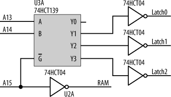
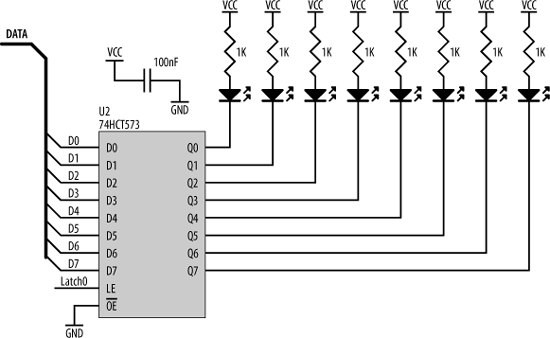
The 74HCT139 uses A15 (low) as an enable (input ![]() ), and, in this way, A15 is included as part of the address decode. If we needed to decode for eight regions instead of four, we could have used a 74HCT138 decoder, which takes three address inputs and gives us eight chip selects. The interface between the processor and an output latch is simple. We can use the same type of latch (a 74HCT573) that we used to demultiplex the address. Such an output latch could be used in any situation in which we need some extra digital outputs. In the sample circuit shown in Figure 15-21, I’m using the latch to control a bank of eight LEDs.
), and, in this way, A15 is included as part of the address decode. If we needed to decode for eight regions instead of four, we could have used a 74HCT138 decoder, which takes three address inputs and gives us eight chip selects. The interface between the processor and an output latch is simple. We can use the same type of latch (a 74HCT573) that we used to demultiplex the address. Such an output latch could be used in any situation in which we need some extra digital outputs. In the sample circuit shown in Figure 15-21, I’m using the latch to control a bank of eight LEDs.
The output from our 74HCT139 address decoder is used to drive the LE (Latch Enable) input of the 74HCT573. Whenever the processor accesses the region of memory space allocated to this device, the address decoder triggers the latch to acquire whatever is on the data bus. And so, the processor simply writes a byte to any address in this latch’s address region, and that byte is acquired and output to the LEDs. (Writing a “0” to a given bit location will turn on a LED; writing a “1” will turn it off.)
Note that the latch’s output enable (![]() ) is permanently tied to ground. This means that the latch is always displaying the byte that was last written to it. This is important, as we always want the LEDs to display, and not just transitorily blink on, while the processor is accessing them.
) is permanently tied to ground. This means that the latch is always displaying the byte that was last written to it. This is important, as we always want the LEDs to display, and not just transitorily blink on, while the processor is accessing them.
Using the 74HCT139 in preference to discrete logic gates makes our design much simpler, but there’s an even better way to implement system glue.
PALs
It is now rare to see support logic implemented using individual gates. It is more common to use programmable logic (PALs, LCAs, or PLDs)[*] to implement the miscellaneous “glue” functions that a computer system requires. Such devices are fast, take up relatively little space, have low power consumption, and, as they are reprogrammable, make system design much easier and more versatile.
There is a wide range of devices available, from simple chips that can be used to implement glue logic (just as we are about to do) to massive devices with hundreds of thousands of gates. Altera (http://www.altera.com), Xilinx (http://www.xilinx.com), Lattice Semiconductor (http://www.latticesemi.com), and Atmel are some manufacturers to investigate for large-scale programmable logic. These big chips are sophisticated enough to contain entire computer systems. Soft cores are processor designs implemented in gates, suitable for incorporating into these logic devices. You can also get serial interfaces, disk controllers, network interfaces, and a range of other peripherals, all for integration into one of these massive devices. Of course, it’s also fun to experiment and design your own processor from the ground up.
Each chip family requires its own suite of development tools. These allow you to create your design (either using schematics or some programming language such as VHDL), simulate the system, and finally download your creation into the chip. You can even get C compilers for these chips that will take an algorithm and convert it, not into machine code, but into gates. What was software now runs not on hardware, but as hardware. Sounds cool, but the tools required to play with this stuff can be expensive. If you just want to throw together a small, embedded system, they are probably out of your price range. For what we need to do for our glue logic, such chips are overkill. Since our required logic is simple, we will use a simple (and cheap) PAL that can be programmed using freely available, public-domain software.
PALs are configured using equations to represent the internal logic. “+” represents OR, “*” represents AND, and “/” represents NOT. (These symbols are the original operator symbols that were used in Boolean logic. If you come from a programming background, these symbols may seem strange to you. You will be used to seeing “|”, “&”, and “!”.) The equations are compiled using software such as PALASM, ABEL, or CUPL to produce a JED file. This is used by a device known as a PAL burner to configure the PAL. In many cases, standard EPROM burners will also program PALs.
PALs have pins for input, pins for output, and pins that can be configured as either input or output. Most of the PAL’s pins are available for your use. In your PAL source code file (PDS file), you declare which pins you are using and label them. This is not unlike declaring variables in program source code, except that instead of allocating bytes of RAM, you’re allocating physical pins of a chip. You then use those pin labels within equations to specify the internal logic. Our address decoder, implemented in a PAL, would have the following equations to specify the decode logic:
RAM = /A15
LATCH0 = (/A15 * /A14 * A13)
LATCH1 = (/A15 * A14 * /A13)
LATCH2 = (/A15 * A14 * A13)
I have (deliberately) written the above equations in a form that makes it easier to compare them with the address tables listed previously. You could simplify these equations, but there is no need. Just as an optimizing C compiler will simplify (and speed up) your program code, so too will PALASM rework your equations to optimize them for a PAL.
A PDS file to program a 22V10 PAL for the above address decode might look something like:
TITLE decoder.pds          ; name of this file
PATTERN
REVISION 1.0
AUTHOR John Catsoulis
DATE January 2005

CHIP decoder PAL22V10      ; specify which PAL device you
                           ; are using and give it a name ("decoder")

PIN   2   A15              ; pin declarations and allocations
PIN   3   A14
PIN   12  LATCH0
PIN   13  LATCH1
PIN   14  LATCH2
PIN   15  RAM

EQUATIONS                  ; equations start here

RAM = /A15
LATCH0 = (/A15 * /A14 * A13)
LATCH1 = (/A15 * A14 * /A13)
LATCH2 = (/A15 * A14 * A13)
The advantages of using a PAL for system logic are twofold. The PAL equations may be changed to correct for bugs or design changes. The propagation delays through the PAL are of a fixed and small duration (no matter what the equations), which makes analyzing the overall system’s timing far simpler. For very simple designs, it probably doesn’t make a lot of difference whether you use PALs or individual chips. However, for more complicated designs, programmable logic is the only option. If you can use programmable logic devices instead of discrete logic chips, please do so. They make life much easier.
Timing Analysis
Now that we have finished our logic design, the question is: will it actually work? It’s time (pardon the pun) to work through the numbers and analyze the timing. This is the least fun, and most important, part of designing a computer.
We start with the signals (and timing) of the processor, add in the effects of our glue logic, and finally see if this falls within the requirements of the device to which we are interfacing. We’ll work through the example for the SRAM. For the other devices, the analysis follows the same method. The timing diagram for a read cycle for the SRAM is shown in Figure 15-22. The RAM I have chosen is a CY62256-70 (32K) SRAM made by Cypress Semiconductor. Most 32K SRAMs follow the JEDEC standard, which means their pinouts and signals are all compatible. So, what works for one 32K SRAM should work for them all. But the emphasis is on should, and, as always, check the datasheet for the individual device you are using.
The “-70” in the part number means that this is a “70 ns SRAM,” or, put simply, the access time for the chip is 70 ns. Now, from the CY62256-70 datasheet (available from http://www.cypress.com), tRC is a minimum of 70 ns. This means that the chip enable, ![]() , can be low for no less than 70 ns.
, can be low for no less than 70 ns. ![]() is just our chip select (
is just our chip select (![]() ) from our address decoder, so we need to ensure that the address decoder will hold
) from our address decoder, so we need to ensure that the address decoder will hold ![]() low for at least this amount of time. For the SRAM to output data during a read cycle, it needs a valid address, an active chip enable, and an active output enable (
low for at least this amount of time. For the SRAM to output data during a read cycle, it needs a valid address, an active chip enable, and an active output enable (![]() ). The output enable is just the read strobe (
). The output enable is just the read strobe (![]() ) from the processor. These three conditions must be met before the chip will respond with data. It will take 70 ns
) from the processor. These three conditions must be met before the chip will respond with data. It will take 70 ns
from ![]() low (tACE) or 35 ns from
low (tACE) or 35 ns from ![]() low (tDOE), whichever is the latter, until data is output. Now,
low (tDOE), whichever is the latter, until data is output. Now, ![]() is generated by our address decoder (which in turn uses address information from the processor), and
is generated by our address decoder (which in turn uses address information from the processor), and ![]() (
(![]() ) comes from the processor. During a read cycle, the processor will output a read strobe and an address, which in turn will trigger the address decoder. Some time later in the cycle, the processor will expect data from the RAM to be present on the data bus. It is critical that the signals that cause the RAM to output data will do so such that there will be valid data when the processor expects it. Meet this requirement, and you have a processor that can read from external memory. Fail this requirement, and you’ll have an intriguing paperweight and a talking piece at parties.
) comes from the processor. During a read cycle, the processor will output a read strobe and an address, which in turn will trigger the address decoder. Some time later in the cycle, the processor will expect data from the RAM to be present on the data bus. It is critical that the signals that cause the RAM to output data will do so such that there will be valid data when the processor expects it. Meet this requirement, and you have a processor that can read from external memory. Fail this requirement, and you’ll have an intriguing paperweight and a talking piece at parties.
We start with the processor. I’m assuming that the processor’s wait-state generator is disabled. For an AT90S8515 processor, everything is referenced to the falling edge of ALE . The high-order address bits, which feed our address decoder, become valid 22.5 ns prior to ALE going low on an 8 MHz AT90S8515. If we’re using a 74HCT139 as an address decoder,[*] this takes 40 ns to respond to a change in inputs. So, our chip select for the RAM will become valid 17.5 ns after ALE has fallen (Figure 15-23).
Now, ![]() will go low between 42.5 ns and 82.5 ns after ALE falls. Since the RAM will not output data until
will go low between 42.5 ns and 82.5 ns after ALE falls. Since the RAM will not output data until ![]() (
(![]() ) is low, we take the worst case of 82.5 ns (Figure 15-24).
) is low, we take the worst case of 82.5 ns (Figure 15-24).
The RAM will respond 70 ns after ![]() and 35 ns after
and 35 ns after ![]() , whichever comes last. So, 70 ns from
, whichever comes last. So, 70 ns from ![]() low is 87.5 ns after ALE, and 35 ns after
low is 87.5 ns after ALE, and 35 ns after ![]() is 117.5 ns after ALE. Therefore,
is 117.5 ns after ALE. Therefore, ![]() is the determining control signal in this case. This means that the SRAM will output valid data 117.5 ns after ALE falls (Figure 15-25).
is the determining control signal in this case. This means that the SRAM will output valid data 117.5 ns after ALE falls (Figure 15-25).
Now, an 8 MHz processor expects to latch valid data during a read cycle at 147.5 ns after ALE. So our SRAM will have valid data ready with 30 ns to spare. So far, so good. But what about at the end of the cycle? Now, the processor expects the data bus to be released and available for the next access at 200 ns after ALE falls. The RAM takes 25 ns from when it is released by ![]() until it stops outputting data onto the data bus. This means that the data bus will be released by the RAM at 142.5 ns. So that will work too.
until it stops outputting data onto the data bus. This means that the data bus will be released by the RAM at 142.5 ns. So that will work too.
The analysis for a write cycle is done in a similar manner. It is important to do this type of analysis for every device interfaced to your processor, for every type of memory cycle. It can be difficult, because datasheets are notorious for leaving out information or presenting necessary data in a roundabout way. Working through it all can be time-consuming and frustrating, and it’s far too easy to make a mistake. However, it is very necessary. Without it, you’re relying on blind luck to make your computers run, and that’s not good engineering.
Memory Management
In most small-scale embedded applications, the connections between a processor and an external memory chip are straightforward. Sometimes, though, it’s advantageous to play with the natural order of things. This is the realm of memory management.
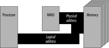
Memory management deals with the translation of logical addresses to physical addresses and vice versa. A logical address is the address output by the processor. A physical address is the actual address being accessed in memory. In small computer systems, these are often the same. In other words, no address translation takes place, as illustrated in Figure 15-26.

For small computer systems, this absence of memory management is satisfactory. However, in systems that are more complex, some form of memory management may become necessary. There are four cases where this might be so:
- Physical memory > logical memory
When the logical address space of the processor (determined by the number of address lines) is smaller than the actual physical memory attached to the system, it becomes necessary to map the logical space of the processor into the physical memory space of the system. This is sometimes known as banked memory . This is not as strange or uncommon as it may sound. Often, it is necessary to choose a particular processor for a given attribute, yet that processor may have a limited address space—too small for the application. By implementing banked memory, the address space of the processor is expanded beyond the limitation of the logical address range.
- Logical memory > physical memory
When the logical address space of the processor is very large, it is not always practical to fill this address space with physical memory. It is possible to use some space on disk as virtual memory , thus making it appear that the processor has more physical memory than exists within the chips. Memory management is used to identify whether a memory access is to physical memory or virtual memory and must be capable of swapping the virtual memory on disk with real memory and performing the appropriate address translation.
- Memory protection
It is often desirable to prevent some programs from accessing certain sections of memory. Protection can prevent a crashing program from corrupting the operating system and bringing down the computer. It is also a way of channeling all I/O access via the operating system, since protection can be used to prevent all software (save the OS) from accessing the I/O space.
- Task isolation
In a multitasking system, tasks should not be able to corrupt each other (by stomping on each other’s memory space, for example). In addition, two separate tasks should be able to use the same logical address in memory, with memory management performing the translation to separate, physical addresses.
The basic idea behind memory management is quite simple, but the implementation can be complicated, and there are nearly as many memory-management techniques as there are computer systems that employ memory management. Memory management is performed by a Memory Management Unit (MMU ). The basic form of this is shown in Figure 15-27. An MMU may be a commercial chip, a custom-designed chip (or logic), or an integrated module within the processor. Most modern, fast processors incorporate MMUs on the same chip as the CPU.

Page mapping
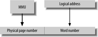
In all practical memory-management systems, words of memory are grouped together to form pages, and an address can be considered to consist of a page number and the number of a word within that page. The MMU translates the logical page to a physical page, while the word number is left unchanged (Figure 15-28). In practice, the overall address is just a concatenation of the page number and the word number.

The logical address from the processor is divided into a page number and a word number. The page number is translated by the MMU and recombined with the word number to form the physical address presented to memory (Figure 15-29).

Banked memory
The simplest form of memory management is when the logical address space is smaller than the physical address space. If the system is designed such that the size of a page is equal to the logical address space, then the MMU provides the page number, thus mapping the logical address into the physical address (Figure 15-30).
The effective address space from this implementation is shown in Figure 15-31. The logical address space can be mapped (and remapped) to anywhere in the physical address space.

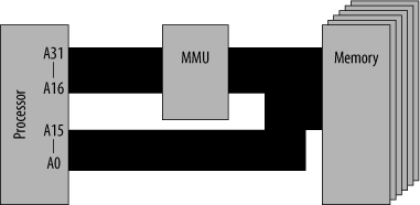
The system configuration for this is shown in Figure 15-32. This technique is often used in processors with 16-bit addresses (64K logical space) to give them access to larger memory spaces.
For many small systems, banked memory may be implemented simply by latching (acquiring and holding) the data bus and using this as the additional address bits for the physical memory (Figure 15-33). The latch appears in the processor’s logical space as just another I/O device. To select the appropriate bank of memory, the processor stores the bank bits to the latch, where they are held. All subsequent memory accesses in the logical address space take place within the selected bank. In this example, the processor’s address space acts as a 64K window into the larger RAM chip. As you can see, while memory management may seem complex, its actual implementation can be quite simple.

Tip
This technique has also been used in desktop systems. The old Apple /// computer came with up to 256K of memory, yet the address space of its 6502 processor was only 64K.
Figure 15-34 shows the actual wiring required for a banked-memory implementation for our AT90S8515 AVR system, replacing the 32K RAM with a 512K RAM.
The RAM used is an HM628511H made by Hitachi. In this implementation, we still have the RAM allocated into the upper 32K of the processor’s address space as before. In other words, the upper 32K of the processor’s address space is a window into the 512K RAM. The lower 32K of the processor’s address space is used for I/O devices, as before. Address bits A0 to A14 connect to the RAM as before, and the data bus (D0 to D7) connects to the data pins (IO1 to IO8 [*]) of the SRAM.
Now, we also have a 74HCT573 latch, which is mapped into the processor’s address space, just as we did with the LEDs latch. The processor can write to this latch, and it will hold the written data on its outputs. The lower nybble of this latch is used to provide the high-order address bits for the RAM.
Let’s say the processor wants to access address 0x1C000. In binary, this is %001 1100 0000 0000 0000. The lower 15 address bits (A0 to A14) are provided directly by the processor. The remaining address bits must be latched. So, the processor first stores the byte 0x03 to the latch, and the RAM’s address pins A18, A17, A16, and A15 see
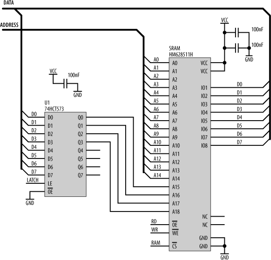
%0011 (0x03), respectively. That region of the RAM is now banked to the processor’s 32K window. When the processor accesses address 0xC000, the high-order address bit (A15) from the processor is used by the address decoder to select the RAM by sending its ![]() input low. The remaining 15 address bits (A0 to A14) combine with the outputs of the latch to select address
input low. The remaining 15 address bits (A0 to A14) combine with the outputs of the latch to select address 0x1C000.
The NC pins are “No Connection” and are left unwired.
Address translation
For processors with larger address spaces, the MMU can provide translation of the upper part of the address bus (Figure 15-35).
The MMU contains a translation table , which remaps the input addresses to different output addresses. To change the translation table, the processor must be able to access the MMU. (There is little point in having an MMU if the translation table is unalterable.) Some processors are specifically designed to work with an MMU, while
other processors have MMUs incorporated. However, if the processor being used was not designed for use with an MMU, it will have no special support. The processor must therefore communicate with the MMU as though it were any other peripheral device using standard read/write cycles. This means the MMU must appear in the processor’s address. It may seem that the simplest solution is to map the MMU into the physical address space of the system. In real terms, this is not practical. If the MMU is ever (intentionally or accidentally) mapped out of the current logical address space (such that the physical page on which the MMU is located is not part of the current logical address space), it becomes impossible to access the MMU ever again. This may also happen when the system powers up, because the contents of the MMU’s translation table may be unknown.
The solution is to decode the chip select for the MMU directly from the logical address bus of the processor. Hence, the MMU will lie at a constant address in the logical space. This removes the possibility of “losing” the MMU, but it introduces another problem. Since the MMU now lies directly in the logical address space, it is no longer protected from accidental tampering (by a crashing program) or illegal and deliberate tampering in a multitasking system. To solve this problem, many larger processors have two states of operation--supervisor state and user state --with separate stack pointers for each mode. This provides a barrier between the operating system (and its privileges) and the other tasks running on the system. The state the processor is in is made available to the MMU through special status pins on the processor. The MMU may be modified only when the processor is in supervisor state, thereby preventing modification by user programs. The MMU uses a different logical-to-physical translation table for each state. The supervisor translation table is usually configured on system initialization, then remains unchanged. User tasks (user programs) normally run in user state, whereas the operating system (which performs task swapping and handles I/O) runs in supervisor state. Interrupts also place the processor in supervisor state, so that the vector table and service routines do not have to be part of the user’s logical address space. While in user state, tasks may be denied access to particular pages of physical memory by the operating system.
[*] Datasheet nomenclature can often be very cryptic. The “CL” comes from “clock.” Since Atmel is using four-character subscripts for its timing references, it pads by putting “CL” twice. You don’t really need to know what the subscripts actually mean; you just need to know the signals they refer to and the actual numbers involved.
[†] I’m ignoring coming out of reset, or just before power-off!
[*] Since we’ve covered oscillators and in-circuit programming previously, I’ll ignore those in this discussion. That doesn’t mean you should leave them out of your design!
[*] There are actually two separate decoders in each 74HCT139 chip. We’ll need only one.
[*] Programmable Array Logic, Logic Cell Arrays, and Programmable Logic Devices, respectively.
[*] PALs may respond in 15 ns or less. This is another reason why PALs are a better choice than discrete logic.
[*] Memory chip manufacturers often label data pins as “IO” pins, since they perform data input and output for the device.