
Chapter 14. The PIC Microcontrollers
Where a calculator on the ENIAC is equipped with 18,000 vacuum tubes and weighs 30 tons, computers in the future may have only 1,000 vacuum tubes and perhaps weigh 1 ½ tons.
— Popular Mechanics, March 1949
This chapter introduces you to the Microchip PIC. To start our discussion of microprocessor hardware, we’ll look at the basics of creating computer hardware by designing a small computer based on a simple 8-pin PIC processor. The same design principles apply to the AVR and many other microcontrollers. This PIC processor is so simple that building a computer based on one of them is trivial, as you will see. From there, we’ll look at a mid-range PIC processor and see just what you need to do to design an embedded computer based on one. First, though, let’s take a quick tour of the PIC architectures before getting into designing some computers.
A Tale of Two Processors
In the late 1970s, General Instruments had a 16-bit processor known as the CP1600. It has since passed into extinction and is all but forgotten, long ago losing out to the Intel 8086 and the Motorola 68000. One major failing of the CP1600 was that it had limited I/O capability, and so General Instruments designed a tiny companion processor to act as an I/O controller. The idea was that this controller could provide not only the I/O for the CP1600, but being a processor in its own right, it could provide some degree of intelligent control. This processor was called the Peripheral Interface Controller, or PIC. The CP1600 died a quiet death, passing gently into oblivion, but its little companion lives on. In the mid-80s, the microelectronics division of General Instruments was spun off into Microchip, and the PIC processor was its core product. Today, PICs are widely used. They live in the hand controllers of Sony PlayStations, children’s toys, consumer appliances, and industrial systems.
The original PIC architecture has only one accumulator (known as the working register , or w register) and 25 to 368 bytes of RAM in the original processors. The program counter’s least significant byte, the status register, and various control registers are mapped into the lowest part of the RAM space and may be accessed by standard memory move operations. The upper part of the RAM space is for data. Microchip refers to the RAM space as “registers,” although they have limited functionality as true registers. They are primarily for data storage.
The processor has a stack that is fixed to a depth of between two and eight entries (depending on the particular processor) and is used solely for holding return addresses for subroutine calls and interrupts. There is a single register, known as the FSR ( File Select Register ), which can act as an index register into the RAM space. Limited indexed addressing is available using the FSR, and it can be used to implement a pseudostack for user data.
Apart from a few exceptions, the PIC has no external buses and is a self-contained computer within a single chip. Only limited expansion is possible using the processor’s peripheral interfaces (SPI and I2C) or digital I/O ports. The PIC excels in applications for which size and power consumption are critical. Being able to drop a tiny computer system into a design is a great bonus, and it is ideal for battery-powered applications, since it can (almost) run off the field of a stray electron.
The PIC is also very robust. It takes a lot to kill a PIC. I had one client that inadvertently switched power and ground on his PIC-based computer and left it that way for a week. At the end of it, the little processor was still operational (once powered the right way). Another time, one of my PIC-based dataloggers was tested for its long endurance by attaching it to the Indian Pacific express. This is a long-haul passenger train that goes between Sydney and Perth, crossing the deserts of central Australia. Unfortunately, during the trial the Indian Pacific was involved in a serious rail accident. A signaling fault caused a commuter train to impact the rear of the express, completely demolishing the end carriages. The datalogger had been attached (externally) to the rear of the train. It absorbed the full impact of the collision, and, when recovered from the wreckage, the datalogger was still operating normally. PICs are tough little processors!
The PIC is very RISC-like in many respects. The architecture is Harvard, with separate data and code spaces. The data space is 8 bits wide, while the code spaces are between 12 and 16 bits wide, depending on the particular PIC family. The data space is mapped into multiple banks, including most control registers. With only one accumulator, banked memory, and limited addressing modes, a reasonable percentage of a given program can be spent simply shuffling data around, much more so than many other processors. The PIC excels in small-scale, simple applications. However, the lure of its ultra-low power consumption sometimes means that it is pressed into service running some quite involved algorithms. Writing complicated software for the PIC sometimes feels as impossible as trying to solve a Tower of Hanoi puzzle that has only a single peg. It can be a challenge! Many a PIC programmer has wished for just a bit more memory, and just a few more accumulators. The new dsPIC architecture, which is a significant advance over the standard PIC, has been received with chortles of joy by PIC developers around the world, as is a much more advanced processor.
The Microchip software development environment (MPLAB) provides an assembler, simulator and software for burning code into the processors. MPLAB is freely downloadable from the Microchip web site (http://www.microchip.com). A number of commercial C compilers are also available for the PIC, but there is no port of the gnu C compiler for it. (At the time of writing, there are rumors that the gnu compiler will be ported to the new dsPIC architecture.)
For many simple digital applications, a small microprocessor is a better choice than discrete logic, because it is able to execute software. It is therefore able to perform certain tasks with much less hardware complexity. So, let’s see just how easy it is to produce a small, embedded computer.
Starting Simple
The PIC12C508 processor is a tiny 8-pin computer with just 512 words of internal program memory and just 25 bytes of internal RAM. It is intended for the simplest of control functions. It can be used in any small application for which you need to monitor digital inputs or turn something on or off. Its I/O pins can be used to synthesize a SPI or I2C interface, or to control a motor using PWM.
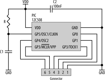
Figure 14-1 shows the schematic for a small computer based on the PIC12C508. The digital I/O signals of the PIC are brought out through a 7-pin connector. If the design were implemented using surface-mount components wherever possible, the connector would be the largest component on the PCB!
This particular PIC processor includes an internal RC oscillator that runs at 4 MHz, so we can use it without any external oscillator circuit. The design in Figure 14-2 shows the same PIC-based design, but this time using an external 32 kHz watch crystal for its oscillator. By running off a (slower) 32 kHz crystal, we have the advantage of greatly reducing the processor’s power consumption. This is important for battery-powered applications.
Two 15 pF capacitors remove unwanted higher-order harmonics from the crystal’s oscillation. The values for the capacitors vary depending on what speed and type of crystal you are using. The processor datasheet has tables showing recommended capacitor values for various crystal frequencies.


Tip
The PIC processor has to be configured to use the appropriate oscillator source. When using the PIC with a 32 kHz crystal, the chip has to be configured in “LP mode.” If you’re using the PIC with faster crystals (greater than 455 kHz), the chip has to be in “XT mode.” The internal RC oscillator is selected by “INTRC mode,” while an external oscillator requires “EXTRC mode.” The Microchip development software (MPLAB) allows you to easily set these parameters when burning software into the processor.
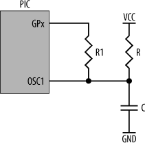
The alternative is to use an external RC circuit as the clock source (Figure 14-3). While not the most precise timing option, it is by far the cheapest. The actual frequency of oscillation depends on a combination of the values of the resistor, the capacitor, the supply voltage, the variation in tolerances for the components, and the current operating temperature. To be clear, only an approximate operating frequency can be determined for an RC oscillator. For stable operation, Microchip recommends that the resistor should be between 3 kΩ and 100 kΩ, and the capacitor greater than 20 pF. If you wish to use an external RC oscillator, refer to the processor’s datasheet, as Microchip has detailed information on RC component selection, taking into account voltage and temperature effects.
Variable-Speed Oscillator
One of the neat tricks you can do if using an external RC oscillator is have a variable-speed computer. This is accomplished by adding a pull-up resistor (R1) between the oscillator input and an I/O pin (Figure 14-4). For normal operation, the I/O pin is configured as an input. By configuring the I/O pin as an output and placing it high, the resistor R1 is effectively placed in parallel with the resistor R. The overall resistance is increased by the relationship RTOTAL = 1 / (1/R + 1/R1), and the oscillator slows accordingly. This is a useful technique to reduce power consumption under software control.
When using an external RC circuit to drive the internal oscillator, an extra PIC I/O line (GP4) becomes available for use.
Power-on Reset
No external reset is needed for this PIC. Instead, the design relies on the internal power-up reset circuit of the processor. Further, not even an external resistor is required on the reset input, ![]() , since the processor incorporates a weak pull-up resistor for this purpose. When not used as a reset input,
, since the processor incorporates a weak pull-up resistor for this purpose. When not used as a reset input, ![]() can be utilized as a general-purpose input.
can be utilized as a general-purpose input.
Warning
![]() on other PIC processors does require either a pull-up resistor or direct connection to V
DD. Leaving it unconnected will not work, nor can it be used as a general-purpose input. Always check the datasheet!
on other PIC processors does require either a pull-up resistor or direct connection to V
DD. Leaving it unconnected will not work, nor can it be used as a general-purpose input. Always check the datasheet!
The power supply (VDD) for the PIC12C805 can range from 2.5 V to 5.5 V.
That covers the basics of a PIC12C805 system, and it’s not that much different from the corresponding AVR computer, which we’ll look at in the next chapter. The real differences lie in their internal architectures (and instruction sets) and in the subtleties of their operating voltages and interfacing capabilities. As you can see, there’s not a lot of hard work involved in putting one of these little machines into your embedded system.
A Bigger PIC
In this section, we’ll look at the PIC16C73 processor. For a mid-range PIC, the design is not dissimilar to the simpler PIC we’ve already seen. The only real difference is that the processor has more pins, more I/O, and more functionality. Designing for PIC17 and PIC18 processors is not dissimilar to creating machines based on the PIC16 family. What you learn here is applicable to many other PICs.
The schematic for this processor is shown in Figure 14-5. This processor has 4K words of program memory, 192 bytes of RAM, and a variety of I/O subsystems, such as three timer modules, SPI, I2C, a UART, five channels of analog input, and up to 22 digital I/O pins.

This processor has one power pin (VDD) and two ground pins (VSS). As always, power is decoupled to ground with a small capacitor (C3). The only other requirements are some form of clock generation—in this case provided by a crystal, X1--and two decoupling capacitors, C1 and C2. The clock could just as easily have been provided using an RC circuit, as we saw with the 12C508 PIC. The reset input, ![]() , is tied directly to the power supply, such that it is permanently inactive. In this case, we are relying on the processor’s internal power-on reset circuitry and don’t need to provide an external reset. It is common practice to use a pull-up resistor to tie an unused input, such as
, is tied directly to the power supply, such that it is permanently inactive. In this case, we are relying on the processor’s internal power-on reset circuitry and don’t need to provide an external reset. It is common practice to use a pull-up resistor to tie an unused input, such as ![]() , inactive. However, in this case I have found that a pull-up resistor can affect the activation of the internal power-on reset to the point where it fails to kick in. (The internal capacitance of the pin combines with the resistor to form an RC circuit, which delays
, inactive. However, in this case I have found that a pull-up resistor can affect the activation of the internal power-on reset to the point where it fails to kick in. (The internal capacitance of the pin combines with the resistor to form an RC circuit, which delays ![]() from reaching the appropriate level.) Thus, the resistor can actually cause the processor to never start properly. So in this case, it’s better to leave it out.
from reaching the appropriate level.) Thus, the resistor can actually cause the processor to never start properly. So in this case, it’s better to leave it out.
Port A (RA0 . . . RA5) functions as an analog input port or a general-purpose digital port. Port B (RB0 . . . RB7) is a general-purpose digital port with weak internal pull-up resistors. Port C (RC0 . . . RC7) can act as a digital port or provide timers, PWM, a serial port, a SPI port, or an I2C interface. Depending on your application, you may use some or all of these pins in your design, connecting to other subsystems as appropriate.
This basic design, in combination with the appropriate datasheet, can be adapted to most other PIC processors that you will come across.
PIC-Based Environmental Datalogger
Now let’s look at a complete system based on a PIC processor. The design presented here is a simplified version of my DL4 datalogger product. This datalogger is designed for extended recording of data (for at least a year), using a minimum of power. It has 1M of nonvolatile memory, capable of retaining data without power for as much as 20 years. The sensors fitted are light and temperature, but you could easily adapt this design to record any analog sensor you like, from acceleration to magnetic field. It’s also small. The entire datalogger fits onto a circuit board smaller than your smallest finger.
The processor is a PIC16LF873A, a variant of the PIC16C73. The “L” means that it is low-power, and the “F” means that it is a flash-based part (rather than EPROM or OTP) that can be reprogrammed in-circuit, making debugging (and life) so much easier. The “8” indicates that the processor includes EEPROM for nonvolatile parameter storage, useful for holding user preferences and machine state. Finally, the “A” tells us that it is a second revision (version) of the silicon. The basic circuit for the processor and its support components is shown in Figure 14-6.

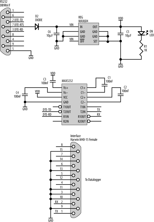
Note that the processor’s power pin is connected to a net labeled PVDD rather than the system’s VDD. Since the processor can be reprogrammed in-circuit, we must consider this in our design. During programming, the burner provides its own supply voltage (+5 V) for the processor. Now the flash chip used in the datalogger requires a nominal supply voltage of 3.3 V, and the 5 V supplied by the burner could potentially damage the chip. Hence, we use a Schottky diode, D2, to isolate the system supply voltage from the processor when it is being reprogrammed. When not being programmed, D2 conducts and supplies the processor with power. During programming, D2 doesn’t conduct, and the rest of the datalogger remains unpowered.
In the same way, we use a Schottky diode (D1) to isolate the processor’s reset pin from the supply voltage. When not being programmed, D1 conducts and pulls ![]() to VDD. However, during programming, D1 isolates
to VDD. However, during programming, D1 isolates ![]() and allows the burner to pull this reset input to a higher voltage as required.
and allows the burner to pull this reset input to a higher voltage as required.
The processor has two crystals, X1 and X2. X1 provides the timing for the processor that drives its internal operation. Depending on our application, X1 could be anything from 32 kHz to 20 MHz. The choice of crystal for X1 affects the power consumption of the datalogger. The faster the crystal, the more juice the machine uses. For ultra-low-power operation, a 32 kHz crystal is the best choice. However, this does have a drawback. Since the internal oscillator is used to drive the UART’s transmitter and receiver clocks, a slow crystal limits the baud rate that we can achieve. Using a 32 kHz crystal gives a maximum baud rate of only 300 baud. Downloading a megabyte of data from the datalogger at that speed takes a whopping 7 hours and 42 minutes! (And you thought your Internet connection was slow.) Hence, you need to choose a value of X1 that best suits your needs. If you can live with a 7-hour download and want the maximum possible operating life from your battery, use a 32 kHz crystal. If battery life is not critical, use a faster crystal.
X2 is used to drive the processor’s internal TIMER1 subsystem, which we use for timekeeping functions and for scheduling the sampling process. While it is possible to use the processor’s main oscillator to drive the internal timers, this oscillator is shut down during the execution of the SLEEP instruction. (The internal watchdog circuit is used to reawaken the processor.) Hence, it is better to use a second crystal on TIMER1 for your timekeeping, as TIMER1 continues to operate even during sleep.
The voltage regulator circuit is shown in Figure 14-7. It’s a standard MAX604 circuit, providing a 3.3 V supply voltage on VDD. Since we are using a battery to supply power, we can live without a capacitor on the input. There’s a huge choice of batteries available. I like the Energizer EL123 battery. It’s relatively small (two-thirds the length of a AA and slightly fatter) and can run the datalogger for well over a year.
The regulator is important in the datalogger for two reasons. First, it ensures that the supply voltage within the datalogger is constant. This is critical, as the supply voltage
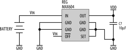
is used as a reference for the analog-to-digital converter. While it is perfectly possible to run the processor directly off a battery, as the battery’s voltage begins to drop with use, the readings from the sensors will become increasingly meaningless. We’d be recording data quite successfully, but its relevance would be nil.
The second reason for using the regulator is that it is able to operate off a lower voltage than other components in the system and still provide a stable 3.3 V. This means that even as our battery is draining, we can still get the maximum operating life possible.
Figure 14-8 shows the nonvolatile flash (made by ST Electronics), which is used for holding data. The flash uses a simple SPI interface to connect to the host processor. It is selected by the FLASH chip select, which is controlled from a processor I/O line (RB2). The HOLD input to flash acts as a “pause” function during accesses. This allows the processor, until software control, to temporarily suspend its access to the flash and perform SPI transfers with other peripherals. This feature currently isn’t used in the datalogger but is included to allow for future functionality, such as the inclusion of digital, SPI-based sensors. Finally, the chip select (FLASH) is pulled high to ensure that the flash is not inadvertently selected as the datalogger is powering up.

Figure 14-9 shows the datalogger’s interface to the outside world. The DL4 datalogger uses a small Harwin connector, also shown in Figure 14-9, but you could use whatever suits your application, even an IDC header.
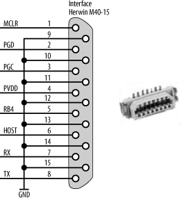
The connector is used to mate with two separate devices. The first is shown in Figure 14-10. This in-house adaptor allows the datalogger to be plugged into a Microchip PICSTART Plus programmer for burning new code. It simply maps the signals required during programming (![]() , PGD, PGC, power, and ground) to the equivalent pins for a DIP-based PIC. In essence, it converts the datalogger’s connector into the pinout of a DIP-based PIC. The adaptor board has pins underneath that insert into the programmer.
, PGD, PGC, power, and ground) to the equivalent pins for a DIP-based PIC. In essence, it converts the datalogger’s connector into the pinout of a DIP-based PIC. The adaptor board has pins underneath that insert into the programmer.

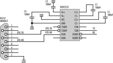
The second device into which the datalogger plugs is an RS-232C adaptor module, shown in Figure 14-11.

This module allows the datalogger to connect to a host computer for both configuration setup and data recovery. The adaptor has a Maxim RS-232C level-shifter and a voltage regulator (both fitted to the top side of the circuit board), and a DB-9 connector. It draws its power from the RTS signal of the host computer’s serial port and, as such, requires no external power supply. The schematic for this circuit is shown in Figure 14-12. Note that this is an independent circuit from that of the datalogger.
The diode D2 is needed since RTS can have negative voltages as well as positive voltages. D2 prevents damage to the regulator when RTS is negative. During normal operation, RTS is set at +12 V by the host computer under software control, turning on the serial adaptor. The regulator turns this +12 V into +3.3 V, which powers the MAX3232 and illuminates the LED. Note that pin 6 of the Harwin connector on the datalogger is connected to a net called HOST. This pin corresponds to pin 3 of the adaptor’s Harwin connector and is tied to ground. When the datalogger is plugged into the adaptor module, HOST is pulled low, but at all other times it is high due to the internal pull-up resistors inside the PIC. In this simple way, software running on the datalogger can tell whether a host computer is present. This is useful as the datalogger’s UART may be disabled to save power until it is required. Further, it can act as a simple switch for the firmware, toggling between “talk to host” mode and “datalogging” mode. It’s interesting to note that the Harwin connector is much bigger on the schematic than the DB-9 due to the number of pins. Yet, when placed next to a DB-9, the Harwin connector is physically tiny.
Finally, Figure 14-13 shows the sensors of the datalogger. These particular sensors are covered in detail in Chapter 13. You could just as easily use other sensors or provide a connector allowing for interfacing to interchangeable sensor modules or external analog subsystems.

Motor Control with a PIC
Now let’s look at using a PIC in a completely different sort of application: motor control via user input. While the design presented in this section is targeted at a specific application, it is just as easily adapted to any task where small DC motors need to be controlled, from tools to robotics.
My young nephews are into model trains, and the standard controller that came with the railroad was a fairly simple device. The speed of the locomotives is controlled by simply varying the voltage on the track. Turn up the voltage, and the trains go faster; turn down the voltage, and the trains stall on dirty rails. Fine control and realistic operation just wasn’t possible. I decided to solve this problem by throwing a little high-tech at it and designed for them a microprocessor-based controller using a PIC. It’s this design that I will share with you.
Tip
I’ve designed literally many dozens of embedded systems over the years, from tiny controllers to small parallel supercomputers, but I have to say that I’ve never had so much fun debugging as when I was debugging the train controller.
The design uses pulse-width modulation (PWM), discussed in Chapter 13, to control the motors inside the locomotives. As PWM uses pulses of fixed amplitude to drive the motor, the problems of low-voltage stalls disappear. Further, since the PWM is controlled by software, very slow speeds can be achieved, giving very realistic operation. The PIC processor has two PWM generation modules inbuilt. Generating PWM with a PIC is just a matter of writing some simple code.
The hardware design takes the basic concept one step further by adding momentum control and braking. The momentum control allows you to specify the mass of the train under control so that when you open up the throttle, the train gradually builds up speed, and rolls to a halt when the throttle is closed. Braking speeds up the stopping. All this sounds complicated, but the hardware to do it is trivially simple when you use a microcontroller. All the real “work” is done in the software, and you can keep it as simple or as fancy as you want.
Tip
There is a much more sophisticated way of controlling model trains called Digital Command Control (DCC), which treats the trackwork as a LAN and sends command packets to the locomotives. This is a published standard and is quite sophisticated. You can read more about it at http://www.dcc.info. The design presented here is not as complicated as DCC, nor is it compatible with DCC. However, it’s certainly a lot cheaper and easier to implement than DCC.
The processor schematic is shown in Figure 14-14. It’s not that different from the one used in the datalogger.
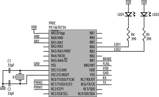
You’ll notice that there’s only one crystal, since there’s no need for timekeeping. Two status LEDs are provided for user feedback by software. As there are several spare pins on Port B (RB2, RB5..7), you could add extra LEDs if you feel so inclined. BRAKE and FLAG are inputs to the processor. BRAKE comes from a push-button switch, and FLAG is an output from the H-bridge chip that indicates an over-current fault.
You’ll also notice that there’s no provision for in-circuit programming as was provided in the datalogger design. For this particular project, I used a DIP-based PIC processor that I had lying around, and to reprogram the part it was a simple matter to remove it from its socket on the circuit board and drop it into the burner. If you want to be able to reprogram the chip in-circuit, simply use the same connections as in the datalogger design.
The choice of crystal frequency is up to you, but the choice you make does have an interesting consequence. The frequency of the crystal relates directly to the PWM frequency the processor is able to generate. The clock signal from the crystal circuit is divided by four before being fed into the processor’s PWM modules. Registers within the PWM modules can then scale this back further to produce a slower PWM frequency. Commercial train controllers use a PWM frequency of 16,125 Hz. Any slower than this and you will hear noise from the motors; any faster and there is a loss of torque. So to achieve a PWM frequency of 16 kHz, you’ll need a crystal with a frequency greater than 64 kHz. As you can’t easily obtain crystals of that exact frequency, the best choice would be a 1 MHz crystal, using the PWM modules’ registers to scale it back appropriately.
Tip
Now, all that is if you don’t want to hear the motors of the locomotives. If your model railroad uses diesels, you may want to choose a crystal frequency of 32 kHz (readily available watch crystal) and scale it back so that the PWM frequency is on the order of tens of Hz. At this frequency, the motors do make a noise, a growling, throbbing sound that sounds very much like a real diesel engine. As the locomotive starts up, the motors produce a sound like a diesel idling, and as it picks up speed, the sound echoes a diesel doing real work.
The voltage regulator circuit is shown in Figure 14-15. The regulator chosen is a standard (and cheap) LM7805 that provides a constant +5 V output from an input voltage of between +7 V and +35 V. Since the motors of model locomotives run on a nominal maximum of +12 V, this is the actual supply voltage for the system. Also included in the regulator schematic is a LED to indicate when power is on and extra decoupling capacitors to help eliminate digital noise in the system.
Figure 14-16 shows the controls used to drive the train. The throttle and momentum controls are simply 50 kΩ potentiometers, which are used as voltage dividers. The wipers of these pots provide a voltage of between 0 V and +5 V to the analog inputs of the PIC. Thus, position of the control can easily be read by software. The direction and brake controls are simple push buttons. The direction control connects directly to an input on the H-bridge chip (discussed shortly), and the brake control is used as a digital input to the processor. The direction control has a 100 kΩ pull-up resistor, and the brake control relies on the internal pull-ups of Port B of the processor.

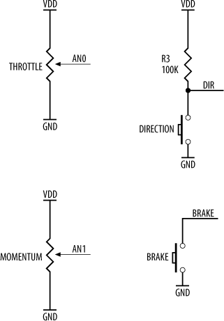
Figure 14-17 shows the H-bridge chip. This converts the PWM output of the processor to voltage levels appropriate for driving the small DC motors found in model locomotives or, for that matter, any sort of small DC motor.

The H-bridge uses VIN (+12 V) as its power source because it must supply that voltage to the motors. As mentioned, the DIR (direction) input comes from a simple push button and determines the polarity of the output. Alternatively, the direction switch could be connected to a spare digital input of the processor, and a digital output could drive DIR. Since it would be a simple mapping of input to output by the software, it’s easier just to connect it straight through and bypass the PIC.
The output of the PIC’s PWM1 module is connected directly to the PWM input of the H-bridge. The H-bridge converts the 5 V amplitude, PWM signal from the PIC to a 12 V amplitude, PWM output whose polarity is determined by DIR.
Tip
You may have noticed that the PIC has two PWM modules. If you wish to control a second motor (train or whatever) with the second module, simply replicate the H-bridge circuit and connect it to PWM2. (Don’t forget to keep the appropriate nets separate by using different net names in your schematic editor.)
The H-bridge has internal over-current sensing and will shut itself off if its temperature rises too high (as would happen if the outputs were shorted together). The FAULT output indicates when this occurs. This active-low output is used to control a LED and is also connected to an input on the processor so that the software can be made aware of the fault condition.
Finally, we can add an optional serial port to the controller, shown in Figure 14-18. This is a standard RS-232C level-shifter circuit and is connected to the RX and TX pins of the processor’s UART. The serial port can be used for software debugging to display status messages to a host computer or terminal. If you wanted to get very fancy, you could use the serial port to allow a host computer to send commands to the train controller. If you’re adapting this design for robotics, a serial port would be a very useful addition. However, if you are providing control from an external host, don’t forget to connect the DIR input of the H-bridge to the PIC and not directly to a push button.
In the next chapter, we’ll take a look at the AVR processor family. These processors are comparable to PICs in terms of I/O and functionality but have a higher throughput and a more versatile architecture.