Chapter 1. An Introduction to Computer Architecture
Each machine has its own, unique personality which probably could be defined as the intuitive sum total of everything you know and feel about it. This personality constantly changes, usually for the worse, but sometimes surprisingly for the better...
—Robert M. Pirsig, Zen and the Art of Motorcycle Maintenance
This book is about designing and building specialized computers. We all know what a computer is. It’s that box that sits on your desk, quietly purring away (or rattling if the fan is shot), running your programs and regularly crashing (if you’re not running some variety of Unix). Inside that box is the electronics that runs your software, stores your information, and connects you to the world. It’s all about processing information. Designing a computer, therefore, is about designing a machine that holds and manipulates data.
Computer systems fall into essentially two separate categories. The first, and most obvious, is that of the desktop computer. When you say “computer” to someone, this is the machine that usually comes to her mind. The second type of computer is the embedded computer, a computer that is integrated into another system for the purposes of control and/or monitoring. Embedded computers are far more numerous than desktop systems, but far less obvious. Ask the average person how many computers he has in his home, and he might reply that he has one or two. In fact, he may have 30 or more, hidden inside his TVs, VCRs, DVD players, remote controls, washing machines, cell phones, air conditioners, game consoles, ovens, toys, and a host of other devices.
In this chapter, we’ll look at computer architecture in general. This is applicable to both embedded and desktop computers, because the primary difference between an embedded machine and a general-purpose computer is its application. The basic principles of operation and the underlying architectures are fundamentally the same.
Both have a processor, memory, and often several forms of input and output. The primary difference lies in their intended use, and this is reflected in the system design and their software. Desktop computers can run a variety of application programs, with system resources orchestrated by an operating system. By running different application programs, the functionality of the desktop computer is changed. One moment, it may be used as a word processor; the next it is an MP3 player or a database client. Which software is loaded and run is under user control.
In contrast, the embedded computer is normally dedicated to a specific task. In many cases, an embedded system is used to replace application-specific electronics. The advantage of using an embedded microprocessor over dedicated electronics is that the functionality of the system is determined by the software, not the hardware. This makes the embedded system easier to produce, and much easier to evolve, than a complicated circuit.
The embedded system typically has one application and one application only, which is permanently running. The embedded computer may or may not have an operating system, and rarely does it provide the user with the ability to arbitrarily install new software. The software is normally contained in the system’s nonvolatile memory, unlike a desktop computer where the nonvolatile memory contains boot software and (maybe) low-level drivers only.
Embedded hardware is often much simpler than a desktop system, but it can also be far more complex too. An embedded computer may be implemented in a single chip with just a few support components, and its purpose may be as crude as a controller for a garden-watering system. Alternatively, the embedded computer may be a 150-processor, distributed parallel machine responsible for all the flight and control systems of a commercial jet. As diverse as embedded hardware may be, the underlying principles of design are the same.
This chapter introduces some important concepts relating to computer architecture, with specific emphasis on those topics relevant to embedded systems. Its purpose is to give you grounding before moving on to the more hands-on information that begins in Chapter 2. In this chapter, you’ll learn about the basics of processors, interrupts, the difference between RISC and CISC, parallel systems, memory, and I/O.
Concepts
In essence, a computer is a machine designed to process, store, and retrieve data. Data may be numbers in a spreadsheet, characters of text in a document, dots of color in an image, waveforms of sound, or the state of some system, such as an air conditioner or a CD player. All data is stored in the computer as numbers. It’s easy to forget this when we’re deep in C code, contemplating complex algorithms and data structures.
The computer manipulates the data by performing operations on the numbers. Displaying an image on a screen is accomplished by moving an array of numbers to the video memory, each number representing a pixel of color. To play an MP3 audio file, the computer reads an array of numbers from disk and into memory, manipulates those numbers to convert the compressed audio data into raw audio data, and then outputs the new set of numbers (the raw audio data) to the audio chip.
Everything that a computer does, from web browsing to printing, involves moving and processing numbers. The electronics of a computer is nothing more than a system designed to hold, move, and change numbers.
A computer system is composed of many parts, both hardware and software. At the heart of the computer is the processor, the hardware that executes the computer programs. The computer also has memory, often several different types in one system. The memory is used to store programs while the processor is running them, as well as store the data that the programs are manipulating. The computer also has devices for storing data, or exchanging data with the outside world. These may allow the input of text via a keyboard, the display of information on a screen, or the movement of programs and data to or from a disk drive.
The software controls the operation and functionality of the computer. There are many “layers” of software in the computer (Figure 1-1). Typically, a given layer will only interact with the layers immediately above or below it.

At the lowest level, there are programs that are run by the processor when the computer first powers up. These programs initialize the other hardware subsystems to a known state and configure the computer for correct operation. This software, because it is permanently stored in the computer’s memory, is known as firmware .
The bootloader is located in the firmware. The bootloader is a special program run by the processor that reads the operating system from disk (or nonvolatile memory or network interface) and places it in memory so that the processor may then run it. The bootloader is present in desktop computers and workstations, and may be present in some embedded computers.
Above the firmware, the operating system controls the operation of the computer. It organizes the use of memory and controls devices such as the keyboard, mouse, screen, disk drives, and so on. It is also the software that often provides an interface to the user, enabling her to run application programs and access her files on disk. The operating system typically provides a set of software tools for application programs, providing a mechanism by which they too can access the screen, disk drives, and so on. Not all embedded systems use or even need an operating system. Often, an embedded system will simply run code dedicated to its task, and the presence of an operating system is overkill. In other instances, such as network routers, an operating system provides necessary software integration and greatly simplifies the development process. Whether an operating system is needed and useful really depends on the intended purpose of the embedded computer and, to a lesser degree, on the preference of the designer.
At the highest level, the application software constitutes the programs that provide the functionality of the computer. Everything below the application is considered system software . For embedded computers, the boundary between application and system software is often blurred. This reflects the underlying principle in embedded design that a system should be designed to achieve its objective in as simple and straightforward a manner as possible.
Processors
The processor is the most important part of a computer, the component around which everything else is centered. In essence, the processor is the computing part of the computer. A processor is an electronic device capable of manipulating data (information) in a way specified by a sequence of instructions. The instructions are also known as opcodes or machine code . This sequence of instructions may be altered to suit the application, and, hence, computers are programmable. A sequence of instructions is what constitutes a program.
Instructions in a computer are numbers, just like data. Different numbers, when read and executed by a processor, cause different things to happen. A good analogy is the mechanism of a music box. A music box has a rotating drum with little bumps, and a row of prongs. As the drum rotates, different prongs in turn are activated by the bumps, and music is produced. In a similar way, the bit patterns of instructions feed into the execution unit of the processor. Different bit patterns activate or deactivate different parts of the processing core. Thus, the bit pattern of a given instruction may activate an addition operation, while another bit pattern may cause a byte to be stored to memory.
A sequence of instructions is a machine-code program. Each type of processor has a different instruction set, meaning that the functionality of the instructions (and the bit patterns that activate them) varies. Processor instructions are often quite simple, such as “add two numbers” or “call this function.” In some processors, however, they can be as complex and sophisticated as “if the result of the last operation was zero, then use this particular number to reference another number in memory, and then increment the first number once you’ve finished.” This will be covered in more detail in the section on CISC and RISC processors, later in this chapter.
Basic System Architecture
The processor alone is incapable of successfully performing any tasks. It requires memory (for program and data storage), support logic, and at least one I/O device (“input/output device”) used to transfer data between the computer and the outside world. The basic computer system is shown in Figure 1-2.

A microprocessor is a processor implemented (usually) on a single, integrated circuit. With the exception of those found in some large supercomputers, nearly all modern processors are microprocessors, and the two terms are often used interchangeably. Common microprocessors in use today are the Intel Pentium series, Freescale/IBM PowerPC, MIPS, ARM, and the Sun SPARC, among others. A microprocessor is sometimes also known as a CPU (Central Processing Unit).
A microcontroller is a processor, memory, and some I/O devices contained within a single, integrated circuit, and intended for use in embedded systems. The buses that interconnect the processor with its I/O exist within the same integrated circuit. The range of available microcontrollers is very broad. They range from the tiny PICs and AVRs (to be covered in this book) to PowerPC processors with built-in I/O, intended for embedded applications. In this book, we will look at both microprocessors and microcontrollers.
Microcontrollers are very similar to System-on-Chip (SoC) processors, intended for use in conventional computers such as PCs and workstations. SoC processors have a different suite of I/O, reflecting their intended application, and are designed to be interfaced to large banks of external memory. Microcontrollers usually have all their memory on-chip and may provide only limited support for external memory devices.
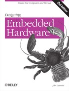
The memory of the computer system contains both the instructions that the processor will execute and the data it will manipulate. The memory of a computer system is never empty. It always contains something, whether it be instructions, meaningful data, or just the random garbage that appeared in the memory when the system powered up.
Instructions are read (fetched) from memory, while data is both read from and written to memory, as shown in Figure 1-3.
This form of computer architecture is known as a Von Neumann machine, named after John Von Neumann, one of the originators of the concept. With very few exceptions, nearly all modern computers follow this form. Von Neumann computers are what can be termed control-flow computers. The steps taken by the computer are governed by the sequential control of a program. In other words, the computer follows a step-by-step program that governs its operation.
Tip
There are some interesting non-Von Neumann architectures, such as the massively parallel Connection Machine and the nascent efforts at building biological and quantum computers, or neural networks.
A classical Von Neumann machine has several distinguishing characteristics:
- There is no real difference between data and instructions .
A processor can be directed to begin execution at a given point in memory, and it has no way of knowing whether the sequence of numbers beginning at that point is data or instructions. The instruction 0x4143 may also be data (the number 0x4143, or the ASCII characters “A” and “C”). The processor has no way of telling what is data or what is an instruction. If a number is to be executed by the processor, it is an instruction; if it is to be manipulated, it is data.
Because of this lack of distinction, the processor is capable of changing its instructions (treating them as data) under program control. And because the processor has no way of distinguishing between data and instruction, it will blindly execute anything that it is given, whether it is a meaningful sequence of instructions or not.
- Data has no inherent meaning .
There is nothing to distinguish between a number that represents a dot of color in an image and a number that represents a character in a text document. Meaning comes from how these numbers are treated under the execution of a program.
- Data and instructions share the same memory .
This means that sequences of instructions in a program may be treated as data by another program. A compiler creates a program binary by generating a sequence of numbers (instructions) in memory. To the compiler, the compiled program is just data, and it is treated as such. It is a program only when the processor begins execution. Similarly, an operating system loading an application program from disk does so by treating the sequence of instructions of that program as data. The program is loaded to memory just as an image or text file would be, and this is possible due to the shared memory space.
- Memory is a linear (one-dimensional) array of storage locations .
The processor’s memory space may contain the operating system, various programs, and their associated data, all within the same linear space.
Each location in the memory space has a unique, sequential address. The address of a memory location is used to specify (and select) that location. The memory space is also known as the address space , and how that address space is partitioned between different memory and I/O devices is known as the memory map . The address space is the array of all addressable memory locations. In an 8-bit processor (such as the 68HC11) with a 16-bit address bus, this works out to be 216 = 65,536 = 64K of memory. Hence, the processor is said to have a 64K address space. Processors with 32-bit address buses can access 232 = 4,294,967,296 = 4G of memory.
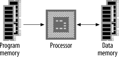
Some processors, notably the Intel x86 family, have a separate address space for I/O devices with separate instructions for accessing this space. This is known as ported I/O . However, most processors make no distinction between memory devices and I/O devices within the address space. I/O devices exist within the same linear space as memory devices, and the same instructions are used to access each. This is known as memory-mapped I/O (Figure 1-4). Memory-mapped I/O is certainly the most common form. Ported I/O address spaces are becoming rare, and the use of the term even rarer.
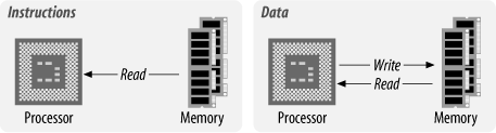
Most microprocessors available are standard Von Neumann machines. The main deviation from this is the Harvard architecture , in which instructions and data have different memory spaces (Figure 1-5) with separate address, data, and control buses for each memory space. This has a number of advantages in that instruction and data fetches can occur concurrently, and the size of an instruction is not set by the size of the standard data unit (word).

Buses
A bus is a physical group of signal lines that have a related function. Buses allow for the transfer of electrical signals between different parts of the computer system and thereby transfer information from one device to another. For example, the data bus is the group of signal lines that carry data between the processor and the various subsystems that comprise the computer. The “width” of a bus is the number of signal lines dedicated to transferring information. For example, an 8-bit-wide bus transfers 8 bits of data in parallel.
The majority of microprocessors available today (with some exceptions) use the three-bus system architecture (Figure 1-6). The three buses are the address bus , the data bus, and the control bus .
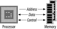
The data bus is bidirectional, the direction of transfer being determined by the processor. The address bus carries the address, which points to the location in memory that the processor is attempting to access. It is the job of external circuitry to determine in which external device a given memory location exists and to activate that device. This is known as address decoding . The control bus carries information from the processor about the state of the current access, such as whether it is a write or a read operation. The control bus can also carry information back to the processor regarding the current access, such as an address error. Different processors have different control lines, but there are some control lines that are common among many processors. The control bus may consist of output signals such as read, write, valid address, etc. A processor usually has several input control lines too, such as reset, one or more interrupt lines, and a clock input.
Tip
A few years ago, I had the opportunity to wander through, in, and around CSIRAC (pronounced “sigh-rack”). This was one of the world’s first digital computers, designed and built in Sydney, Australia, in the late 1940s. It was a massive machine, filling a very big room with the type of solid hardware that you can really kick. It was quite an experience looking over the old machine. I remember at one stage walking through the disk controller (it was the size of small room) and looking up at a mass of wires strung overhead. I asked what they were for. “That’s the data bus!” came the reply.
CSIRAC is now housed in the museum of the University of Melbourne. You can take an online tour of the machine, and even download a simulator, at http://www.cs.mu.oz.au/csirac.
Processor operation
There are six basic types of access that a processor can perform with external chips. The processor can write data to memory or write data to an I/O device, read data from memory or read data from an I/O device, read instructions from memory, and perform internal manipulation of data within the processor.
In many systems, writing data to memory is functionally identical to writing data to an I/O device. Similarly, reading data from memory constitutes the same external operation as reading data from an I/O device, or reading an instruction from memory. In other words, the processor makes no distinction between memory and I/O.
The internal data storage of the processor is known as its registers . The processor has a limited number of registers, and these are used to hold the current data/operands that the processor is manipulating.
ALU
The Arithmetic Logic Unit (ALU) performs the internal arithmetic manipulation of data in the processor. The instructions that are read and executed by the processor control the data flow between the registers and the ALU. The instructions also control the arithmetic operations performed by the ALU via the ALU’s control inputs. A symbolic representation of an ALU is shown in Figure 1-7.

Whenever instructed by the processor, the ALU performs an operation (typically one of addition, subtraction, NOT, AND, OR, XOR, shift left/right, or rotate left/right) on one or more values. These values, called operands , are typically obtained from two registers, or from one register and a memory location. The result of the operation is then placed back into a given destination register or memory location. The status outputs indicate any special attributes about the operation, such as whether the result was zero, negative, or if an overflow or carry occurred. Some processors have separate units for multiplication and division, and for bit shifting, providing faster operation and increased throughput.
Each architecture has its own unique ALU features, and this can vary greatly from one processor to another. However, all are just variations on a theme, and all share the common characteristics just described.
Interrupts
Interrupts (also known as traps or exceptions in some processors) are a technique of diverting the processor from the execution of the current program so that it may deal with some event that has occurred. Such an event may be an error from a peripheral, or simply that an I/O device has finished the last task it was given and is now ready for another. An interrupt is generated in your computer every time you type a key or move the mouse. You can think of it as a hardware-generated function call.
Interrupts free the processor from having to continuously check the I/O devices to determine whether they require service. Instead, the processor may continue with other tasks. The I/O devices will notify it when they require attention by asserting one of the processor’s interrupt inputs. Interrupts can be of varying priorities in some processors, thereby assigning differing importance to the events that can interrupt the processor. If the processor is servicing a low-priority interrupt, it will pause it in order to service a higher-priority interrupt. However, if the processor is servicing an interrupt and a second, lower-priority interrupt occurs, the processor will ignore that interrupt until it has finished the higher-priority service.
When an interrupt occurs, the usual procedure is for the processor to save its state by pushing its registers and program counter onto the stack. The processor then loads an interrupt vector into the program counter. The interrupt vector is the address at which an interrupt service routine (ISR) lies. Thus, loading the vector into the program counter causes the processor to begin execution of the ISR, performing whatever service the interrupting device required. The last instruction of an ISR is always a Return from Interrupt instruction. This causes the processor to reload its saved state (registers and program counter) from the stack and resume its original program. Interrupts are largely transparent to the original program. This means that the original program is completely “unaware” that the processor was interrupted, save for a lost interval of time.
Processors with shadow registers use these to save their current state, rather than pushing their register bank onto the stack. This saves considerable memory accesses (and therefore time) when processing an interrupt. However, since only one set of shadow registers exists, a processor servicing multiple interrupts must “manually” preserve the state of the registers before servicing the higher interrupt. If it does not, important state information will be lost. Upon returning from an ISR, the contents of the shadow registers are swapped back into the main register array.
Hardware interrupts
There are two ways of telling when an I/O device (such as a serial controller or a disk controller) is ready for the next sequence of data to be transferred. The first is busy waiting or polling , where the processor continuously checks the device’s status register until the device is ready. This wastes the processor’s time but is the simplest to implement. For some time-critical applications, polling can reduce the time it takes for the processor to respond to a change of state in a peripheral.
A better way is for the device to generate an interrupt to the processor when it is ready for a transfer to take place. Small, simple processors may only have one (or two) interrupt inputs, so several external devices may have to share the interrupt lines of the processor. When an interrupt occurs, the processor must check each device to determine which one generated the interrupt. (This can also be considered a form of polling.) The advantage of interrupt polling over ordinary polling is that the polling occurs only when there is a need to service a device. Polling interrupts is suitable only in systems that have a small number of devices; otherwise, the processor will spend too long trying to determine the source of the interrupt.
The other technique of servicing an interrupt is by using vectored interrupts,[*] by which the interrupting device provides the interrupt vector that the processor is to take. Vectored interrupts reduce considerably the time it takes the processor to determine the source of the interrupt. If an interrupt request can be generated from more than one source, it is therefore necessary to assign priorities (levels) to the different interrupts. This can be done in either hardware or software, depending on the particular application. In this scheme, the processor has numerous interrupt lines, with each interrupt corresponding to a given interrupt vector. So, for example, when an interrupt of priority 7 occurs (interrupt lines corresponding to “7” are asserted), the processor loads vector 7 into its program counter and starts executing the service routine specific to interrupt 7.
Vectored interrupts can be taken one step further. Some processors and devices support the device by actually placing the appropriate vector onto the data bus when they generate an interrupt. This means the system can be even more versatile, so that instead of being limited to one interrupt per peripheral, each device can supply an interrupt vector specific to the event that is causing the interrupt. However, the processor must support this function, and most do not.
Some processors have a feature known as a fast hardware interrupt. With this interrupt, only the program counter is saved. It assumes that the ISR will protect the contents of the registers by manually saving their state as required. Fast interrupts are useful when an I/O device requires a very fast response from a processor and cannot wait for the processor to save all its registers to the stack. A special (and separate) interrupt line is used to generate fast interrupts.
Software interrupts
A software interrupt is generated by an instruction. It is the lowest-priority interrupt and is generally used by programs to request a service to be performed by the system software (operating system or firmware).
So why are software interrupts used? Why isn’t the appropriate section of code called directly? For that matter, why use an operating system to perform tasks for us at all? It gets back to compatibility. Jumping to a subroutine (calling a function) is jumping to a specific address in memory. A future version of the system software may not locate the subroutines at the same addresses as earlier versions. By using a software interrupt, our program does not need to know where the routines lie. It relies on the entry in the vector table to direct it to the correct location.
CISC and RISC
There are two major approaches to processor architecture: Complex Instruction Set Computer (CISC, pronounced “Sisk”) processors and Reduced Instruction Set Computer (RISC) processors. Classic CISC processors are the Intel x86, Motorola 68xxx, and National Semiconductor 32xxx processors, and, to a lesser degree, the Intel Pentium. Common RISC architectures are the Freescale/IBM PowerPC, the MIPS architecture, Sun’s SPARC, the ARM, the Atmel AVR, and the Microchip PIC.
CISC processors have a single processing unit, external memory, and a relatively small register set and many hundreds of different instructions. In many ways, they are just smaller versions of the processing units of mainframe computers from the 1960s.
The tendency in processor design throughout the late 70s and early 80s was toward bigger and more complicated instruction sets. Need to input a string of characters from an I/O port? Well, with CISC (80x86 family), there’s a single instruction to do it! The diversity of instructions in a CISC processor can run to well over 1,000 opcodes in some processors, such as the Motorola 68000. This had the advantage of making the job of the assembly-language programmer easier, since you had to write fewer lines of code to get the job done. As memory was slow and expensive, it also made sense to make each instruction do more. This reduced the number of instructions needed to perform a given function, and thereby reduced memory space and the number of memory accesses required to fetch instructions. As memory got cheaper and faster, and compilers became more efficient, the relative advantages of the CISC approach began to diminish. One main disadvantage of CISC is that the processors themselves get increasingly complicated as a consequence of supporting such a large and diverse instruction set. The control and instruction decode units are complex and slow, the silicon is large and hard to produce, and they consume a lot of power and therefore generate a lot of heat. As processors became more advanced, the overheads that CISC imposed on the silicon became oppressive.
A given processor feature when considered alone may increase processor performance but may actually decrease the performance of the total system, if it increases the total complexity of the device. It was found that by streamlining the instruction set to the most commonly used instructions, the processors become simpler and faster. Fewer cycles are required to decode and execute each instruction, and the cycles are shorter. The drawback is that more (simpler) instructions are required to perform a task, but this is more than made up for in the performance boost to the processor. For example, if both cycle time and the number of cycles per instruction are each reduced by a factor of four, while the number of instructions required to perform a task grows by 50%, the execution of the processor is sped up by a factor of eight.
The realization of this led to a rethink of processor design. The result was the RISC architecture, which has led to the development of very high-performance processors. The basic philosophy behind RISC is to move the complexity from the silicon to the language compiler. The hardware is kept as simple and fast as possible.
A given complex instruction can be performed by a sequence of much simpler instructions. For example, many processors have an xor (exclusive OR) instruction for bit manipulation, and they also have a clear instruction to set a given register to zero. However, a register can also be set to zero by xor-ing it with itself. Thus, the separate clear instruction is no longer required. It can be replaced with the already present xor. Further, many processors are able to clear a memory location directly by writing a zero to it. That same function can be implemented by clearing a register and then storing that register to the memory location. The instruction to load a register with a literal number can be replaced with the instruction for clearing a register, followed by an add instruction with the literal number as its operand. Thus, six instructions (xor, clear
reg
, clear
memory
, load
literal
, store, and add) can be replaced with just three (xor, store, and add).
So the following CISC assembly pseudocode:
clear 0x1000    ; clear memory location 0x1000
load  r1,#5     ; load register 1 with the value 5
becomes the following RISC pseudocode:
xor   r1,r1      ; clear register 1
store r1,0x1000  ; clear memory location 0x1000
add   r1,#5      ; load register 1 with the value 5
The resulting code size is bigger, but the reduced complexity of the instruction decode unit can result in faster overall operation. Dozens of such code optimizations exist to give RISC its simplicity.
RISC processors have a number of distinguishing characteristics. They have large register sets (in some architectures numbering over 1,000), thereby reducing the number of times the processor must access main memory. Often-used variables can be left inside the processor, reducing the number of accesses to (slow) external memory. Compilers of high-level languages (such as C) take advantage of this to optimize processor performance.
By having smaller and simpler instruction decode units, RISC processors have fast instruction execution, and this also reduces the size and power consumption of the processing unit. Generally, RISC instructions will take only one or two cycles to execute (this depends greatly on the particular processor). This is in contrast to instructions for a CISC processor, whose instructions may take many tens of cycles to execute. For example, one instruction (integer multiplication) on an 80486 CISC processor takes 42 cycles to complete. The same instruction on a RISC processor may take just one cycle. Instructions on a RISC processor have a simple format. All instructions are generally the same length (which makes instruction decode units simpler).
RISC processors implement what is known as a “load/store” architecture. This means that the only instructions that actually reference memory are load and store. In contrast, many (most) instructions on a CISC processor may access or manipulate memory. On a RISC processor, all other instructions (aside from load and store) work on the registers only. This facilitates the ability of RISC processors to complete (most of) their instructions in a single cycle. Consequently, RISC processors do not have the range of addressing modes that are found on CISC processors.
RISC processors also often have pipelined instruction execution. This means that while one instruction is being executed, the next instruction in the sequence is being decoded, while the third one is being fetched. At any given moment, several instructions will be in the pipeline and in the process of being executed. Again, this provides improved processor performance. Thus, even though not all instructions may be completed in a single cycle, the processor may issue and retire instructions on each cycle, thereby achieving effective single-cycle execution. Some RISC processors have overlapped instruction execution, in which load operations may allow the execution of subsequent, unrelated instructions to continue before the data requested by the load has been returned from memory. This allows these instructions to overlap the load, thereby improving processor performance.
Due to their low power consumption and computing power, RISC processors are becoming widely used, particularly in embedded computer systems, and many RISC attributes are appearing in what are traditionally CISC architectures (such as with the Intel Pentium). Ironically, many RISC architectures are adding some CISC-like features, and so the distinction between RISC and CISC is blurring.
An excellent discussion of RISC architectures and processor performance topics can be found in Kevin Dowd and Charles Severance’s High Performance Computing (O’Reilly).
So, which is better for embedded and industrial applications, RISC or CISC? If power consumption needs to be low, then RISC is probably the better architecture to use. However, if the available space for program storage is small, then a CISC processor may be a better alternative, since CISC instructions get more “bang” for the byte.
Digital Signal Processors
A special type of processor architecture is that of the Digital Signal Processor ( DSP ). These processors have instruction sets and architectures optimized for numerical processing of array data. They often extend the Harvard architecture concept further by not only having separate data and code spaces, but also by splitting the data spaces into two or more banks. This allows concurrent instruction fetch and data accesses for multiple operands. As such, DSPs can have very high throughput and can outperform both CISC and RISC processors in certain applications.
DSPs have special hardware well suited to numerical processing of arrays. They often have hardware looping , whereby special registers allow for and control the repeated execution of an instruction sequence. This is also often known as zero-overhead looping , since no conditions need to be explicitly tested by the software as part of the looping process. DSPs often have dedicated hardware for increasing the speed of arithmetic operations. High-speed multipliers, Multiply-And-Accumulate (MAC) units, and barrel shifters are common features.
DSP processors are commonly used in embedded applications, and many conventional embedded microcontrollers include some DSP functionality.
Memory
Memory is used to hold data and software for the processor. There is a variety of memory types, and often a mix is used within a single system. Some memory will retain its contents while there is no power, yet will be slow to access. Other memory devices will be high-capacity, yet will require additional support circuitry and will be slower to access. Still other memory devices will trade capacity for speed, yielding relatively small devices, yet will be capable of keeping up with the fastest of processors.
Memory chips can be organized in two ways, either in word-organized or bit-organized schemes. In the word-organized scheme, complete nybbles, bytes, or words are stored within a single component, whereas with bit-organized memory, each bit of a byte or word is allocated to a separate component (Figure 1-8).

Memory chips come in different sizes, with the width specified as part of the size description. For instance, a DRAM (dynamic RAM) chip might be described as being 4M×1 (bit-organized), whereas a SRAM (static RAM) may be 512K×8 (word-organized). In both cases, each chip has exactly the same storage capacity, but organized in different ways. In the DRAM case, it would take eight chips to complete a memory block for an 8-bit data bus, whereas the SRAM would only require one chip.However, because the DRAMs are organized in parallel, they are accessed simultaneously. The final size of the DRAM block is (4M×1)×8 devices, which is 32M. It is common practice for multiple DRAMs to be placed on a memory module. This is the common way that DRAMs are installed in standard computers.
The common widths for memory chips are x1, x4, and x8, although x16 devices are available. A 32-bit-wide bus can be implemented with thirty-two x1 devices, eight x4 devices, or four x8 devices.
RAM
RAM stands for Random Access Memory. This is a bit of a misnomer, since most (all) computer memory may be considered “random access.” RAM is the “working memory” in the computer system. It is where the processor may easily write data for temporary storage. RAM is generally volatile, losing its contents when the system loses power. Any information stored in RAM that must be retained must be written to some form of permanent storage before the system powers down. There are special nonvolatile RAMs that integrate a battery-backup system, such that the RAM remains powered even when the rest of the computer system has shut down.
RAMs generally fall into two categories: static RAM (also known as SRAM) and dynamic RAM (also known as DRAM).
SRAMs use pairs of logic gates to hold each bit of data. SRAMs are the fastest form of RAM available, require little external support circuitry, and have relatively low power consumption. Their drawbacks are that their capacity is considerably less than DRAM, while being much more expensive. Their relatively low capacity requires more chips to be used to implement the same amount of memory. A modern PC built using nothing but SRAM would be a considerably bigger machine and would cost a small fortune to produce. (It would be very fast, however.)
DRAM uses arrays of what are essentially capacitors to hold individual bits of data. The capacitor arrays will hold their charge only for a short period before it begins to diminish. Therefore, DRAMs need continuous refreshing, every few milliseconds or so. This perpetual need for refreshing requires additional support and can delay processor access to the memory. If a processor access conflicts with the need to refresh the array, the refresh cycle must take precedence.
DRAMs are the highest-capacity memory devices available and come in a wide and diverse variety of subspecies. Interfacing DRAMs to small microcontrollers is generally not possible, and certainly not practical. Most processors with large address spaces include support for DRAMs. Connecting DRAMs to such processors is simply a case of “connecting the dots” (or pins, as the case may be). For those processors that do not include DRAM support, special DRAM controller chips are available that make interfacing the DRAMs very simple indeed.
Many processors have instruction and/or data caches , which store recent memory accesses. These caches are (often, but not always) internal to the processors and are implemented with fast memory cells and high-speed data paths. Instruction execution normally runs out of the instruction cache, providing for fast execution. The processor is capable of rapidly reloading the caches from main memory should a cache miss occur. Some processors have logic that is able to anticipate a cache miss and begin the cache reload prior to the cache miss occurring. Caches are implemented using very fast SRAM and are most often used in large systems to compensate for the slowness of DRAM.
ROM
ROM stands for Read-Only Memory. This is also a bit of a misnomer, since many (modern) ROMs can also be written to. ROMs are nonvolatile memory, requiring no power to retain their contents. They are generally slower than RAM, and considerably slower than fast static RAM.
The primary purpose of ROM within a system is to hold the code (and sometimes data) that needs to be present at power-up. Such software is generally known as firmware and contains software to initialize the computer by placing I/O devices into a known state. It may contain either a bootloader program to load an operating system off disk or network or, in the case of an embedded system, it may contain the application itself.
Many microcontrollers contain on-chip ROM, thereby reducing component count and simplifying system design.
Standard ROM is fabricated (in a simplistic sense) from a large array of diodes. The unwritten bit state for a ROM is all 1s, each byte location reading as 0xFF. The process of loading software into a ROM is known as burning the ROM. This term comes from the fact that the programming process is performed by passing a sufficiently large current through the appropriate diodes to “blow them,” or burn them, thereby creating a zero at that bit location. A device known as a ROM burner can accomplish this, or, if the system supports it, the ROM may be programmed in-circuit. This is known as In-System Programming (ISP) or, sometimes, In-Circuit Programming (ICP).
One-Time Programmable (OTP) ROMs, as the name implies, can be burned once only. Computer manufacturers typically use them in systems where the firmware is stable and the product is shipping in bulk to customers. Mask-programmable ROMs are also one-time programmable, but unlike OTPs, they are burned by the chip manufacturer prior to shipping. Like OTPs, they are used once the software is known to be stable and have the advantage of lowering production costs for large shipments.
EPROM
OTP ROMs are great for shipping in final products, but they are wasteful for debugging, since with each iteration of code change, a new chip must be burned and the old one thrown away. As such, OTPs make for a very expensive development option. No sane person uses OTPs for development work.
A (slightly) better choice for system development and debugging is the Erasable Programmable Read-Only Memory, or EPROM. Shining ultraviolet light through a small window on the top of the chip can erase the EPROM, allowing it to be reprogrammed and reused. They are pin- and signal-compatible with comparable OTP and mask devices. Thus, an EPROM can be used during development, while OTPs can be used in production with no change to the rest of the system.
EPROMs and their equivalent OTP cousins range in capacity from a few kilobytes (exceedingly rare these days) to a megabyte or more.
The drawback with EPROM technology is that the chip must be removed from the circuit to be erased, and the erasure can take many minutes to complete. The chip is then inserted into the burner, loaded with software, and then placed back in-circuit. This can lead to very slow debug cycles. Further, it makes the device useless for storing changeable system parameters. EPROMs are relatively rare these days. You can still buy them, but flash-based memory (to be discussed shortly) is far more common and is the medium of choice.
EEROM
EEROM is Electrically Erasable Read-Only Memory, also known as EEPROM (Electrically Erasable Programmable Read-Only Memory). Very rarely, it is also called Electrically Alterable Read-Only Memory (EAROM). EEROM can be pronounced as either “e-e ROM” or “e-squared ROM,” or sometimes just “e-squared” for short.
EEROMs can be erased and reprogrammed in-circuit. Their capacity is significantly smaller than standard ROM (typically only a few kilobytes), and so they are not suited to holding firmware. Instead, they are typically used for holding system parameters and mode information to be retained during power-off.
It is common for many microcontrollers to incorporate a small EEROM on-chip for holding system parameters. This is especially useful in embedded systems and may be used for storing network addresses, configuration settings, serial numbers, servicing records, and so on.
Flash
Flash is the newest ROM technology and is now dominant. Flash memory has the reprogrammability of EEROM and the large capacity of standard ROMs. Flash chips are sometimes referred to as “flash ROMs” or “flash RAMs.” Since they are not like standard ROMs or standard RAMs, I prefer just to call them “flash” and save on the confusion.
Flash is normally organized as sectors and has the advantage that individual sectors may be erased and rewritten without affecting the contents of the rest of the device. Typically, before a sector can be written, it must be erased. It can’t just be written over as with a RAM.
There are several different flash technologies, and the erasing and programming requirements of flash devices vary from manufacturer to manufacturer.
Input/Output
The address space of the processor can contain devices other than memory. These are input/output devices (I/O devices, also known as peripherals ) and are used by the processor to communicate with the external world. Some examples are serial controllers that communicate with keyboards, mice, modems, etc.; parallel I/O devices that control some external subsystem; or disk-drive controllers, video and audio controllers, or network interfaces.
There are three main ways in which data may be exchanged with the external world:
- Programmed I/O
The processor accepts or delivers data at times convenient to it (the processor).
- Interrupt-driven I/O
External events control the processor by requesting the current program be suspended and the external event be serviced. An external device will interrupt the processor (assert an interrupt control line into the processor), at which time the processor will suspend the current task (program) and begin executing an interrupt service routine. The service of an interrupt may involve transferring data from input to memory, or from memory to output.
- Direct Memory Access (DMA)
DMA allows data to be transferred from I/O devices to memory directly without the continuous involvement of the processor. DMA is used in high-speed systems, where the rate of data transfer is important. Not all processors support DMA.
DMA
DMA is a way of streamlining transfers of large blocks of data between two sections of memory, or between memory and an I/O device. Let’s say you want to read in 100M from disk and store it in memory. You have two options.
One option is for the processor to read one byte at a time from the disk controller into a register and then store the contents of the register to the appropriate memory location. For each byte transferred, the processor must read an instruction, decode the instruction, read the data, read the next instruction, decode the instruction, and then store the data. Then the process starts over again for the next byte.
The second option in moving large amounts of data around the system is DMA. A special device, called a DMA Controller (DMAC), performs high-speed transfers between memory and I/O devices. Using DMA bypasses the processor by setting up a channel between the I/O device and the memory. Thus, data is read from the I/O device and written into memory without the need to execute code to perform the transfer on a byte-by-byte (or word-by-word) basis.
In order for a DMA transfer to occur, the DMAC must have use of the address and data buses. There are several ways in which this could be implemented by the system designer. The most common approach (and probably the simplest) is to suspend the operation of the processor and for the processor to “release” its buses (the buses are tristate). This allows the DMAC to “take over” the buses for the short period required to perform the transfer. Processors that support DMA usually have a special control input that enables a DMAC (or some other processor) to request the buses.
There are four basic types of DMA:
- Standard block transfer
Accomplished by the DMA controller performing a sequence of memory transfers. The transfers involve a load operation from a source address followed by a store operation to a destination address. Standard block transfers are initiated under software control and are used for moving data structures from one region of memory to another.
- Demand-mode transfers
Similar to standard mode except that the transfer is controlled by an external device. Demand-mode transfers are used to move data between memory and I/O or vice versa. The I/O device requests and synchronizes the movement of data.
- Fly-by transfer
Provides high-speed data movement in the system. Instead of using multiple bus accesses as with conventional DMA transfers, fly-by transfers move data from source to destination in a single access. The data is not read into the DMAC before going to its destination. During a fly-by transfer, memory and I/O are given different bus control signals. For example, an I/O device is given a read request at the same time that memory is given a write request. Data moves from the I/O device straight into the memory device.
- Data-chaining transfers
Allow DMA transfers to be performed as specified by a linked-list in memory. Data chaining is started by specifying a pointer to a descriptor in memory. The descriptor is a table specifying byte count, source address, destination address, and a pointer to the next descriptor. The DMAC loads the relevant information about the transfer from this table and begins moving data. The transfer continues until the number of bytes transferred is equal to the entry in the byte-count field. On completion, the pointer to the next descriptor is loaded. This continues until a null pointer is found.
To illustrate the use of DMA, let’s consider the example of a fly-by transfer of data from a hard-disk controller to memory. A DMA transfer begins by the processor configuring the DMAC for the transfer. This setup involves specifying the source, destination, and size of the data, as well as other parameters. The disk controller generates a request for service to the DMAC (not the processor). The DMAC then generates a HOLD or BR (bus request) to the processor. The processor completes the current instruction; places the address, control, and data buses in a high-impedance state (floats, tristates, or releases them); and responds to the DMAC with a HOLD-acknowledge or BG (bus granted) and enters a dormant state. Upon receiving a HOLD-acknowledge, the DMAC places the address of the memory location where the transfer to memory will begin onto the address bus and generates a WRITE to the memory while the disk controller places the data on the data bus. Hence, a direct memory access is accomplished from the disk controller to the memory.
In a similar fashion, transfers from memory to I/O devices are also possible. DMACs are capable of handling block transfers of data. The DMAC automatically increments the address on the address bus to point to each successive memory location as the I/O device generates (or receives) data. Once the transfer is complete, the buses are returned to the processor and it resumes normal operation.
Not all DMA controllers support all forms of DMA. Some DMA controllers simply read data from a source, hold it internally, and then store it to a destination. They perform the transfer in exactly the same way that a processor would. The advantage in using a DMA controller instead of a processor is that if the transfer were to be performed by the processor, each transfer would still have program fetches associated with it. Thus, even though the transfer takes place by sequential reads and writes, the DMA controller does not also have to fetch and execute code, thereby providing a faster transfer than a processor.
Support for DMA is normally not found in small microcontrollers. Some mid-range processors (16-bit, low-end 32-bit) may have DMA support. All high-end processors (32-bit and above) will have DMA support, and many include a DMA controller on-chip. Similarly, peripherals intended for small-scale computers will not provide DMA support, whereas peripherals intended for high-speed and powerful computers definitely will have DMA support.
Parallel and Distributed Computers
Some embedded applications require greater performance than is achievable from a single processor. For cost reasons, it may not be practical to implement a design with the latest superscalar RISC processor, or perhaps the application lends itself to distributed processing where the tasks are run across several communicating machines. It may make more sense to use a fleet of lower-cost processors, distributed throughout the installation. It is becoming increasingly common to see embedded systems implemented using parallel processors.
Introduction to parallel architectures
The traditional architecture for computers follows the conventional, Von Neumann serial architecture. Computers based on this form usually have a single, sequential processor. The main limitation of this form of computing architecture is that the conventional processor is able to execute only one instruction at a time. Algorithms that run on these machines must therefore be expressed as a sequential problem. A given task must be broken down into a series of sequential steps, each to be executed in order, one at a time.
Many problems that are computationally intensive are also highly parallel. An algorithm that is applied to a large data set characterizes these problems. Often the computation for each element in the data set is the same and is only loosely reliant on the results from computations on neighboring data. Thus, speed advantages may be gained from performing calculations in parallel for each element in the data set, rather than sequentially moving through the data set and computing each result in a serial manner. Machines with multitudes of processors working on a data structure in parallel often far outperform conventional computers in such applications.
The grain of the computer is defined as the number of processing elements within the machine. A coarsely grained machine has relatively few processors, whereas a finely grained machine may have tens of thousands of processing elements. Typically, the processing elements of a finely grained machine are much less powerful than those of a coarsely grained computer. The processing power is achieved through the brute-force approach of having such a large number of processing elements.
There are several different forms of parallel machine. Each architecture has its own advantages and limitations, and each has its share of supporters.
SIMD computers
Single-Instruction Multiple-Data ( SIMD ) computers are highly parallel machines, employing large arrays of simple processing elements. In an SIMD machine, each processing element has a small amount of local memory. The instructions executed by the SIMD computer are broadcast from a central instruction server to every processing element within the machine. In this way, each processor executes the same instruction as all other processing elements within the machine. Since each processor executes the instruction on its local data, all elements within the data structure are worked upon simultaneously.
The SIMD machine is generally used in conjunction with a conventional computer. An example of this was the Connection Machine (CM-1) by Thinking Machines Corporation that used either a VAX minicomputer or a Silicon Graphics or Sun workstation as the “host” computer. The CM-1 was a finely grained SIMD computer with up to 64K of processing elements that appeared as a block of 64K of “intelligent memory” to the host system. An application running on the host downloaded a data set into the processor array of the CM-1, each processor within the CM-1 acting as a single memory unit. The host then issued instructions to each processing element of the CM-1 simultaneously. After the computations were completed, the host then read back the result from the CM-1 as though it were conventional memory.
The primary advantage of the SIMD machine is that simple and cheap processing elements are used to form the computer. Thus, significant computing power is available using inexpensive, off-the-shelf components. In addition, since each processor is executing the same instructions and therefore sharing a common instruction fetch, the architecture of the machine is somewhat simpler. Only one instruction store is required for the entire computer.
The use of multiple processing elements, each executing the same instructions in unison, is also the SIMD’s main disadvantage. Many problems do not lend themselves to being broken down into a form suitable for executing on an SIMD computer. In addition, the data sets associated with a given problem may not match well with a given SIMD architecture. For example, an SIMD machine with 10k processing elements does not mesh well with a data set of 12k data elements.
MIMD computers
The other major form of parallel machine is the Multiple-Instruction Multiple-Data ( MIMD ) computer. These machines are typically coarsely grained collections of semi-autonomous processors, each with their own local memory and local programs. An algorithm being executed on an MIMD computer is typically broken up into a series of smaller sub-problems, each executed on a processor of the MIMD machine. By giving each processing element in the MIMD machine identical programs to execute, the MIMD machine may be treated as an SIMD computer. The grain of an MIMD computer is much less than that of an SIMD machine. MIMD computers tend to use a smaller number of very powerful processors, rather than a large number of less powerful ones.
MIMD computers can be of one of two types: shared-memory MIMD and message-passing MIMD . Shared-memory MIMD systems have an array of high-speed processors, each with local memory or cache, and each with access to a large, global memory (Figure 1-9). The global memory contains the data and programs to be executed by the machine. Also in this memory is a table of processes (or sub-programs) awaiting execution. Each processor will fetch a process and associated data into its local memory or cache and will run semi-autonomously of the other processors in the system. Process communication also takes place through the global memory.

A speed advantage is gained by sharing the program among several, powerful processors. However, logic within the system must arbitrate between processors for access to the shared memory and associated shared buses of the system. In addition, allowances must be made for a processor attempting to access data in global memory that is out of date. If processor A reads a process and data structure into its local memory and subsequently modifies that data structure, processor B attempting to access the same data structure in main memory must be notified that a more recent version of the data structure exists. Such arbitration is implemented in processors like the (now extinct) Motorola MC88110, which was intended for use in shared-memory MIMD machines.
An alternative MIMD architecture is that of the message-passing MIMD computer (Figure 1-10). In this system, each processor has its own local, main memory. No global memory exists for the machine. Each processing element (processor with local memory) either loads, or has loaded into it, the programs (and associated data) that it is to execute. Each process runs autonomously on its local processor, and interprocess communication is achieved by message-passing through a common medium. The processors may communicate through a single, shared bus (such as Ethernet, CAN, or SCSI) or by using a more elaborate interprocessor connection architecture, such as 2-D arrays, N-dimensional hypercubes, rings, stars, trees, or fully interconnected systems.

Such machines do not suffer the bus-contention problems of shared-memory machines. However, the most effective and efficient means of interconnecting the processing nodes of a message-passing MIMD machine is still a major area of research. Each different architecture has its own merits, and which is best for a given application depends to a certain degree on what that application is. Problems that require only a limited amount of interprocess communication may work effectively on a machine without high interconnectivity, whereas other applications may weigh down the communications medium with their message passing. If a percentage of a processing node’s time is spent in message-routing for its neighbors, a machine with a high degree of interprocess communication but a low degree of interconnectivity may spend most of its time dealing in message passing, with little time spent on actual computation.
The ideal interconnection architecture is that of the fully interconnected system, where every processing node has a direct communications link with every other processing node. However, this is not always practical, due to the costs and logistics of such a high degree of interconnectivity. A solution to this problem is to provide each processing element in the machine with a limited number of connections, based on the assumption that a processing element will not need or be able to communicate with every other processing element in the machine simultaneously. These limited connections from each processing node may then be interconnected using a crossbar switch , thereby providing full interconnectivity for the machine through only a limited number of links per node.
A distributed machine is composed of individual computers networked together as a loosely coupled MIMD parallel machine. Projects such as Beowulf and even SETI@Home can be considered MIMD machines. Distributed machines are common in the embedded world. A collection of small processing nodes may be distributed across a factory, providing local monitoring and control, and together forming a parallel machine executing the global control algorithm. The avionics of commercial and military aircraft are also distributed parallel computers.
Now let’s take a look at computer applications and how they relate to the architecture of the machine.
Embedded Computer Architecture
What a computer is used for, what tasks it must perform, and how it interacts with humans and other systems determine the functionality of the machine and, therefore, its architecture, memory, and I/O.
An arbitrary desktop computer (not necessarily a PC) is shown in Figure 1-11. It has a large main memory to hold the operating system, applications, and data, and an interface to mass storage devices (disks and DVD/CD-ROMs). It has a variety of I/O devices for user input (keyboard, mouse, and audio), user output (display interface and audio), and connectivity (networking and peripherals). The fast processor requires a system manager to monitor its core temperature and supply voltages, and to generate a system reset.

Large-scale embedded computers may also take the same form. For example, they may act as a network router or gateway, and so will require one or more network interfaces, large memory, and fast operation. They may also require some form of user interface as part of their embedded application and, in many ways, may simply be a conventional computer dedicated to a specific task. Thus, in terms of hardware, many high-performance embedded systems are not that much different from a conventional desktop machine.
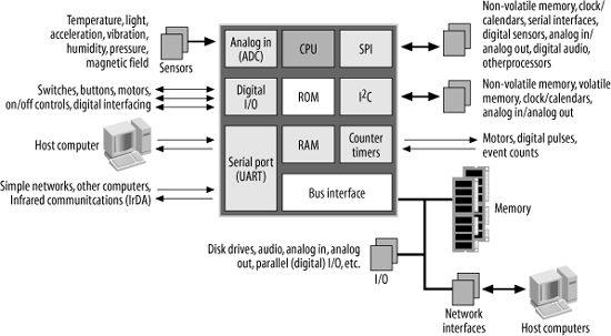
Smaller embedded systems use microcontrollers as their processor, with the advantage that this processor will incorporate much of the computer’s functionality on a single chip. An arbitrary embedded system, based on a generic microcontroller, is shown in Figure 1-12.
The microcontroller has, at a minimum, a CPU, a small amount of internal memory (ROM and/or RAM), and some form of I/O, which is implemented within a microcontroller as subsystem blocks. These subsystems provide the additional functionality for the processor and are common across many processors. The subsystems that you will typically find in microcontrollers will be discussed in the coming chapters.
For the moment, though, let’s take a quick tour and examine the purposes for which they can be used.
The most common I/O is digital I/O , commonly called general-purpose I/O , or GPIO . These are ports that may be configured by software, on a pin-by-pin basis, as either a digital input or digital output. As digital inputs, they may be used to read the state of switches or push buttons, or to read the digital status of another device. As outputs, they may be used to turn external devices on or off, or to convey status to an external device. For example, a digital output may be used to activate the control circuitry for a motor, turn a light on or off, or perhaps activate some other device such as a water valve for a garden-watering system. Used in combination, the digital inputs and outputs may be used to synthesize an interface and protocol to another chip. Most microcontrollers have other subsystems besides digital I/O but provide the ability to convert the other subsystems to general-purpose digital I/O if the functionality of the other subsystems is not required. This gives you great versatility as a system designer in how you use your microcontroller within your application.
Many microcontrollers also have analog inputs, allowing sensors to be sampled for monitoring or recording purposes. Thus, an embedded computer may measure light levels, temperature, vibration or acceleration, air or water pressure, humidity, or magnetic field, to name just some. Alternatively, the analog inputs may be used to monitor simple voltages, perhaps to ensure the reliable operation of a larger system.
Some microcontrollers have serial ports, which enable the embedded computer to be interfaced to a host computer, a modem, another embedded system, or perhaps a simple network. Specialized forms of serial interface, such as SPI and I2C, provide a simple way of expanding the microcontroller’s functionality. They allow peripherals to be interfaced to the microcontroller, providing access to such devices as off-chip memories (for data or parameter storage), clock/calendar chips (for timekeeping), sensors with digital interfaces, external analog input or output, and even audio chips and other processors. Most microcontrollers have timers and counters. These may be used to generate internal interrupts at regular intervals for multitasking, to generate external triggers for off-chip systems, or to provide control pulses for motors. Alternatively, they may be used to count external triggers (pulses) from another system. A few microcontrollers also include network interfaces, such as USB, Ethernet, or CAN. In this book, we’ll look at many of these peripheral subsystems in detail and see how to utilize them to increase an embedded computer’s functionality.
Some of the larger microcontrollers also provide a bus interface, bringing the internal address, data, and control buses to the outside world. This allows the processor to be interfaced to a huge variety of possible peripherals in very much the same way as a conventional processor. All of the possible devices and interfaces described previously may also be implemented through the bus interface and the appropriately chosen peripheral. A bus interface provides enormous possibility.
The mix of I/O subsystems that microcontrollers may have varies considerably. Some microcontrollers are intended for simple digital control and may have only digital I/O. Others may be intended for industrial applications, and may have digital I/O, analog input, motor control, and networking. The choice of microcontroller (and there are literally thousands of subspecies available from dozens of manufacturers) depends on your processing needs and your interfacing requirements. Choose the one that best suits your purposes.