Chapter 5. Power Sources
The attention span of a computer is only as long as its electrical cord.
—Turnaucka’s Law
There is one important aspect that must be included in all embedded computer designs—power. In this chapter, we look at power sources for your computer and voltage regulation to keep your power smooth and reliable.
Your embedded computer system needs electricity. You have several options when it comes to powering your system: coal, nuclear, hydro, geothermal, or batteries. The first four fall under the general category of “what comes out of the wall.”
The Stuff Out of the Wall
If your system doesn’t need to be portable, this is the most obvious choice. What comes down the “pipe” is AC and is far too high a voltage to be of immediate use to a digital system. It must be converted to a DC voltage of significantly lower magnitude. There are plenty of solutions for doing this. You can use DC “lab” power supplies, standard PC supplies (probably overkill for your needs), or AC adaptors . The last of these is probably the best choice for most applications.
AC adaptors (also known as plug packs or sometimes power bricks ) are the little black boxes that come with your cell phone and a host of other appliances. They are a cheap, easy, and reliable solution and can be purchased from any good electronics vendor. Typically, they will provide an output voltage somewhere in the range of +5 VDC to +12 VDC and can supply a current of up to a few Amps, depending on the particular plug pack. Choose one that will supply an appropriate voltage and current for your system. One caveat with plug packs is the polarity of the connector. Most plug packs have the positive voltage on the center of the connector jack and ground on the outside. Other plug packs have the exact opposite arrangement! Not knowing which you have could lead to disastrous consequences for your embedded system. As always, check the technical data and, if in doubt, use a multimeter to check the output polarity before connecting it to your system.
A better way is to incorporate a bridge rectifier as part of your design (Figure 5-1). That way, the polarity of the power source makes no difference. The input power is DC, but the polarity of the connection makes no difference. The embedded system uses the output of the rectifier as its power source and has internal voltage regulation. (We’ll discuss regulators shortly.)

Batteries
Batteries are easy to use. The only caveat is to ensure that the battery (or batteries ) you have chosen can supply enough current at the right voltage. With the right choice of battery and a carefully designed system, you can achieve extended operation over very long periods. For example, a small PIC- or AVR-based computer can (depending on application and design) operate for up to two years off a single AA battery. A poorly designed system can drain a battery in minutes. A poorly chosen battery unable to supply sufficient current will result in erratic operation, or may result in the system being unable to start at all. When choosing a battery, consider not just its average current capability but also its peak current. An embedded computer may need only an average supply of 20 mA but may require as much as 100 mA at peak loads. This is especially true of systems using flash memory, which may require high currents during write operations. The battery for such a system must be able to supply not just the continuous load, but also the peak load when required.
Low Power Design
There are several ways you can reduce the power consumption in your embedded system. The use of low-power devices is the most obvious place to start. The power consumption of different chips varies considerably, and there are many low-power variants of common devices available. RISC processors often have lower power consumption than comparable CISC processors, so they are often used in preference to CISC in low-power applications. The PIC and AVR microcontrollers can have current draws of less than 5 mA (and as low as 10 nA when in sleep mode). This is considerably less than the 35 mA used by a 68HC11 microcontroller.
Many memory chips and peripherals will automatically enter a low-power mode when they are not in use. Others may be placed in low-power mode by toggling a digital input or by an appropriate software command. The power consumption of some devices can be reduced even further by turning them off when not in use. If the processor is executing code from RAM and outputting data to a serial port, then the power to the ROMs and any other I/O devices may be turned off since they are not in use. Implementing this requires separate power sources for the chips that are to be disabled, switched via software control. Some voltage regulators (discussed in the next section) have shutdown inputs, allowing the subsystem they are powering to be turned off.
Further, some low-power devices (such as sensors) may need very little current, so little that they can be directly powered from the I/O line of a microcontroller. The I/O signal is the power supply for the device. The devices can be turned on or off under software control by toggling the I/O line. Some processors, such as the PIC and AVR, can sink relatively large currents (20 mA) through their I/O pins, and these can be used as ground for some devices (such as LEDs).
Regulators
A voltage regulator is a semiconductor device that converts an input DC voltage (usually a range of input voltages) to a fixed output DC voltage. They are used to provide a constant supply voltage within a system.
While many components in an embedded system can operate from a wide power-supply range, a fixed operating voltage is necessary for devices such as Analog-Digital Converters (ADCs), since many use the internal power supply as a reference. In other words, the output voltage of a sensor is sampled as a percentage of the voltage supply of the ADC. If the supply is not a known voltage, then any sampling performed by the ADC is meaningless. (We’ll look at ADCs and sampling in Chapter 13.) Therefore, we need a voltage regulator to provide a constant voltage source, and thereby a constant voltage reference. Further, a voltage regulator can assist in removing power-supply noise and can provide a degree of protection and isolation for the embedded system from the external power supply. If your system is operating from a battery, the varying current draw of your computer can combine with the battery’s internal resistance to create a varying supply voltage. The addition of a voltage regulator prevents this from becoming a problem since it provides a constant output. Including a voltage regulator in your design is good practice.
Tip
National Semiconductor has a good online tutorial on using and designing voltage-regulator circuits based on their chips. It can be found at http://www.national.com/appinfo/power/webench.
The types of regulators we will look at are termed DC-DC converters . They take an unregulated DC voltage (often over a range of possible voltages) and provide a constant DC voltage output of a fixed value.
There are three types of DC-DC converters: linear regulators , which produce lower voltages than the supply voltage; switching regulators that can step up (boost), step down (buck), or invert the input voltage; and charge pumps , which can also step up, step down, or invert the supply voltage, but with limited current-drive capability. (Note that not all charge pumps provide regulated voltage.)
The conversion process of any regulator is not 100% efficient. The regulator itself uses current (known as >quiescent current ), and this is sourced from the input supply. The greater the quiescent current, the more power (and therefore heat) the regulator must dissipate. In choosing a regulator, select one that can supply the appropriate output voltage and the required current needed by your embedded system, yet has the lowest quiescent current.
Linear regulators are small, cheap, low-noise, and very easy to use. The basic circuit for a linear regulator is shown in Figure 5-2. The inputs and outputs are filtered using decoupling capacitors, but beyond that, no other external components are needed.

As well as helping to smooth the voltages, the capacitors also help remove momentary glitches in the power source known as brownouts . These momentary drops in power are infrequent, but when they occur, they can severely corrupt a computer’s operation.
Tip
Many microprocessors include brownout detectors that will restart the processor if a brownout gets through to the processor’s power inputs.
Switching regulators get their name because they switch a power transistor (MOSFET) at their output. They tend to be more efficient than linear regulators in converting the input voltage to the output voltage. In other words, they waste less power during the conversion process. However, their drawback is that they require more external components (such as an inductor and diode) and therefore take up more space. They also typically cost more and generate far more noise than linear regulators. Unlike linear regulators, they can step up a voltage as well as stepping one down, and they can also invert. For example, a switching regulator can take a supply voltage of 3.6 V from a battery and provide you with a regulated 5 V supply for your embedded system. Alternatively, a switching regulator may take an unregulated 8 V supply and convert this to a regulated -12 V supply. Switching regulators are far more versatile than linear regulators. However, they do require careful design and board layout, so pay careful attention to the directions of the particular component manufacturer. As always, read the datasheets carefully.
Charge pumps, like switching regulators, can step up, step down, or invert voltages. Unlike switching regulators, they require no external inductor. However, due to their limited capacity to supply current, they are not commonly used. The MAX3222 (and similar devices), discussed in Chapter 9, use internal charge pumps to generate the +12 V and -12 V required for RS-232C level shifting.
LM78xx Regulators
There are literally thousands of voltage regulators available. Probably the most commonly used are the LM78xx linear regulator series made by several manufacturers such as Fairchild (http://www.fairchildsemi.com), Semelab (http://www.semelab.co.uk), and ST Microelectronics (http://www.st.com). They typically come in a TO-220 package (Figure 5-3) and have a metallic attachment point for a heatsink, such as the one shown in Figure 5-4. The regulator is normally mounted flat against the circuit board, and the pins are bent 90 degrees downward.
The part number designates the output voltage. For example, an LM7805 provides a 5 V regulated output, while an LM7812 gives a regulated 12 V output. They can provide an output current of up to 1 Amp (and as much as 2.2 Amps peak), with a quiescent current of between 5 mA and 8 mA. They also feature overload and short-circuit protection. Table 5-1 lists the regulators, their input voltage ranges and their output voltages.


|
Part |
Output (V) |
Input range (V) |
|
LM7805 |
5 |
7–25 |
|
LM7806 |
6 |
8–25 |
|
LM7808 |
8 |
10.5–25 |
|
LM7809 |
9 |
11.5–25 |
|
LM7810 |
10 |
12.5–25 |
|
LM7812 |
12 |
14.5–30 |
|
LM7815 |
15 |
17.5–30 |
|
LM7818 |
18 |
21–33 |
|
LM7824 |
24 |
27–38 |
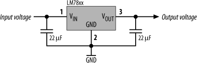
The LM78xx is simple to use. Decoupling capacitors (nominally between 10 uF and 47 uF) are required on the input (pin 1) and output (pin 3), as shown in Figure 5-5. Pin 2 is connected to ground.
For negative output voltages, use an LM79xx regulator. It’s used in exactly the same way as an LM78xx.
MAX603/MAX604 Regulators
A good small regulator is the Maxim MAX603 (5 V output) or MAX604 (3.3 V output). I tend to use these as the default “workhorse” regulators for many of my small designs. They use far less quiescent current than LM78xx regulators and as such are ideal for low-power or battery-operated systems. They are available in tiny surface-mount SO-8 or in standard DIP packages (discussed in Chapter 6) ande require only two external components.
The MAX603/604 can provide up to 500 mA of current and can operate from an input voltage of between +2.7 V and +11.5 V DC. They have built-in protection in case you inadvertently switch power and ground and consume as little as 15 μA of current for their own use. As such, they are ideal for use in low-power, embedded computers. The schematic for using a voltage regulator such as a MAX603 or a MAX604 is shown in Figure 5-6. In this case, the input supply is a battery, but it could just as easily be a DC plug pack or some other sort of supply.

A capacitor is required at the output (pin 8 of the regulator) to filter the voltage. This capacitor forms part of the regulation circuit and is required. The device will not work without it. The second support component required is a capacitor on the input (pin 1). This stabilizes the input voltage and can provide an additional current source during peak loads. These capacitors are known as decoupling capacitors and are discussed in detail later in this chapter.
Tip
Every component should have a decoupling capacitor for every powersupply pin. This is important. Leaving them off is a good way to ensure that your computer will be unreliable.
The ground pins (2, 3, 5, 6, and 7) should all be connected to ground, as they act as a small heatsink for the device. When laying out the PCB, place a ground fill under the regulator and connect these five pins directly to it. Pin 4 (![]() ) places the regulator in shutdown mode. For constant operation, this pin is connected directly to the power source, such that the device is always on. If you’re using this regulator to power a subsystem within your embedded computer, you can use
) places the regulator in shutdown mode. For constant operation, this pin is connected directly to the power source, such that the device is always on. If you’re using this regulator to power a subsystem within your embedded computer, you can use ![]() to act as a software-controlled power switch by connecting it to an I/O line of the processor.
to act as a software-controlled power switch by connecting it to an I/O line of the processor.
A MAX604 gives a regulated 3.3 V output. For a 5 V output, replace the MAX604 with a MAX603. The circuit is otherwise the same.
MAX1615 Regulator
The MAX1615 is a linear regulator that can operate from a supply range between 4 V and 28 V. It is tiny and is capable of supplying 30 mA of output current at either 3.3 V or 5 V. 30 mA is not much current, but for very small (battery-powered) applications, it may be sufficient. The MAX1615 has a shutdown input, allowing an external system to power it down. One use for this regulator could be as a power source to subsystems within an embedded computer, allowing the host processor to turn them off when not in use. Before turning off a subsystem, ensure that its “absence” won’t adversely affect the functionality of the rest of the system.
The basic schematic for a MAX1615 circuit is shown in Figure 5-7.

The 5/
![]() pin determines the output voltage. By tying it to ground, the output is set to 3.3 V. Connect the pin to the input, and the output voltage is set to 5 V. For continuous operation, tie the shutdown pin (
pin determines the output voltage. By tying it to ground, the output is set to 3.3 V. Connect the pin to the input, and the output voltage is set to 5 V. For continuous operation, tie the shutdown pin (![]() ) to the input voltage. To allow the regulator to be powered down, connect
) to the input voltage. To allow the regulator to be powered down, connect ![]() to a processor I/O line or a simple power switch. (It goes without saying that if you’re driving
to a processor I/O line or a simple power switch. (It goes without saying that if you’re driving ![]() with an I/O line of the processor, then that processor must have a power source other than this regulator! Otherwise, it could lead to some interesting situations.)
with an I/O line of the processor, then that processor must have a power source other than this regulator! Otherwise, it could lead to some interesting situations.)
MAX724 Regulator
For higher-current situations, the MAX724 can supply up to 5 A from an input supply voltage between 8 V and 40 V. Its output is adjustable from 2.5 V to 35 V, and its quiescent current is 8.5 mA. It comes in a 5-pin TO-220 package, with an attachment point for an external heatsink. The basic circuit for a MAX724 is shown in Figure 5-8. Note that it is a step-down regulator only.

The inductor is nominally 50 uH, but can be any value in the range of 5 uH to 200 uH. When the output pin VSW turns off, the diode provides a path to ground for the inductor current. The inductor chosen should have a high saturation current. If it doesn’t, the effects will be disastrous. The Maxim datasheet provides detailed information on selecting an appropriate inductor.
It is recommended by Maxim that a Schottky diode, such as an MBR745, be used due to the fast switching times required. Both the regulator’s input and output require large decoupling capacitors to filter out ripple. The capacitors must have low ESR (Equivalent Series Resistance) over the expected temperature range and operating lifetime.
The output voltage is set by resistors R1 and R2. The equation for calculating the output voltage is:
VOUT = 2.21 * (R1 + R2) / R2
R2 should be less than 4 kΩ. Maxim recommends choosing 2.21 kΩ for R2, as it simplifies the above equation:
VOUT = (R1 + 2.21k) / 1000
So, the equation to calculate R1 becomes:
R1 = 1000 * VOUT - 2.21k
The regulators I’ve covered so far should be useful in most situations. If you’re designing a machine with special requirements, there is bound to be a regulator that will suit your needs. Just spend some time browsing component manufacturers’ web sites and see what is offered.
Electrical Noise and Interference
Digital systems are inherently analog in operation. Digital signals suffer degradation and noise due to analog effects present in the system. Spurious noise or reflections from nearby electrical machinery or radio transmissions can induce signals within your circuit that can cause false events to occur, or even prevent a digital system from functioning at all. The one way to ensure that your system is immune to electromagnetic interference is to avoid the use of electricity! Unfortunately, the steam-powered microprocessor is not a reality, so if your system is to operate reliably in the real world, you must take electromagnetic effects into account. What follows is not a comprehensive overview of noise and associated problems and solutions, which is far too complex a field to cover properly here. What I will do is provide an introduction. It is worth seeking out information that is more detailed to understand these concepts more thoroughly.
Warning
The United States, Australia, the European Union, and many other countries have very strict guidelines and requirements for electromagnetic emission and immunity. The recommendations presented here are good practice only and are not necessarily sufficient to warrant compliance in your country. Therefore, it is important that you check your local regulations and ensure that you meet the appropriate requirements. Compliance cannot be guaranteed just by design. A system must be tested to ensure that it is compliant.
Noise can be a significant problem in digital systems. Noise can disturb signal transmission, leading to corrupted data, or may even cause a program to crash. Problems with an embedded system may or may not be noise-related. Similar problems can also be caused by inadequate power-supply levels, insufficient decoupling capacitors, marginal timing tolerances, and software bugs. However, even a well-conceived system can be disrupted by noise. There may be noise problems inherent in the design. Switching noise from integrated circuits, ringing, and crosstalk (discussed shortly) are all due to aspects of the designed system. Other forms of noise may be due to environmental effects (such as nearby motors or radio emissions). The bad news is that electromagnetic problems are getting worse for digital systems. The environment is bathed in ever-increasing emissions from radio, TV, and cell-phone towers. At the same time, integrated circuits are becoming increasingly sensitive, as designs move towards higher-speed and lower-power operation.
These sources of noise may not be present during the design and test phase of the system but will only manifest themselves once the system is out “in the field” and in service. A crashed embedded system may be due to a hardware problem, a software problem, or the fact that the factory a block away turned on a compressor, which caused a spike on the power supply. Field problems created by noise may only occur very occasionally and can often be very difficult to track down. It is not unusual for some problems to occur only once every few days. Any problem is not satisfactory and must be fixed, but identifying the cause is not always easy. It is better to design the system from the beginning to be as immune to these problems as possible. You have to consider not just what emissions your system may produce, but also how it may be susceptible to external effects. This will not guarantee your system will be problem-free, but every bit of immunity helps.
Electromagnetic interference (EMI) is noise generated by sources external to the embedded system. Some examples of EMI are motors, switches in power consumption, fluorescent lighting, RF emissions, and electrostatic discharges. All can be significant sources of noise. For example, turning on or off a machine with an electric motor can cause a 1000 V spike on the AC power-supply line. An electrostatic discharge (ESD) can send a spike of 35 kV from a finger into an integrated circuit with a current rise time of 4 Amps per second! This can be enough to permanently damage a sensitive chip. Cars are particularly noisy environments. The 12 V supply line to the automotive electronics may be reversed, driven at voltages ranging from 6 V to as much as 24 V, and have ± 400 V transient spikes. All of these can have very adverse effects on the operation of an embedded system.
In any circuit, there is a wire carrying current in and a wire carrying current out. Current flowing through a wire generates a magnetic field around that wire. Such a magnetic field can be a source of EMI. The intensity of the magnetic field felt is inversely proportional to the distance from the source of the field, and the orientation of the field relates directly to the direction of current flow in the wire.
Minimize the Current Loop Area
Current flows through a system via the power and signal connections and back to the power supply (thereby completing the circuit) through ground. Ground thus forms the return path for current flowing within the system. If the signal wire and return wire are located close together, the magnetic fields generated by the currents in the wires cancel out within a short distance of the wires. The objective is to keep all signal and return paths as close together and as short as possible. This is known as minimizing the current-loop area . Where there are many current loops present in a system (as is common in many large, high-speed, digital systems), a ground plane is used to minimize loop area. A ground plane is a large conducting surface that can serve as the current return path for all loops in the circuit. A ground plane is often implemented as a complete, internal PCB layer.
Capacitive coupling is the coupling of electric fields. A signal on one wire, through its associated electric field, can capacitively induce a phantom “signal” in an adjacent signal line. This is known as crosstalk in digital systems. If not designed correctly, the magnitude of the crosstalk in a system can be significant and can easily cause a crash.
Capacitive coupling may be reduced by shielding the signal lines with an electrostatic or Faraday shield . This shield is a metal conductor placed between the capacitively coupled elements. The shield is simply part of the PCB (discussed in Chapter 6), formed in the same way as the circuit tracks, and is usually grounded (though not always). The shield may be a simple ground plane under an integrated circuit to protect it from signal lines on the underside of the circuit board. Signal lines may be shielded from each other (if necessary) by placing a ground line between them.
Keep the Power Smooth
The principle of keeping current loops small applies as much to power lines within a system as it does to signal lines. However, keeping the loop area small for power is difficult. Power must be distributed throughout the circuit, and to effectively route this throughout a PCB, and keep the loop area small, is very difficult. The power lines can therefore be susceptible to noise, and this can cause major problems to the circuit.
The solution is to provide a path to ground for any noise present in the power supply. This should be done locally for each component in the circuit. It is achieved by adding a decoupling capacitor between power and ground for each integrated circuit. The capacitor decouples the noise from the power source and provides a path to ground for it. In this way, noise is removed from the power supply, and the chips have a constant and clean voltage source. The decoupling capacitors should be placed as close as possible to the power pins of the devices. Surface-mount capacitors have very low inductance connections, and so are preferable. Ceramic capacitors are normally used for decoupling capacitors due to their low resistance.
The capacitor has the added advantage of acting as a current source for the device when the device must switch its outputs or internal state. As such, it represents a current source with a much smaller loop area. Generally, the circuit board will be decoupled by a large (22-100 uF, say) electrolytic or tantalum capacitor placed near the power input, and each integrated circuit will be separately decoupled by 10 nF ceramic capacitors. Multiple decoupling capacitors, one for each power pin, improve the situation. You need to ensure that all frequencies that may affect the circuit have a low impedance path to ground. To this end, several capacitors (100 nF, 10 nF, and 100 pF) can be used to decouple a wide range of frequencies and thereby remove noise from the power-supply circuits. You can never have enough decoupling capacitors (within reason). Additionally, an onboard voltage regulator can provide a degree of isolation between your circuit and the external power supply.
Noise can also be present in ground lines. Ground is not always at the same potential in all locations. There can be a voltage difference between the local grounds in different parts of a circuit that are both connected to “ground.” In some instances, this voltage difference can drive currents of several Amps through the ground line. This is referred to as a ground loop , and can result in serious problems. Shielding, decoupling, and minimizing the current-loop area can help protect against ground noise.
Ground bounce is ringing (oscillation) on signal lines caused when one or more outputs on the same device are being switched from high to low. This ringing can be of significant amplitude and can adversely affect the system. Some devices are designed so that ground-bounce effects are minimized. Using devices in packages with shorter leads (such as PLCC and surface-mount) can reduce ringing effects. Devices with ground and power pins toward the center of the package have shorter lead lengths, and this also helps to reduce ringing effects. Termination techniques can also help to reduce ground bounce .
Another effect you are likely to encounter is caused by the simultaneous switching of several outputs at once. Like ground bounce, it is due to parasitic effects relating to packaging and internal wiring of the chips. When several outputs switch at once, these effects can cause a delay of several nanoseconds in the changing output signals. Component datasheets usually specify timing parameters for a single changing output. You need to consider the effect that several changing outputs may have on your circuit.
How to Destroy a Computer Without Really Trying
Walk across a carpet on a dry day, or rub a cat against some plastic, and a static charge will build up. If you or the cat then touches something metallic, the jolt you both feel is an electrostatic discharge (ESD ). An ESD can destroy an integrated circuit permanently. The ESD may be too small to be felt, but it can still send a semiconductor to that great beach in the sky.
Many integrated circuits have internal protection against ESD. Semiconductor manufacturers, such as Maxim, are now building protection into their devices that can withstand ESDs of 15 kV or more. This protection is sufficient to safeguard the device against the charge build-up that can occur during normal handling. It is not, however, sufficient to protect the device against the huge electrostatic sparks that can sometimes occur. Once a device is in-circuit, it should not be considered safe. It is possible for a processor to be destroyed by a spark received when a typist puts fingers on a keyboard. The spark, like a lightning strike, will attempt to find a path to ground, even if that means traveling down a data line and through the processor to get there.
One solution is to include a buffer chip to isolate the important components in the system from those that may come in contact with an ESD. This is not an ideal solution. It simply means that the buffer will be destroyed instead of the processor. You still have a system that has failed.
Transient suppressors are available that can provide protection. Such suppressors act as an open circuit at normal voltage levels, but conduct power to ground at higher voltages. At no time should a signal ground be used to earth an ESD. Most integrated circuits don’t respond very well to having their ground pins raised to several hundred volts above their power supply by an ESD!
When handling chips, it’s a good idea to use a grounding mat . This is a conductive sheet that you connect to the ground of a handy power supply. You then wear a grounding strap around your arm, connecting you to the grounding mat. Thus, any electrostatic charge is dissipated and never gets the chance to build up.
Warning
If you’re using a grounding mat, don’t forget to take your embedded system off it before powering up. The grounding mat is conductive, and powering up a system while it is in contact with the mat can be disastrous!
In the next chapter, we’ll investigate the process of designing and building a physical computer. We’ll look at how you need to consider the electrical environment in which your system will be operating, and then we’ll go on to see how you lay out a printed-circuit board.