
Couplers, hybrids and directional couplers
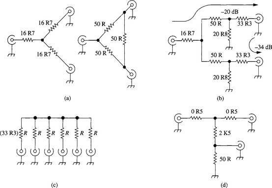
This chapter describes some further important passive components. Hybrids are based upon transformer action, whilst directional couplers depend upon capacitive coupling in addition. First a look at simple resistive couplers or ‘splitters’. These can be used to split a signal between two outputs, in any desired ratio. Figure 5.1a shows three-way resistive splitters which provide a 50 Ω match at each port, provided that the other ports are correctly matched. Any port can be used as the input and the outputs at the other two are each 6 dB down on the input and both are in phase with it. There is thus 3 dB more attenuation at each output than with an ideal hybrid coupler, which has no internal losses. There is also only 6 dB of isolation between the two output ports, but against these disadvantages resistive splitters/combiners are cheap and operate from dc to microwave frequencies. If additional loss from input to output can be accepted, the isolation between outputs increases faster than the through loss. Thus in Figure 5.1b, the loss from port A to B (or C) is 20 dB, but the isolation between ports B and C is 34 dB. Other designs (such as 10 dB through with 14 dB isolation) are simply designed by adding T pads to ports B and C of the basic 6 dB splitter of Figure 5.1a (4 dB in this case), and then combining the series resistors. The pad of Figure 5.1b is useful for combining two signals without them intermodulating, by maintaining high isolation between them, e.g. audio tones for two-tone transmitter testing, or two RF signals for intermodulation tests. Symmetrical pads with any number of ways are easily designed. Figure 5.1c shows a six-port 50 Ωsplitter, the loss from an input to any output being 14 dB. Such multiport couplers are useful for hardwired signal-path testing of a radiocommunications net with N transceivers. Where two unequal outputs are required, the through loss to the greater of the two outputs can be less than 6 dB. Figure 5.1d shows a resistive divider for use as a ‘signal sniffer’, e.g. to sample the output of a transmitter for application to a spectrum analyser. The output at port C is 40 dB down on that at port B. The loss from port A to B is less than 0.2 dB. In practice, the two 0.5 Ω resistors would probably be omitted. The design of asymmetric dividers for splitting losses which differ by only a few decibels is tedious; if 6 dB attenuation is acceptable in the main path then it is simpler to add a pad giving the required difference in attenuation to the output of a Figure 5.1a type splitter.
A hybrid can divide the input signal power between two outputs with negligible loss, each output being 3 dB down on the input. The basic hybrid circuit is shown in Figure 5.2a. If a signal is applied at port A, it will be divided equally between ports B and C whilst no power is delivered to port D (which could therefore be loaded with any termination from a short to an open circuit) as can be seen from the symmetry of the circuit, given that ports B and C are both terminated in 50 Ω. The outputs at ports B and C are in antiphase and the arrangement is known as a 180° hybrid (port D is often terminated internally in 25 Ω and only ports A, B and C made available to the user). The corollary is that if two identical signals of equal amplitude but 180° out of phase are applied to ports B and C, all of the available power is combined and delivered to port A, port D again being isolated. If, however, the two identical signals were in phase (Figure 5.2b), the currents in the centre tapped winding would produce no net flux on the core, so that port A is isolated and all the power is delivered to port D. If this is terminated with a 25 Ω load, then since ports B and C each supply half of the power, each will ‘see’ a 50 Ω termination. The corollary is that if a signal is applied at port D, it will be divided equally between ports B and C, the outputs being in phase, with port A isolated. This arrangement is known as a 0° hybrid: port A may be terminated internally in 50 Ω and an autotransformer is usually fitted to transform port D to 50 Ω. The 180° hybrid is cheaper as an autotransformer is not needed. Sometimes all four ports are brought out, giving a ‘sum and difference hybrid’.
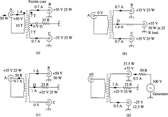
Figure 5.2c shows what happens if a signal is applied to port B. The input power divides equally between port A and ‘port D’ - a 25 Ω resistor in the case of a 180° hybrid - with port C isolated. The split between ports A and D is almost perfect, the small difference component of current required to supply the magnetizing flux on the core being in quadrature.
Thus for a correctly terminated four port hybrid, the power always splits equally between ports adjacent to the input port, the opposite port being isolated. Figure 5.2d shows what happens if one of the adjacent ports is mismatched - here port A is open circuit. A current of 0.5 A flows into port B and the currents at ports C and D can only be as shown, since there must be ampere-turn balance in the centretapped winding. So the output voltages and powers at ports B and D can be marked in. A total of 37.5 W is supplied to port B, and the voltage there is 75 V: the source sees a load of 150 Ω instead of the designed load of 50 Ω. Note that even for this extreme mismatch of one adjacent port, the power in the other is totally unaffected, and still twice that in the ‘isolated’ port: if the mismatch at adjacent ports is small, a hybrid provides high isolation at the fourth port. Most importantly, the fact is that opencircuiting (or short-circuiting) port A has no effect whatever on the power delivered by port B to port D, indicating perfect mutual isolation between the two opposite ports adjacent to the input port (if and only if the source impedance is an ideal 50 Ω).
A five-port hybrid divides power equally between four output ports, maintaining high isolation between them. It consists of two hybrids connected to opposite outputs of a third Figure 5.2a type hybrid and can equally well be used to combine the power outputs of, say, four amplifier stages in a solid state transmitter. Usually the difference ports of the three constituent hybrids are terminated internally. Further levels of buildup can provide 8- or 16-way couplers, etc. Occasionally the number of ways required is not a power of two. Figure 5.3 shows a hybrid which splits the input power three ways.
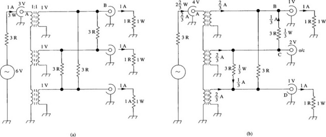
Figure 5.3 Three-output hybrid (Normalized to 3 Ω in, 1 Ω out to illustrate operation. For a 50 Ω hybrid at all ports, transformer ratios are each 4:7)
It is instructive to work out what happens if one of the output ports is mismatched, port C open circuit for example. Remember that as the primaries of the three transformers are in series, the secondary currents cannot differ substantially, but that as the magnetizing current is small (and in quadrature), the primary voltages can differ. It turns out that on open circuiting port C, the outputs at ports B and D are unchanged, but that in each case one-third of the current is provided via one of the resistors from the centre transformer. Furthermore the load seen by the generator rises to 2Z, the power supplied by it falls by 1/9th and the voltage at the input port rises by a third. Full marks if your analysis comes up with these results: hint, the secondary voltage of the centre transformer doubles. Figures 5.2 and 5.3 together enable low-loss high-isolation splitting or combining arrangements for 2, 3, 4, 6, 8 or 9 outputs. A five-way split can be achieved rather like Figure 5.3 but using five transformers with primaries in series: a terminating resistor is required between each possible pair of secondary outputs. The arrangement is unwieldy and even more so for seven or more ways. So for a seven-way split, it is usually better to use an eight-output hybrid and simply terminate off the unused output. For combining, e.g. of transmitter modules, it is better to design around a power of two (and/or three) modules from the outset.
The coupler of Figure 5.1d could be used to obtain a low level sample of a high power signal, e.g. for measurement purposes. The same output at port C results whether the power in the ‘main line’ flows from port A to B or vice versa. In a directional coupler the transfer of power from one port to another is dependent upon the direction of power in the main line. The operation of one type is as follows (see Figure 5.4a). Power from a source, e.g. a transmitter, flows through the primary of a current transformer L1, e.g. to a (hopefully) matched antenna presenting a 50 O load. It is important to note that the reactance of L1 is very low compared to 50 O so that the current flowing is determined solely by the power available from the source and the impedance of the load. Imagine for the moment a 50 O source and that the load is a short circuit: then the current flowing will induce a quadrature voltage in L2 proportional to the rate of change of the current. Half of the voltage will appear at A and the other half at B, in antiphase, since the two earthed resistors R are equal and form a balanced bridge. The capacitor C will have no effect, as there is no voltage at the centre tap of L2, nor at L1 due to the shorted load. Now imagine the load is open circuit: no current flows through L1 so no voltage is induced in L2, so points A and B must be at the same potential. The voltage on the main line will force a leading (capacitive) current through C, whose reactance is much higher than R. Suppose C has been selected so that the voltage produced at A is the same as when the load was short circuited. Now, when a matched load is connected, the components of voltage at A due to inductive and capacitive coupling will add, while those at B will cancel out. If the direction of flow of power in the main line were reversed, the voltages at B would add and there would be no voltage at A. With any value of load, the voltage at A is proportional to the forward power and that at B to the reverse power, so if diode detectors are connected at A and B, we have a means of monitoring the forward power supplied by the source and reverse power reflected by a mismatched load, e.g. for purposes of measurement and control in a transmitter. As the frequency of operation is raised, both the current-induced and the capacitively-coupled voltages will rise pro rata. Consequently the detected voltages will rise, but the directivity is maintained.
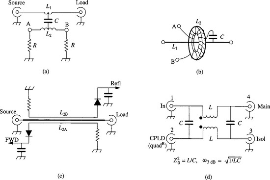
The construction of a directional coupler can take many forms: in Figure 5.4b a toroidal core surrounding the main line (a single turn primary) is used. In Figure 5.4c separate lines L2A and L2B are used as secondaries to monitor forward and reverse power separately. The dimensions and spacings of the three lines are chosen to give the appropriate ratio of capacitive to inductive coupling. It is important that the coupled lines are short compared to a wavelength, so that the capacitive coupling can be considered as a lumped component. This results in the signal coupled into the measuring circuit being only a tiny fraction of the through energy, a limitation which is quite acceptable, indeed desirable, in this application. When two lines are close spaced over an appreciable fraction of a wavelength, much tighter coupling can be achieved. If the lines are one quarter of a wavelength long at the operating frequency, a 3 dB split of power between the main and coupled lines can be achieved, the main and coupled outputs being in quadrature. This technique is conveniently implemented at UHF using ‘microstrip’ or ‘stripline’ lines. A microstrip line consists of a track on a printed circuit board (the other side of which is covered in copper ground plane), the width required to give a 50 Ω impedance depending upon the thickness and dielectric constant of the PCB material [1, 2]. Stripline is similar but covered with a second PCB carrying just a copper ground plane. Using this technique, quadrature couplers operating at frequencies as low as VHF are available, the coupled lines being ‘meandered’ on the surface of the PCB, for compactness. Bandwidth is typically 10° for ±0.6 dB variation in amplitude between the main and quadrature outputs. More complicated structures offer quadrature couplers with 11/2 octave bandwidth [3] whilst quadrature couplers covering 2-32 MHz have been designed by Merrimac. At these frequencies, quadrature couplers use lumped components, the basic narrow-band section being as in Figure 5.4d. The two inductors L are wound using bifilar wire to give 100% coupling, and Figure 5.4d gives the component values in terms of the design impedance level and centre frequency.
Circulators and isolators are examples of directional couplers, and are common enough components at microwave frequencies. They are three port devices, the ports being either coaxial- or waveguide-connectors, according to the frequency and particular design. The clever part is the way signals are routed from one port to the next, always in the same direction. The operation of a microwave circulator (or isolator) depends upon the interaction, within a lump of ferrite, of the RF field due to the signal, and a steady dc field provided by a permanent magnet, to do with the precession of electron orbits. Microwave circulators are narrow band devices, although types with up to an octave bandwidth are available. However, these have limited ‘directivity’, typically only 20 dB or less.
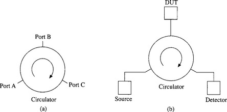
Figure 5.5a shows (diagrammatically) a three port circulator, the arrow indicating the direction of circulation. A signal input at any port appears unattenuated at the next port round, the device having (ideally) perfect three way symmetry. This means that a signal applied at port A is all delivered to port B, with little (ideally none, if the device’s directivity is perfect) coming out of port C. What happens next depends upon what is connected to port B. If this port is terminated with an ideal resistive load equal to the device’s characteristic impedance (usually 50 Ω in the case of a circulator with coaxial connectors), then all of the signal is accepted by the termination and none is returned to port B - the ‘return loss’ in dB is infinity. But if the termination on port B differs from (50 + j0) Ω, then there is a finite return loss. The reflected (returned) signal goes back into port B and circulates around in the direction of the arrow, coming out at port C. Thus the magnitude of the signal appearing at port C, relative to the magnitude of the input applied to port A is a measure of the degree of mismatch at port B. Thus with the aid of a source and detector, a circulator can be used to measure the return loss - and hence the VSWR - of any given DUT (device under test), as in Figure 5.5b. This rather assumes that the detector presents a good match to port C. Otherwise it will reflect some of the signal it receives, back into port C of the circulator - whence it will resurface round the houses at port A. So for this application, an isolator would be more appropriate. This is similar to a circulator, except that there is no coupling between ports B and C.
Given a total mismatch (a short or open at port B), then all of the power input at port A will come out at port C (but strictly via the clockwise route) - bar the usual small insertion loss to be expected of any practical device.
Microwave circulators with high directivity are narrow band devices. Circulators and isolators are such useful devices, that it would be great if economical models with good directivity were available at UHF, VHF and even lower frequencies, and even better if one really broadband model were available covering all these frequencies at once. Though not as well known as it deserves, such an arrangement is in fact possible. I first came across it in the American controlled circulation magazine RF Design [4]. This circuit uses three CLC406 current feedback opamps (from Comlinear, now part of National Semiconductors), and operates up to well over 100 MHz, the upper limit being set by the frequency at which the opamps begin to flag unduly. The article describes an active circuit switchable for use as either a circulator or an isolator, as required. It has three 50 Ω BNC ports, and operates from - say − 200 MHz, right down to dc. The circuit is shown in Figure 5.6.
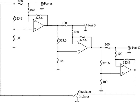
Figure 5.6 The circuit of the active circulator/isolator described in Ref. 4
Whilst at the leading edge of technology when introduced, and still a good opamp today, the CLC 406 has nonetheless been overtaken, performance-wise, by newer devices such as the AD8009 from Analog Devices. These could simply be substituted for the CLC 406 in the circuit of Figure 5.6. However, using the AD8009, after some experiment, I developed an isolator usable from dc up to 500 MHz [5].
References
1. pp. 29–34 Tam, A. Principles of Microstrip Design, RF Design. (With further useful references), 1988. (With further useful references)
2. Matthei, Young, Jones. Microwave Filters, Impedance Matching Networks and Coupling Structures. McGraw-Hill: 1964.
3. pp. 58–61, Ho, C.Y. Design of Wideband Quadrature Couplers for UHF/VHF, RF Design. (With further useful references), 1989. (With further useful references)
4. Wenzel, C. Low Frequency Circulator/Isolator Uses No Ferrite or Magnet, RF Design (The winning entry in the 1991 RF Design Awards Contest)
5. pp. 214–19, Hickman, I. Wideband Isolator, Electronics World. March, 1998. Reproduced in. Ian, Hickman, Analog Circuits Cookbook, 2nd Edition, Butterworth-Heinemann, 1999, 0 7506 4234 3.