
Active components for RF uses
The simplest semiconductor active device for RF applications is the diode, which like its thermionic forebear conducts current in one direction only. Arguably, semiconductor diodes are not active devices, simply non-linear passive ones, but their mode of operation is so closely linked with that of the transistor that they are usually considered together. The earliest semiconductor diode was of the point contact variety - the user-adjusted crystal and cat’s whisker used in the early days of wireless. Later, new techniques and materials were developed, enabling robust pre-adjusted point contact diodes useful at radar frequencies to be produced. Germanium point contact diodes are still produced and are useful where a diode with low forward voltage drop at currents of a milliampere or so, combined with low reverse capacitance, is required. However, for the last 30 years, silicon has been the preferred material for semiconductor manufacture for both diodes and transistors, whilst point contact construction gave way to junction technology even earlier. Figure 6.1a shows the I/V characteristics of practical diodes. Silicon is one of the substances which exists in a crystalline form with a cubic lattice. When purified and grown from the melt as a single crystal, it is called intrinsic silicon and is a poor conductor of electricity, at least at room temperature. However, if a few of the silicon atoms in the atomic lattice are replaced by atoms of a pentavalent substance such as phosphorus (which has five valence electrons in its outer shell, unlike the four electrons of quadravalent silicon), then there are spare electrons with no corresponding electron in an adjacent atom with which to form a bond pair. These spare electrons can move around in the semiconductor lattice, rather like the electrons in a metallic semiconductor, though the conductivity of the material is lower than that of a metal, where every single atom provides a free electron. The higher the ‘doping level’, the more free electrons and the higher the conductivity of the material, which is described as N type, indicating that the flow of current is due to negative carriers, i.e. electrons. P type silicon is obtained by doping the monocrystalline silicon lattice with a sprinking of trivalent atoms such as boron. Where one of these exists in the lattice next to a silicon atom, the latter has one of its four outer valence electrons ‘unpaired’- a state of affairs described as a hole. If this hole is filled by an electron from a silicon atom to the right, then whilst the electron has moved to the left, the hole has effectively moved to the right. It turns out that spare electrons in N type silicon are more mobile than holes in P type, which explains why very high frequency transistors are more easily made as NPN types.
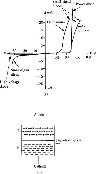
Figure 6.1b shows diagrammatically the construction of a silicon diode, indicating the lack of carriers (called a depletion layer) in the immediate vicinity of the junction. Here, the electrons from the N region have been attracted across to fill holes in the P region. This disturbance of the uniform charge pattern that should exist throughout the N and P regions represents a potential barrier which prevents further electrons migrating across to the P region. When the diode is reverse biased, the depletion layer simply becomes more extensive. The associated redistribution of charge represents a transient charging current, so that a reverse biased diode is inherently capacitive. If a forward bias voltage large enough to overcome the potential barrier is applied to the junction, about 0.6 V in the case of silicon, then a forward current will flow. The incremental or slope resistance rd of a forward biased diode at room temperature is given approximately by 25/Ia Ω, where the current through the diode Ia is in milliamperes. Hence the incremental resistance at 10 μA is 2K5, at 0.1 mA is 250 Ω and so on, but bottoming out in the case of a small-signal diode at a few ohms, where the bulk resistance of the semiconductor material and the resistance of leads, bond pads, etc., comes to predominate.
The varactor diode or varicap is a diode designed solely for reversed biased use. A special doping profile giving an abrupt or ‘hyperabrupt’ junction is used. This results in a diode whose reverse capacitance varies widely according to the magnitude of the reverse bias. The capacitance is specified at two voltages, e.g. 1V and 15 V and may provide a capacitance ratio of 2:1 or 3:1 for diodes intended for use at UHF up to 30:1 for types intended for tuning in AM radios. In these applications, the peak-to-peak amplitude of the RF voltage applied to the diode is small compared with the reverse bias voltage, even at minimum bias where the capacitance is maximum. So the diode behaves like a normal mechanical variable capacitor, except that the capacitance is controlled by the reverse bias voltage rather than by a rotary shaft. Tuning varactors are designed to have a low series loss rs, so that they exhibit a high quality factor Q over the recommended range of operating frequencies. Another use for varactors is as frequency multipliers. If an RF voltage with a peak-to-peak amplitude of several or many volts is applied to a reverse biased diode, its capacitance will vary in sympathy with the instantaneous RF voltage. Thus the device is behaving as a non-linear capacitor, and as a result the RF current through it will contain harmonic components which can be extracted by suitable filtering. A non-linear resistance would also generate harmonics, but the varactor has the advantage over a non-linear resistor of not dissipating any of the drive energy.
The P type/Intrinsic/N type or PIN diode is a PN junction diode, but fabricated with a third region of intrinsic (undoped) silicon between the P and N regions. When forward biased by a direct current it can pass RF signals without distortion, down to some minimum frequency set by the lifetime of the carriers, holes and electrons, in the intrinsic region. As the forward current is reduced, the resistance to the flow of the RF signal is increased, but it does not vary over a half cycle of the signal frequency. As the direct current is reduced to zero the resistance rises towards infinity: when the diode is reverse biased only a very small amount of RF current can flow, via the diode’s reverse capacitance. The construction ensures that this is very small, so that the PIN diode can be used as an electronically controlled RF switch or relay. It can also be used as a variable resistor or attenuator, by adjusting the amount of forward bias current. An ordinary PN diode can also be used as an RF switch, but it is necessary to ensure that the peak RF current, when on, is smaller than the direct current, otherwise waveform distortion will occur. It is the long ‘lifetime’(defined as the average length of time taken for holes and electrons in the intrinsic region to meet up and recombine, so cancelling each other out) which enables the PIN diode to operate as an adjustable linear resistor, even when the peaks of the RF current exceed the direct current.
When a PN diode which has been carrying direct current in the forward direction is suddenly reverse biased, the current does not cease instantaneously. The charge has first to redistribute itself to re-establish the depletion layer. Thus for a very brief period, the reverse current flow is much greater than the steady state reverse leakage current. The more rapidly the diode is reverse biased, the more rapidly the charge is extracted and the larger the transient reverse current. Snap-off diodes are designed so that the end of the reverse recovery pulse is very abrupt, rather than the tailing off observed in ordinary PN junction diodes. It is thus possible to produce very short sharp current pulses which can be used for a number of applications, such as high order harmonic generation (turning a VHF or UHF drive current into a microwave signal) or operating the sampling gate in a sampling oscilloscope.
Small-signal Schottky or ‘hot carrier’ diodes operate by a fundamentally different form of forward conduction. As a result of this, there is virtually no stored charge to be recovered when they are reverse biased, enabling them to operate efficiently as detectors or rectifiers at very high frequencies. Zener diodes conduct in the forward direction like any other diode, but they also conduct in the reverse direction and this is how they are usually used. At low reverse voltages a zener diode conducts only a small leakage current, like any other diode, but when the voltage reaches the nominal zener voltage the diode current increases rapidly, exhibiting a low incremental resistance. Diodes with a low breakdown voltage - up to about 4 V - operate in true zener breakdown: this conduction mechanism exhibits a small negative temperature coefficient (‘tempco’). Higher voltage diodes rated at 6 V or more operate by a different mechanism, called avalanche breakdown, which has a small positive tempco. In diodes rated at about 5 V, both mechanisms occur, resulting in a very low or zero tempco. However, the lowest slope resistance is found in diodes rated at about 7 V. Zener diodes can be used to stabilize the dc operating conditions in an RF power amplifier. Zener diodes can also usefully be employed as RF noise sources and a very few are actually specified for this purpose. It is necessary to select a diode where the noise output level is reasonably independent of frequency over the desired operating range, and stable also with respect to operating current, temperature and life. Suitable diodes can provide a useful output (say 10 to 15 dB above thermal) up to 1 GHz.
Like diodes, bipolar transistors first appeared as point contact types, though all current production is of junction devices. However, the point contact structure is preserved to this day in the symbol for a transistor (Figure 6.2a). Figure 6.2b shows diagrammatically the structure of an NPN bipolar transistor: it has three separate regions. With the base (a term dating from point contact days) short circuited to the emitter, no current can flow in the collector, since the collector/base junction is a reverse biased diode, complete with depletion layer as shown. The higher the reverse voltage, the wider the depletion layer, which is found mainly on the collector side of the junction as the collector is more lightly doped than the base. In fact, the pentavalent atoms which make the collector N type are found also in the base region. The base is a layer which has been converted to P type by substituting so many trivalent (hole donating) atoms into the silicon lattice, e.g. by diffusion or ion bombardment, as to swamp the effect of the pentavalent atoms. So holes are the majority carriers in the base region, just as electrons are in the collector and emitter regions. The collector junction then turns out to be largely notional: it is simply that plane on the one side (base) of which holes predominate whilst on the other (collector) electrons predominate. Figure 6.2c shows what happens when the base emitter junction is forward biased. Electrons flow from the emitter into the base region and simultaneously holes flow from the base into the emitter. The latter play no useful part in transistor action: they contribute to the base current but not to the collector current. Their effect is minimized by doping the emitter a hundred times (or more) more heavily than the base, so that the vast majority of the carriers traversing the base/emitter junction consists of electrons flowing from the emitter into the base. Some of these electrons combine with holes in the base and some flow out of the base, forming the greater part of the base current. Most of them, being minority carriers (electrons in what should be a P type region) are swept across the collector junction by the electric field existing across the depletion layer. This is illustrated in diagrammatic form in Figure 6.2c, while Figure 6.2d shows the collector characteristics of a small-signal NPN transistor. It can be seen that for small values of base (and collector) current, the collector voltage has little effect upon the amount of current flowing, at least for collector/emitter voltages greater than about +1.5 V. For this reason, the transistor is often described as having a ‘pentode like’ output characteristic (the pentode valve has a very high anode slope resistance). This is a fair analogy as far as the collector circuit is concerned, but there the similarity ends. The pentode’s control grid has a high input impedance whereas the emitter/base input circuit of a transistor looks very much like a diode, and the collector current is more linearly related to base current than to the base/emitter voltage (Figure 6.2e and f). Little current flows until the base/emitter voltage reaches about +0.6 V. The exact voltage falls by about 2 mV for each degree Celsius rise in transistor temperature, whether this be due to the ambient temperature increasing, or the collector dissipation warming up the transistor. The reduction in Vbe may cause an increase in collector current, heating the transistor up further, in a potentially vicious circle. It thus behoves the circuit designer, especially when dealing with RF power transistors, to ensure that this process cannot lead to thermal runaway and destruction of the device.
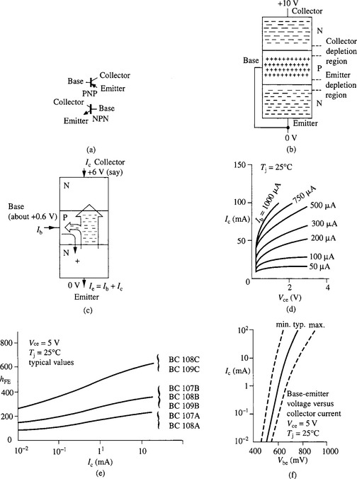
(b) NPN junction transistor, cut-off condition. Only majority carriers are shown. The emitter depletion region is very much narrower than the collector depletion region because of no reverse bias and higher doping levels. Only a very small collector leakage current Icb flows
(c) NPN small-signal silicon junction transistor, conducting. Only minority carriers are shown. The dc common emitter current gain is hFE = Ic/Ib, roughly constant and typically around 100. The ac small-signal current gain is hie = dIc/dIb = ic/ib
(d) Collector current versus collector/emitter voltage, for an NPN small-signal transistor (BC 107/8/9)
(e) hFE versus collector current for an NPN small-signal transistor
(f) Collector current versus base/emitter voltage for an NPN small-signal transistor
(Parts d to f reproduced by courtesy of Philips Electronics UK Ltd. www.semiconductors.philips.com)
Although the base/emitter junction behaves like a diode, exhibiting an incremental resistance of 25/Ie at the emitter, most of the emitter current appears in the collector circuit, as we have seen. The ratio Ic/Ib is denoted by the symbol hFE, the dc current gain or static forward current transfer ratio. As Figure 6.2d and e show, the value of hFE varies somewhat according to the collector current and voltage at which it is measured. When designing a transistor amplifying stage, it is necessary to ensure that any transistor of the type to be used, regardless of its current gain, Vbe, etc., will work reliably over a wide range of temperatures: the no-signal dc conditions must be well defined and stable. The dc current gain hFE is the appropriate parameter to use for this purpose. When working out the small signal stage gain, hfe is the appropriate parameter; this is the ac current gain dIc/dIb. Usefully, for many modern small signal transistors there is little difference in the value of hFE and hfe over a considerable range of current, as can be seen from Figures 6.2e and 6.3a (allowing for the linear vertical axis in the one and logarithmic in the other).
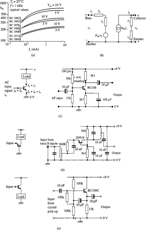
Figure 6.3 Small-signal amplifiers
(a)hfe versus collector current for an NPN small-signal transistor of same type as in Figure 6.2e.
(b) Common emitter equivalent circuit
(c) Common emitter audio amplifier, Ib = base bias or standing current; Ic = collector standing current; ic = useful signal current in load
(Reproduced by courtesy of Philips Electronics UK Ltd)
The performance of transistors can be described by a number of ways, some implying a particular model of the transistor’s internal circuit as in Figure 6.3b, while others simply relate conditions at the input port to those at the output. For use at the higher RF frequencies, certainly above 10 MHz say, the most useful approach is undoubtedly using ‘scattering parameters’ (or s-parameters). These are so called as they involve measuring the voltage reflected or scattered at input or output port in a matched system, for a given incident voltage. They are dealt with in detail in Appendix 2. However, of the many other sets of parameters used to describe transistor function, historically one of the most important is the hybrid parameter set. This uses a simple model not presupposing an internal circuit of the transistor (see Figure 6.4a and b). h11 is the input impedance and h21 the forward current transfer ratio, both measured with the collector short-circuited at ac, while h22 is the output admittance and h12 the voltage feedback ratio (dv1/dv2), both measured with the input open circuit to ac. This set of parameters is known as the hybrid parameters (or h-parameters) due to the mixture of units, impedance, admittance and pure ratios. A transistor can be used as an amplifier in three fundamentally different circuit configurations, but there is one feature common to all of these. Having only three leads, one of the electrodes of a transistor amplifier must be common to both the input circuit and the output circuit, as indicated by the dotted line in Figure 6.4b. Figure 6.3c shows a common emitter small-signal amplifier using the BC108, a transistor designed originally as a low-noise AF amplifier, but useful in not too demanding RF circuits up to several tens of megahertz. When employed in the common emitter circuit, h21 is known as hfe, which we have already met. Figure 6.4c shows hie, hre and hoe, the common emitter values of h11, h12 and h22 respectively, for the BC109. These parameters are for operation at the standing values of collector current and voltage indicated, at 1 kHz. At this low frequency, there is negligible phase shift through the transistor under the prescribed measurement conditions, so the parameters are all real, not complex. Using these parameters, the low-frequency performance of a common emitter stage such as in Figure 6.3c can in principle be calculated exactly. However, the h parameters will vary with collector current and voltage (the graphs give data for only two spot values of collector emitter voltage) and in any case, are only typical values. In fact, for all the parameter sets mentioned in the textbooks, only a few are quoted in manufacturers’ data, and maximum and minimum data are even scarcer. The advantage of s parameters is that they do not involve measurements made with a port terminated in open or short circuit, these being extremely difficult to implement precisely at RF. With s parameter measurements, the source and load impedance is 50 Ω, provided by the test ports of a network analyser.

(a)Generalized two-port black box. v and i are small-signal alternating quantities. At both ports, the current is shown as in phase with the voltage (at least at low frequencies), i.e. both ports are considered as resistances (impedances)
(b) Transistor model using hybrid parameters
(c) h-parameters of a typical small-signal transistor family (see also Figure 6.3a).
(Reproduced by courtesy of Philips Electronics UK Ltd. www.semiconductors.philips.com)
The common emitter configuration of Figure 6.3c offers potentially the highest gain of the three configurations (the actual gain will depend more on the circuit than the transistor) because there is current gain and, if the collector circuit load impedance is higher than the stage’s input impedance, there is voltage gain also. Figure 6.3d shows a common base stage used as an RF amplifier: the common base configuration is very suitable for this purpose because in a transistor such as the venerable 2N918 or its more modern counterparts, designed specially for use up to UHF, the collector emitter capacitance is very low, resulting in little internal feedback and thus a stable amplifier. However, the maximum gain available from a common base stage is less than for a common emitter stage (stability considerations apart), as the current gain of the device is slightly less than unity.
Figure 6.3e shows a common collector stage, often known as an emitter follower. Here, the voltage gain is nearly unity, but there is power gain, as the output impedance of the stage is much lower than its input impedance. It can thus drive a low load impedance without heavily loading the source.
In the early 1960s, the first practical junction field effect transistors made their appearance, though they had been described theoretically as early as 1952. Figure 6.5a shows the symbols for the device while Figure 6.5b and c show the construction and operation of the first type introduced, the depletion mode junction FET or JFET In this device, in contrast to the bipolar transistor, conduction is by means of majority carriers which flow through the channel between the source (analogous to an emitter) and the drain (analogous to a collector). The gate is a region of silicon of opposite polarity to the source-cum-substrate-cum-drain. When the gate is at the same potential as the source and drain, its depletion region is shallow and current carriers (electrons in the case of the N channel FET shown in Figure 6.5c) can flow between the source and the drain. The FET is thus a unipolar device; minority carriers play no part in its operation. As the gate is made progressively more negative, the depletion region extends across the channel depleting it of carriers, and eventually pinching off the channel entirely when Vgs reaches - VP, the pinch-off voltage. Thus for zero or small voltages of either polarity between source and drain, the device can be used as a passive voltage controlled resistor. The JFET is however more normally employed in the active mode as an amplifier (Figure 6.5d) with a positive supply rail (for an N channel FET), much like an NPN transistor stage. Note that even with zero gate/source reverse bias, as the drain becomes more and more positive, the gate becomes negative relative to it, so that the channel becomes pinched off at the drain end. This is clearly shown in Figure 6.5c and e, and as a result, further increase in drain voltage does not increase the drain current appreciably. So as Figure 6.5e shows, the typical drain characteristic is pentode-like. Provided that the gate is reverse biased, as it normally will be, it draws no current, making the FET a close cousin of the pentode at dc and low frequencies. At RF it behaves more like a triode, owing to the drain gate capacitance Cgd, analogous to the collector base capacitance of a bipolar transistor. The positive excursions of gate voltage of an N channel FET (or the negative excursions in the case of a P channel device) must be limited to less than 0.5 V to avoid turn-on of the gate/source junction, otherwise the benefit of a high input impedance is lost.
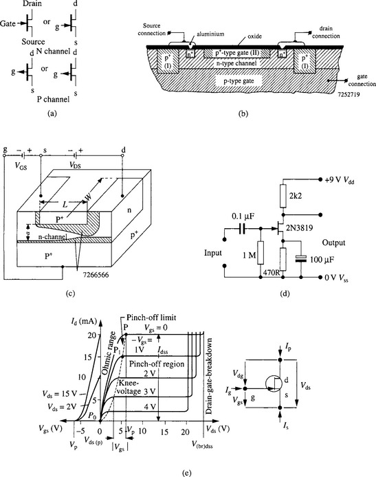
Figure 6.5 Depletion mode junction field effect transistors
(b) Structure of an N channel JFET
(c) Sectional view of an N channel JFET. The P+ upper and lower gate regions should be imagined to be connected in front of the plane of the paper, so that the N channel is surrounded by an annular gate region. The cross-hatched area indicates the pinch-off region
(d) JFET audio-frequency amplifier
(f) Characteristics of N channel JFET; pinch-off voltage Vp = − 6 V
(Parts b, c and e reproduced by courtesy of Philips Electronics UK Ltd. www.semiconductors.philips.com)
In the metal oxide field effect transistor or MOSFET (Figure 6.6a) the gate is insulated from the channel by a thin layer of silicon dioxide, which is an insulator: thus the gate circuit never conducts. The channel is a thin layer formed between the substrate and the oxide. In the enhancement (normally off) MOSFET, a channel of semiconductor of the same polarity as the source and drain is induced in the substrate by the voltage applied to the gate (Figure 6.6b). In the depletion (normally on) MOSFET, a gate voltage is effectively built in by ions trapped in the gate oxide (Figure 6.6c). Figure 6.6a shows symbols for the four possible types and Figure 6.6d summarizes the characteristics of the N channel types. Since it is much easier to arrange for positive ions to be trapped in the gate oxide than negative ions or electrons, P channel depletion MOSFETs are not generally available. Indeed, for JFETs and MOSFETs of all types, N channel far outnumber P channel devices. RF power MOSFETs are invariably N type.

Figure 6.6 Metal-oxide semiconductor field effect transistors
(a)MOSFET types. Substrate terminal b (bulk) is generally connected to the source, often internally
(b) Cross-section through an N channel enhancement (normally off) MOSFET
(c) Cross-section through an N channel depletion (normally on) MOSFET
(d) Examples of FET characteristics: (i) normally off (enhancement); (ii) normally on (depletion and enhancement); (iii) pure depletion (JFETs only)
(Reproduced by courtesy of Philips Electronics UK Ltd. www.semiconductors.philips.com)
Note that whilst the source and substrate are internally connected in most MOSFETs, in some - such as the Motorola 2N351 - the substrate connection is brought out on a separate lead. In these cases it is possible to use the substrate as another input terminal. For example, in a frequency changer, the signal could be applied to the gate and the local oscillator (LO) to the substrate, resulting in reduced LO radiation; in an IF amplifier, the signal could be connected to the gate and the automatic gain control voltage (AGC) to the substrate. In high power RF MOSFETs, the substrate is always internally connected to the source.
In the N channel dual-gate MOSFET (Figure 6.7) there is a second gate between gate 1 and the drain. Gate 2 is typically operated at + 4 V with respect to the source and serves the same purpose as the screen grid in a tetrode or pentode. It results in a reverse transferor feedback-capacitance Crss between drain and gate 1 of only about 0.01 pF, against 1 pF or thereabouts for small-signal JFETs, single-gate MOSFETs and bipolar transistors designed for RF applications. As Figure 6.7c shows, the dual-gate MOSFET is equivalent to a two-transistor amplifier stage consisting of a common source FET driving a common gate FET. It is thus an example of an amplifier known as the cascode stage, which is described in more detail in Chapter 7.
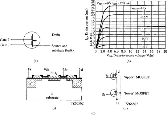
(a)Dual-gate N channel MOSFET symbol. Gate protection diodes, not shown, are fabricated on the chip in many device types. These limit the gate/source voltage excursion in either polarity, to protect the thin gate oxide layer from excessive voltages, e.g. static charges
(b) Drain characteristics (3N203/MPF203).
(c) Construction and discrete equivalent of a dual-gate N channel MOSFET.
(Reproduced by courtesy of Philips Electronics UK Ltd. www.semiconductors.philips.com) (Copyright of Freescale Semiconductor, Inc. 2006, Used by permission)
Linearity is an important consideration in amplifiers and other devices for RF applications. This is because a lack of linearity (distortion) can result, in a receiver, in the degradation of a wanted small signal in the presence of large unwanted ones and, in the case of a transmitter, in the unintentional transmission of energy at frequencies other than the authorized transmit frequency, interfering with other users. In an ideal amplifier, the waveform of the output is identical to that of the input - only larger. Thus the transfer characteristic of the stage is perfectly linear. There are two main ways in which the characteristic may depart from the ideal. Firstly, the gain may differ on positive- and negative-going half-cycles of the input; Figure 6.8a(i) to (iii) shows how this results in a spurious component in the output at twice the input frequency. This is called second order distortion, since there is an output component proportional to the square of the input voltage. The other common form of distortion is called third order distortion, producing a spurious component in the output at three times the frequency of the input signal. This is illustrated in Figure 6.8b and c, showing what happens when compression of the signal occurs at both positive and negative peaks, due to a cubic or S-shaped component in the transfer characteristic. The top waveform in Figure 6.8c is the amount by which the output falls short of what it would have been had the transfer characteristic been linear. This shortfall consists of two components, one at ωt representing gain compression, and one at the third harmonic 3ωt.

When two signals are present simultaneously, as will commonly happen in the front end of a radio receiver, second-order distortion will also result in products at frequencies equal to the sum and difference of the two input signals. One of these spurious products may fall on top of a small wanted signal, preventing its reception entirely. With third-order distortion, signals at f1 and f2 will result in spurious products at 2f1 - f2 and 2f2 - f1, again possibly jamming a small wanted signal. This is illustrated in Figure 6.8d. Third-order distortion is particularly undesirable, since the spurious products fall close to f1 and f2. If f1, f2 and the wanted signal are all close together, it will be impossible to provide sufficient selectivity to reduce the amplitude of f1 and/or f2 to a level where their third-order intermodulation products are negligible. High linearity is a desirable feature of an active device such as an amplifier, but careful circuit and equipment design is needed if the linearity is to be realized in practice. At the circuit level, linearity is improved by accepting a modest stage gain and possibly including an additional stage, rather than seeking to obtain the maximum possible gain from every stage. Careful attention to layout and screening to avoid feedback (resulting in near instability) is also essential. However carefully designed, there must come a point as the input signal level is increased, where an amplifier overloads. Figure 6.9a shows the input-output relation for an amplifier with a gain of G dB. At low levels, the output rises decibel for decibel with the input, but for very large inputs the amplifier is driven into limiting and reaches its ‘saturated output power’. In saturation, there will be a substantial level of harmonic power in the output of the amplifier in addition to the wanted fundamental output, at least in the case of an amplifier stage which does not incorporate a tuned tank circuit. The level at which the fundamental output is 1 dB less than it would be in the absence of limiting is called the compression point.
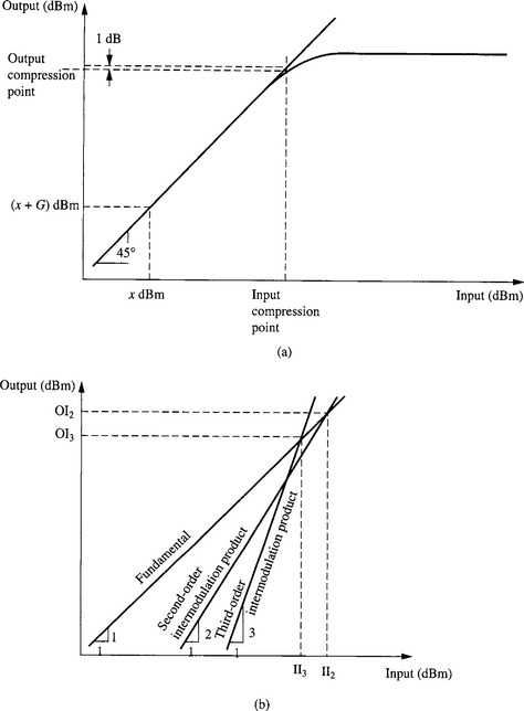
Figure 6.9b shows that when two fundamentals are applied to an amplifier simultaneously, for low input levels the second-order and third-order intermodulation products are way below the wanted output. Nevertheless, theoretically for every decibel by which the input signals rise, the second-order intermodulation products rise by 2 dB and the third-order products by 3 dB. Empirically, this rule of thumb is found to hold for well-behaved circuits, up to about 10 dB below the compression point. If the results are plotted as in Figure 6.9b and extrapolated, eventually the level of the intermodulation products will notionally intersect the level of the fundamental. The corresponding second- and third-order input intercept points II are shown on the x axis and the output intercept points OI on the y axis. A cheap way for the sharp manufacturer to make his amplifier sound good is to talk a lot about the input intercept points and then just barely mention in passing that the figures he quotes are for the output intercept points.
Mixers are used to translate a signal from one frequency fa to another, fb, by means of a local oscillator frequency fLO. fb may be either fa + fLO or fa - fLO. Both active and passive mixers are used and both types will be considered here. A mixer is subject to stringent, not to say contradictory constraints. It is required to exhibit a strong second order characteristic to signals applied to the signal and LO ports, to produce the required sum and difference frequencies, but to be exceedingly linear to two or more large unwanted signals applied to the signal port, in order not to produce second order and more importantly third order intermodulation products. It is also convenient if the mixer is balanced, that is to say that the LO input does not appear at the output port, or alternatively that the signal input does not so appear. A professional communications receiver will usually use a double-balanced mixer (DBM), i.e. one where neither the signal nor the LO input appear at the output, whilst the LO does not appear at the RF input port either.
Figure 6.10a shows on the left the circuit diagram of a typical passive DBM (also known as a ring mixer since all four diodes are connected sequentially anode to cathode), using a matched quad of Schottky diodes. On the right is shown the effective circuit on one half-cycle of the LO drive, when two of the diodes are conducting heavily and the other two cut off. The result is to connect the signal at the R (RF) input to X (IF) port in one phase, and then in the reverse phase on the next half cycle of the LO waveform. The signal is effectively multiplied by +1 and −1 on alternate LO half-cycles. The fundamental of the LO and the signal therefore mix to produce sum and difference components at the X port. In practice, the suppression of the signal and LO inputs at the X port in a passive DBM is limited, typically 40-50 dB midband and more like 15-25dB at the edges of the device’s designed operating frequency range. The conversion loss to the signal input is typically 6.5 dB. Of this, 3 dB is inherently due to the split of the output power between the sum and difference frequencies; the rest is due to resistive losses in the diodes and transformers. If the input at the R port includes large unwanted signals there may be other unwanted outputs at IF in addition to those due to intermodulation products. These are all varieties of ‘spurious response’ due to imperfections in the DBM which the mixer manufacturer tries to minimize: they are discussed further in later chapters. However, the level of spurious responses exhibited by a mixer in practice depends as much if not more upon the user than upon the manufacturer. The spurious responses are minimized when the mixer is run with interfaces having a very low VSWR at all frequencies, at all of its three ports. The manufacturer’s published performance data is measured with test gear having a 50 Ω characteristic impedance, usually with a 10-dB 50-Ω pad at each port for good measure. This is quite unrepresentative of actual conditions of use, but it would be impossible to tabulate the performance at all frequencies for all possible combinations of VSWR at the mixer’s three ports. In practice, the mixer’s R port is likely to be driven from a low-noise amplifier with a poor output VSWR, or worse still from a band-pass filter, whilst the IF X port is likely to be terminated in a band-pass roofing filter. Pads at the R and X ports are clearly undesirable as they will worsen the receiver’s noise figure. A pad at the L port can be useful, albeit at the expense of an increased LO power requirement. A filter connected directly to a mixer port may provide a reasonable match in its pass band, but will reflect energy back into the mixer in its stop band, where its VSWR is very large. Means of avoiding this dilemma are discussed in Chapter 15.

Figure 6.10 Double-balanced mixers (DBMs)
(a)The ring modulator. The frequency range at the R and L ports is limited by the transformers, as also is the upper frequency at the X port. However, the low-frequency response of the X port extends down to 0 Hz (dc)
(b) Basic seven-transistor tree active double-balanced mixer. Emitter-to-emitter resistance R, in conjunction with the load impedances at the outputs, sets the conversion gain
(c) The transistor tree circuit can be used as a demodulator (see text). It can also, as here, be used as a modulator, producing a double-sideband suppressed carrier output if the carrier is nulled, or AM if the null control is offset. The MC1496 includes twin constant current tails for the linear stage, so that the gain setting resistor does not need to be split as in b.
(d) High dynamic range DBM (see text) band, where its VSWR is very large. Means of avoiding this dilemma are discussed in Chapter 15.
(Copyright of Freescale Semiconductor, Inc. 2006, Used by permission)
Another well-known scheme, not illustrated here, uses MOSFETs as switches instead of diodes [1]. It is thus, like the Schottky diode ring DBM, a passive mixer, since the MOSFETs are used solely as voltage-controlled switches and not as amplifiers. Reference 2 describes a single balanced active MOSFET mixer providing 16dB conversion gain and an output third-order intercept point of +45dBm. Figure 6.10b shows an active DBM of the seven-transistor tree variety; the interconnection arrangement of the four upper transistors is often referred to as a Gilbert cell. The emitter-to-emitter resistance R sets the conversion gain of the stage; the lower its value, the higher the conversion gain but the worse the linearity, i.e. the lower the third-order intercept point. This circuit is available in IC form (see Figure 6.10c) from a number of manufacturers under the type numbers 1496 or 1596, whilst derivatives with a higher dynamic range have been produced [3]. Figure 6.10d shows one of the ways the signal handling capability and linearity of the passive DBM can be increased, usually at the expense of a requirement for increased LO drive power. The resistors in series with the diodes swamp and thus stabilize the on resistance of the diodes, whilst the increased forward volt drop increases the reverse bias on the off diodes, minimizing (variations in) their reverse capacitance. High performance DBMs may accept LO drive powers up to + 27 dBm.
The term ‘active components’ for RF must include, in addition to IC mixers, a host of ICs designed to operate as RF or IF amplifier stages, or as complete IF strips, often complete with local oscillator, mixer, and in some cases an RF stage as well. However, the operation of these is so closely bound up with the application circuits, that they are covered in Chapter 7.
References
1. Rafuse, R.P. Symmetric MOSFET mixers of high dynamic range. International Solid State Conference Session XI. University of Pennsylvania: 1968:122–123.
2. Oxner, E.S. Single balanced active mixer using MOSFETs. Power FETs and Their Applications. Prentice Hall: Englewood Cliffs N.J. 07632, 1982:292.