
RF transmission lines
Transmission line operation at d.c.
In the later part of this chapter, how a transmission line behaves when conducting radio frequency signals will be discussed. But a useful insight into what happens when such a signal arrives at the end of a transmission line, and how it gets reflected, can be gained by considering a signal of frequency 0 Hz, i.e. the d.c. case. This also turns out to be an important consideration in some radio frequency equipments, namely radar transmitters, as will appear later. For simplicity, let’s assume the transmission line is in air, or even in vacuo, so that the velocity of propagation is nearly the speed of light, 300 mm per nanosecond1, that it has a ‘characteristic impedance’ of 300O and that the line is open circuit at the far end. Consider the line before the battery is connected between the two copper conductors (Figure 3.1).
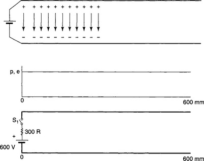
At every point along the line there are equal numbers of protons, fixed, and electrons, mostly fixed, per unit length. But there are also some ‘free electrons’, one per copper atom, forming a sort of ‘conducting gas’ within the two conductors. This has been plotted in a graph at the top of Figure 3.1, where the x axis represents 600 mm, the length the line. Before the switch is closed, the equal number of protons and electrons per unit length is indicated by the line labelled ‘p, e’. Thus there is no net charge at any point on either conductor, and the potential difference between them is everywhere zero.
An atom is not proprietorial about its free electron: if the latter departs to the left as part of an electric current, the positive charge on the nucleus is happy to let it go, provided that another electron comes along from the right to take its place, which will always be the case in a complete circuit.
Now consider the case when the switch is closed, Figure 3.2. Conventional current flows into the top conductor of the line, but in fact a conventional current flowing to the right actually consists purely of electrons moving to the left (at least, in a metallic conductor, which− unlike a semiconductor− has no mobile positive charges or ‘holes’).

Assuming the velocity of the wavefront on the line is the same as the speed of light (for an open air-line, it won’t be that much less), then after half a nanosecond it will have reached the point indicated by the line AA’, and after a further half nanosecond it will have reached BB’, as indicated in Figure 3.2. The instant the switch is closed, the leftmost electron in the upper conductor (the ‘first’ electron) will start to move, eventually passing via the switch and into the matched source, the internal resistance and emf of which have been shown separately. The second electron now finds the third electron closer to it than the first. As like charges repel each other the more, the closer they are together, the second electron experiences a net force pushing it to the left and starts to move leftwards also. Now, the third electron finds the fourth electron closer to it than the second and also starts to move and so on. The electrons may be moving at a snail’s pace relative to the speed of light, but the disturbance just described propagates along the line at the speed of light, reaching BB’ in just a nanosecond.
To the right of BB’ there are still equal numbers of protons and electrons per unit length of line, so there is no net charge and the voltage on the line there is as yet zero. To the left of BB’ a line of electrons is moving to the left at a constant speed, the spacing between the moving electrons being everywhere equal, x+ δ say; slightly greater than to the right of BB’. Therefore, there is everywhere a slight deficit of electrons per unit length of the upper conductor, their number being represented by the dashed line ‘e’ in Figure 3.2 (not to scale). The resultant constant net positive charge per unit length is responsible for the constant positive potential on the line, relative to the lower conductor, indicated in Figure 3.2 by the solid bold line labelled ’V. With a line of electrons all moving at the same speed and with a constant spacing between them, the current in the line to the left of BB’is shown as a dotted line. The ratio of V to I gives the ‘characteristic impedance’ or ‘surge impedance’ of the line, which has been assumed to be 300 Ω, a typical value for a two-wire air-line, though it could be anywhere from about a third to five times that value, depending upon the thickness of the conductors, their spacing and the dielectric separating them.
Exactly the same mechanism which has been used to account for the appearance of a positive charge on the upper conductor, accounts equally well for the appearance of a negative charge on the lower conductor. Only now, as conventional current flows from the source into the upper conductor, it returns from the lower conductor, into the negative pole of the source. This implies that the negative pole forces electrons into the left-hand end of the lower line. What was the first electron there now finds one closer to it on its left than the second electron on its right and so on, so to the left of BB’ the electrons are slightly closer together (x− δ) than to the right, all equally spaced and moving rightwards at a constant speed. They thus constitute a conventional negative current flow to the left, indicated by the dotted line below the baseline in the lower graph in Figure 3.2.
Although events on the upper and lower conductors have been described separately, the boundary between the charged and uncharged sections of the line proceeds at the same rate on both conductors, and indeed this common boundary is the wavefront. Also, the foregoing might seem to imply a neat single line of free electrons, rather like peas in a peashooter. But the current of 1A flowing in the line consists of the passage past any point of a charge of one Coulomb(1C) per second. The charge on an electron is 1.602 × 10⁻¹⁹C, so there are 6.242 × 10¹⁸ electrons entering the lower and leaving the upper conductor per second. The speed with which the electrons are moving depends of how many of them are involved in carrying the current. In a line composed of very thin conductors, the current will presumably be carried by fewer electrons, travelling faster, than in one with very thick conductors. In either case, the velocity of the electrons is very much less than that of light. Assuming the same conductor spacing, these two lines would clearly have very different characteristic impedances, so the applied voltage needed to cause a current of 1A to flow would differ greatly. Nevertheless, the mechanism of propagation of the wavefront on the line is as described; but many electrons are involved rather than just the ‘first’, ‘second’, etc. One must assume that the deficit of electrons in the upper conductor (the positive charge, due to nuclei short of one attendant electron) distributes itself on the surface, around the circumference, in a mirror image of the distribution of the additional electrons on the lower conductor, there being no deficit of electrons within the upper conductor.
During the 2 ns the wavefront takes to traverse the 600 mm of line depicted in Figure 3.2, the source supplies 600 nJ/ns of energy to the line− delivered by a current of 1A− and ‘thinks’ it is connected to a 300Ωresistor. If the length of the line is infinite, the source will continue to ‘see’ a 300Ω resistor indefinitely, and similarly if the end of the line in Figure 3.1 is terminated in a real 300Ω resistor. But the 300W dissipation in the resistor would not commence until 2 ns after the switch is closed. During that time, 600 nJ of energy is stored in the electric and magnetic fields of the line, and 300 W would continue to be dissipated in the resistor for 2 ns after the switch were subsequently opened.
Now consider in detail what happens at 2 ns, when the wavefront reaches the open circuit end of the line in Figure 3.2. The conventional ‘explanation’ is that an open circuit reflects the voltage in-phase and the current out of phase, while a short circuit reflects the voltage out of phase and the current in-phase. A more complete analysis follows. At time t = 2 ns the source has delivered 600 nJ of energy to the line (up to this instant the termination, if any, is immaterial).
So the source has supplied 2 nC of charge to the line.
There is a uniform PD of 300 V along the line.
Q = CV, therefore 2 nC = C × 300 where C is the capacitance between the conductors. (It’s just unfortunate that C stands both for capacitance and Coulomb.)
Capacitance of line = 2 =![]() = 6.667 × 10⁻¹² Farads.
= 6.667 × 10⁻¹² Farads.
Energy stored =![]() CV2 =
CV2 =![]() ×6.667×10−12 × 3002 = 300 nJ.
×6.667×10−12 × 3002 = 300 nJ.
This is half the energy put in, so the rest must be in the magnetic field.
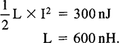
It may seem strange to talk of the inductance of a 600 mm line which is open circuit, but it is quite logical if attention is restricted purely to the instant t = 2 ns, when there is current flowing in the whole length of each conductor.
Line impedance = (L/C)05 = (600 × 10−9/6.667 × 10−12)05= 300Ω, which all seems to tie up. Half of the total energy supplied is stored in the electric field, and half in the magnetic.
In the open circuit case, after t = 2 ns, what actually happens is the following: The electron at the extreme right-hand end of the lower conductor (the ‘last’ electron) cannot move substantially to the right; it is at an open circuit. But the potential between the conductors at the input is still 300 V, so the source continues to feed electrons into the left-hand end of the line− since it still ‘sees’ a 300 O load. The ‘train’ of electrons thus continues on its route, forcing the ‘second but last’ electron, closer to the stationary last electron. When the spacing between them falls from (x−) to (x− 2δ), the force of repulsion between them becomes so great as to force the second but last electron to a halt. Successively, the third but last and other electrons also grind to a halt, so the current at the right-hand end of the line is zero. The boundary between the moving and stationary electrons propagates to the left at the speed of light, even though the speed of movement of individual electrons is comparatively very slow.
Simultaneously, when the right-most electron in the upper conductor starts to move to the left, becoming the last in a train of electrons streaming to the left, the nucleus of the right-most atom finds no electron arriving from the right to replace it. It is therefore unwilling to relinquish its electron entirely. The electron is therefore promptly uncoupled again from the train. The next atom in from the left is similarly unwilling to relinquish its electron, since no replacement is available from the right. The second from right electron is thus also uncoupled from the train, but the spacing between these two now stationary electrons is (x+ 2d). The train continues to the left, surrendering 1 nC/ns of charge to the source, but getting steadily shorter as more and more electron ‘trucks’ are abandoned on the rails, all at a spacing of (x+ 2δ), until after 3 ns, the situation is as depicted in Figure 3.3.

Whereas electron spacing of (x ± δ) on the conductors equated to a potential difference between them of 300 V, (x ± 2δ) equates to a potential difference 600 V.
To the right of BB’, the deficit of electrons per unit length of the upper conductor is twice as great as to the left of BB’, indicated by the dashed line labelled ‘e’ on the graph. Therefore the potential on the upper conductor, relative to the lower, is now 600 V, as per the solid black line labelled V, while the current on the line to the right of BB’ is zero, since the electrons there are stationary. At 4 ns after switch S1 was closed, the length of the train has reduced to zero, all the electrons having been abandoned at a spacing of (x+ 2δ), the electrons on the lower line are all at (x− 2δ) and the potential on the line is everywhere 600 V. There is thus no potential difference between the two ends of the 300Ω source resistor, so the flow of conventional current being supplied by the source EMF ceases abruptly, leaving as many extra electrons per unit length on the lower conductor as the deficit of electrons per unit length on the upper conductor.
During the period t = 2 ns to t = 4 ns, the length of line in which current is flowing reduces steadily from 600 mm to zero, and the inductance reduces similarly from 600 nH to zero, converting the 300 nJ of energy stored in the magnetic field to more energy stored in the electric field. Together with the 600 nJ supplied by the source during this period, this brings the total energy stored in the line to 1200 nJ, all stored in the electric field.
The apparent flow of conventional current from the upper to the lower conductor is what is meant by displacement current, a concept introduced by Maxwell to retain consistency with Kirchoff’s First Law, in cases where there is no obvious circuit, such as when charging a capacitor. Note that the notional displacement current only flows where the electric field strength (voltage gradient) is changing. In Figure 3.2, at 1 ns after the switch S1 is closed, the voltage on the line to the left of BB’ is everywhere constant at 300 V, and to the right of BB’ is everywhere zero. So the displacement current of 1A flows only at the point where the wavefront is. This implies that if the voltage step is instantaneous, the length of conductors between which the displacement current flows is infinitesimal, and the displacement current density therefore infinite. This is a major difficulty, and one reason why the concept of displacement current can be consigned to history.
Is there a crucial difference between the 300Ω characteristic impedance of the line, and a capacitor, or a 300Ω resistor? At twice the voltage, a capacitor stores four times as much energy, and a resistor dissipates energy at four times the rate. In the case of the open circuit line, at 2 ns, the energy stored at 300 V is 600 nJ, and after 4 ns, at twice the voltage, the stored energy only doubles to 1200 nJ. But after 2 ns, only 300 nJ is stored in the capacitance of the line, the other half of the energy supplied being stored in its inductance. Thus the energy stored in the line’s capacitance quadruples when the voltage doubles to 600 V. During the 4 ns, 1200 nJ has been dissipated in the internal resistance of the source, so the total energy supplied by the 600 V ideal generator is 2400 nJ.
At 4 ns, the energy stored in the line is 1/2CV2 = 1/2 × 6.667 × 10−12 × 6002 = 1200 nJ, exactly the same as for a discrete capacitor of the same capacitance as the line. The crucial difference is that if the discrete capacitor is connected to a 300Ω resistor, it will deliver an initial 2 A, decaying exponentially whereas the charged line will deliver a constant 1A for 4 ns, ceasing abruptly thereafter. This is why a delay line rather than a capacitor is used to supply anode power to a magnetron, to form a pulse flat-top pulse in a radar transmitter.
A similar analysis will show that in the case of a line short circuited at its far end, the incident wave is reflected out of phase or inverted, there can after all never be a voltage across a short circuit. The current is reflected in-phase, so that after 4 ns − in the case of a 600 mm line − a short circuit appears at the input to the line and the current supplied by the generator doubles to 2 A.
Transmission line operation at r.f.
RF transmission lines are used to convey a radio frequency signal with minimum attenuation and distortion. They are of two main types, balanced and unbalanced. A typical example of the former is the flat twin antenna feeder with a characteristic impedance of 300Ω often used for VHF broadcast receivers, and of the latter is the low loss 75Ω coaxial downlead commonly used between a UHF TV set and its antenna.
Characteristic impedance can be explained in conjunction with Figure 3.4 as follows. Leaving aside the theoretical ideal voltage source, any practical generator (source of electrical power, e.g. a battery) has an associated internal resistance, and the maximum power that can be obtained from it flows in a load whose resistance equals the internal resistance. In the case of a source of RF energy, for example a signal generator, it is convenient if the source impedance is purely resistive, i.e. non-reactive, as then the power delivered to a resistive load (no power can ever be delivered to a purely reactive load) will be independent of frequency.
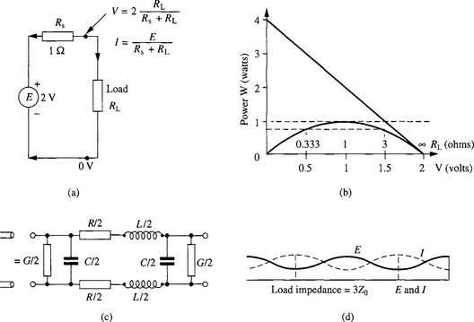
Figure 3.4 Matching and transmission lines
(a) Source connected to a load RL
(b) E = 2V, Rs = 1Ω. Maximum power in the load occurs when RL = Rs and V = E/2 (the matched condition, but only falls by 25% for RL = 3Rs and RL = Rs/3. For the matched case the total power supplied by the battery is twice the power supplied to the load. On short-circuit, four times the matched load power is supplied, all dissipated internally in the battery
(c) Two-wire line: balanced equivalent of short section
(d) Resultant voltage and current standby waves when load resistance = 3Z0
In Figure 3.4a and b, a source resistance of 1Ω and a maximum available power of 1 W is shown, for simplicity of illustration. However, the usual source resistance for a signal generator is 50Ω unbalanced, that is to say the output voltage appears on the inner lead of a coaxial connector whose outer is earthy (carries no potential with respect to ground). Imagine such an output connected to an infinitely-long loss-free coaxial cable. If the diameters of the inner and outer conductors are correctly proportioned (taking into account the permittivity of the dielectric), the signal generator will deliver the maximum energy possible to the cable; the cable will appear to the source as a 50Ω load and the situation is the same as if a 50 O resistor terminated a finite length of the cable.
Figure 3.4c shows a short length of a balanced feeder, showing the series resistance and inductance of the conductors and the parallel capacitance and conductance between them, per unit length (the conductance is usually negligible). Denoting the series and parallel impedances as ![]() and
and ![]() respectively, the characteristic impedance
respectively, the characteristic impedance ![]() of the line is given by
of the line is given by ![]() . If G is negligible and jωL
. If G is negligible and jωL ![]() R, then practically
R, then practically ![]() and the phase shift β along the line is
and the phase shift β along the line is ![]() radians per unit length. Thus the wavelength of the signal in the line (always less than the wavelength in free space) is given by
radians per unit length. Thus the wavelength of the signal in the line (always less than the wavelength in free space) is given by ![]()
Although at RF, jωL ![]() R, the resistance is still responsible for some losses, so that the signal is attenuated to some extent in its passage along the line. The attenuation per unit length is given by the full expression for the propagation constant
R, the resistance is still responsible for some losses, so that the signal is attenuated to some extent in its passage along the line. The attenuation per unit length is given by the full expression for the propagation constant ![]() where a is the attenuation constant per unit length, in nepers. Nepers express a power ratio in terms of natural logs, i.e. to base e rather than to base 10: 1 neper = 8.7 dB. In practice, R will be greater than the dc resistance, due to the skin effect, which increases with frequency; the attenuation ‘constant’ is therefore not really a constant, but increases with increasing frequency.
where a is the attenuation constant per unit length, in nepers. Nepers express a power ratio in terms of natural logs, i.e. to base e rather than to base 10: 1 neper = 8.7 dB. In practice, R will be greater than the dc resistance, due to the skin effect, which increases with frequency; the attenuation ‘constant’ is therefore not really a constant, but increases with increasing frequency.
If a 50Ω source feeds a lossless 50Ω coaxial cable but the load at the far end of the cable is higher or lower than 50Ω then the voltage appearing across the load will be higher or lower and the current through it lower or higher respectively than for a matched 50Ω load. Some of the voltage incident upon the load is reflected back towards the source as explained earlier, either in phase or in antiphase, and this reflected wave travels back towards the source with the same velocity as the incident wave: this is illustrated in Figure 3.4d for the case of a 150Ω load connected via a 50Ω cable to a 50Ω source, i.e. a load of 3 × Z0. The magnitude of the reflected current relative to the incident current is called the reflection coefficient, ρ, and is given by
In Figure 3.4d, since ZL = 3Z0, ρ=−0.5, the minus sign indicating that the reflected current is reversed in phase. Thus if the incident voltage and current is unity, the net current in the load is the sum of the incident and reflected currents, = 1− 0.5 = 0.5 A. The net voltage across the load is increased (or decreased) in the same proportion as the current is decreased (or increased), so the net voltage across the load is 150% and varies along the line between this value and 50% of the incident voltage. The ratio of the maximum to minimum voltage along the line is called the ‘voltage standing wave ratio’, VSWR, and is given by VSWR = (1− ρ)/(1+ ρ) (or its reciprocal, whichever is greater than unity), so for the case in Figure 3.4d where ρ =−0.5, the VSWR = 3. In a line terminated in a resistive load equal to the characteristic impedance Z0 (a matched line), ρ = 0 and the VSWR equals unity. Note that the characteristic impedance of a coaxial cable may show minor variations along its length, either as a result of its manufacture, or due to stress such as a tight band when installed. For further details see Appendix 5.
If a length of 50Ω line is exactly λ/2 or a whole number multiple thereof, the source in Figure 3.4d will see a 150Ω load, but if it is λ/4, 3λ/4, etc., it will see a load of 16.7Ω. In fact, a quarter-wavelength of line acts as a transformer, transforming a resistance R1 into a resistance ![]() . The same goes for reactances X1 and X2 (but note that if X1 is capacitive X2 will be inductive and vice versa) and for complex impedances Z1 and Z2. Thus a quarter-wavelength of line of characteristic impedance
. The same goes for reactances X1 and X2 (but note that if X1 is capacitive X2 will be inductive and vice versa) and for complex impedances Z1 and Z2. Thus a quarter-wavelength of line of characteristic impedance ![]() can match a load R2 to a source R1 at one spot frequency, and over about a 10% bandwidth in practice. Note that the electrical length of a line depends upon the frequency in question. If a line is exactly λ/4 long at one frequency, it will appear shorter than λ/4 at lower frequencies and longer at higher, so a quarter-wave transformer is inherently a narrow band device.
can match a load R2 to a source R1 at one spot frequency, and over about a 10% bandwidth in practice. Note that the electrical length of a line depends upon the frequency in question. If a line is exactly λ/4 long at one frequency, it will appear shorter than λ/4 at lower frequencies and longer at higher, so a quarter-wave transformer is inherently a narrow band device.
A quarter-wave transformer will transform a short circuit into an open circuit and vice versa, and a line less than λ/4 will transform either into a pure reactance. This is illustrated in Figure 3.5a. Power (implying current in phase with the voltage) is shown flowing along a loss-free RF cable towards an open circuit. (Figure 3.5a is a snapshot at a single moment in time; the vectors further along the line appear lagging since they will not reach the same phase as the input vectors until a little later on.) On arriving, no power can be dissipated as there is no resistance; the conditions must in fact be exactly the same as would apply at the output of the generator in Figure 3.4a if it were unterminated, i.e. an open-circuit terminal voltage of twice the voltage which would exist across a matched load, and no current flowing. The only way this condition can be met is if there is a reflected wave at the open-circuit end of the feeder, with its voltage in phase with the incident voltage and its current in antiphase with the incident current. This wave propagates back towards the source and Figure 3.5a also shows the resultant voltage and current. It can be seen that at a distance of λ/8 from the open circuit, the voltage is lagging the current by 90°, as in a capacitor. Moreover, the ratio of voltage to current is the same as for the incident wave, so the reactance of the apparent capacitance in ohms equals the characteristic impedance of the line. The reactance is less than this approaching λ/4 and greater approaching the open end of the line. Similarly, for a line less than λ/4 long, a short-circuit termination looks inductive.
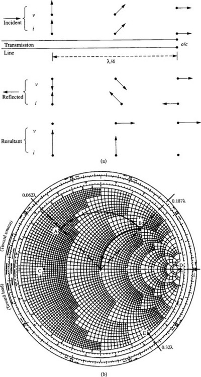
The way impedance varies with line length for any type of termination is neatly represented by the Smith chart (Figure 3.5b). The centre of the chart represents Z0, and this is conventionally shown as a ‘normalized’ value of unity. To get to practical values, simply multiply all results by Z0, e.g. by 50 for a 50Ω system. The chart can be used equally well to represent impedances or admittances. The horizontal diameter represents all values of pure resistance or conductance, from zero at the left side to infinity at the right. Circles tangential to the right-hand side represent impedances with a constant series resistive component (or admittances with a constant shunt conductance component). Arcs branching leftwards from the right-hand side are loci of impedances (admittances) of constant reactance (susceptance), in the upper half of the chart representing inductive reactance or capacitive susceptance. Circles concentric with the centre of the chart are loci of constant VSWR, the centre of the chart representing unity VSWR and the edge of the chart a VSWR of infinity. Distance along the line from the load back towards the source can conveniently be shown clockwise around the periphery, one complete circuit of the chart equalling half a wavelength. The angle of the reflection coefficient, which is in general complex (only being a positive or negative real number for resistive loads) can also be shown around the edge of the chart.
The Smith chart can be used to design spot frequency matching arrangements for any given load, using lengths of transmission line. (It can also be used to design matching networks using lumped capacitance and inductance; see Appendix 1.) Thus in Figure 3.5b, using the chart to represent normalized admittances, the point A represents a conductance of 0.2 in parallel with a (capacitive) susceptance of+j0.4. Moving a distance of (0.187− 0.062)λ = 0.125λ towards the source brings us to point B where the admittance is conductance 1.0 in parallel with +j2.0 susceptance. (Continuing around the chart on a constant VSWR circle to point C tells us that without matching, the VSWR on the line would be 1/0.175 = 5.7.) Just as series impedances add directly, so do shunt admittances. So if we add a susceptance of −j2.0 across the line at a point 0.125λ from the load, it will cancel out the susceptance of +j2.0 at point B. In fact, the inductive shunt susceptance of −j2.0 parallel resonates with the +j2.0 capacitive susceptance, so that viewed from the generator, point B is moved round the constant conductance line to point F, representing a perfect match. The −j2.0 shunt susceptance can be a ‘stub’, a short-circuit length of transmission line. Point E represents −j2.0 susceptance and the required length of line starting from the short circuit at D is (0.32−0.25)λ = 0.07λ. This example of matching using lengths of transmission lines ignores the effect of any losses in the lines. This is permissible in practice as the lengths involved are so small, but where longer runs (possibly many wavelengths) of coaxial feeder are involved, e.g. to or from an antenna, the attenuation may well be significant. It will be necessary to select a feeder with a low enough loss per unit length at the frequency of interest to be acceptable in the particular installation.
Matching using lengths of transmission line can be convenient at frequencies from about 400 MHz upwards. Below this frequency, things start to get unwieldy, and lumped components, inductors and capacitors, are thus usually preferred. In either case, the match is narrow band, typically holding reasonably well over a 10% bandwidth.
Practical transmission lines
As mentioned earlier, practical transmission lines fall into two categories; balanced and unbalanced. The latter are generally of coaxial construction, and commonly referred to as ‘coax’. Suitable types for operation at low and medium power levels (including low-loss types such as RG 62 A/U) are illustrated in Appendix 5. For operation at high power levels, special coaxial cables (rigid, semi-rigid and flexible) are available from specialist manufacturers and suppliers, such as Kabelmetal (a division of KM Europa Metal AG), Times Microwave and others.
The commonest variety of balanced transmission line or ‘feeder’ has a characteristic impedance of 300Ω and consists of two copper wires separated by a polythene web. This is commonly used as the down-lead from the antenna to a VHF FM radio installation. Being balanced, it tends to reject unwanted pick-up of interference, as the same voltage with respect to ground is induced in each leg− a ‘common mode’ component, whereas the receiver incorporates a balun, which only ‘sees’ the difference in potential between the wires.
Other standard balanced line impedances are 135, 140, 600, 900 and 1200O, but these are only found in telephone landline applications. However, a balanced line can easily be produced by twisting two wires together. Two HCC (high conductivity copper) wires twisted together will provide a characteristic impedance of around 100 O. The exact value will depend on the gauge of wire chosen and also the number of twists per centimetre run. A further factor is the thickness of the insulation. Self-fluxing enamelled transformer winding wire is convenient for the purpose, and is available in thin, normal and thick coatings. A 100Ω twisted wire line is ideal for a 4:1 impedance 50−200ω unbalanced line transformer as illustrated in Figure 3.6.

There is a sort of hybrid between balanced and unbalanced feeders. RG 59B/U Twin consists of two RG 59B/U 75Ω coaxial cables moulded together side by side. As such, they may either be used separately, or as a 150Ω balanced feeder.
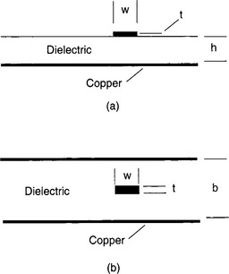
Where a balanced or unbalanced line of quite a short run is required, e.g. between one section of circuitry and another on a printed circuit board, the sort of feeders mentioned above are not convenient. Two alternative types of transmission line are frequently for this purpose; microstrip and stripline. Microstrip consists of a copper track on one side of a printed circuit board, the other side of the board being covered with copper used as a ground plane. The characteristic impedance of such a track− commonly 50Ω− depends upon the thickness of the board and its permitivity, and the width of the track; the thickness of the copper has only a minor second order effect on the characteristic impedance.
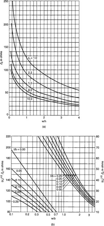
In the case of stripline, the copper trace on the printed circuit board is sandwiched between two ground planes. One is on the reverse of the board, as in microstrip, while the other is on another sheet of single-sided printed circuit material used purely as a ground plane. The two ground planes are pinned together at many points to ensure that they are equipotential surfaces. The construction of both microstrip and stripline is illustrated in Figure 3.7. Graphs giving the characteristic impedance as a function of the dimensions, for both microstrip and stripline are reproduced in Figure 3.8. Note that Figure 3.8b assumes that the stripline conductor is completely immersed in the dielectric. With the commonly employed type of sandwich construction described above, there will be a thin airspace equal to the thickness of the conductor. The effect of this will generally be negligible.
1Signals travel very nearly at the speed of light in an open air-line. In a coax the speed is only about two-third that of light, in delay cable, used for example to feed the Y plates of an oscilloscope, it is much lower still, while in a loaded telephone cable it is only about one twentieth of the speed of light.