Passive circuits
Resistors, capacitors and inductors can be combined for various purposes. When a circuit contains both resistance and reactance, it presents an ‘impedance’ Z which varies with frequency. Thus Z = R + jωL (resistor in series with an inductor) or Z = R - j/(ωC) (resistor in series with a capacitor). The reciprocal of impedance, Y, is known as admittance, so I = E/Z and E = I/Y
At a given frequency, a resistance and a reactance in series Rs and Xs behaves exactly like a different resistance and reactance in parallel Rp and Xp. Occasionally, it may be necessary to calculate the values of Rs and Xs given Rp and Xp, or vice versa. The necessary formulae are given in Appendix 1.
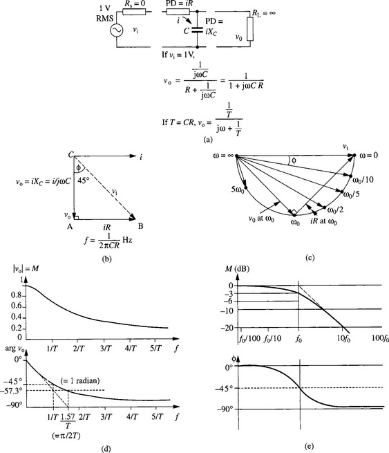
Since the reactance of an inductor rises with increasing frequency, that of a capacitor falls, whilst the resistance of a resistor is independent of frequency, the behaviour of the combination will in general be frequency dependent. Figure 2.1 illustrates the behaviour of a series resistor - shunt capacitor (low pass) combination. Since the current through a capacitor leads the voltage across it by 90° at that frequency (ω0) where the reactance of the capacitor in ohms equals the value of the resistor, the voltage and current relationships in the circuit are as in Figure 2.1b. The relation between vi and vo at ω0 and other frequencies is shown in the ‘circle diagram’ (Figure 2.1c). Figure 2.1d plots the magnitude or modulus M and the phase or argument Φ of vo versus a linear scale of frequency, for a fixed vi. Note that it looks quite different from the same thing plotted to the more usual logarithmic frequency scale (Figure 2.1e).
If C and R in Figure 2.1a are interchanged, a high-pass circuit results, whilst low- and high-pass circuits can also be realized with a resistor and an inductor. All the possibilities are summarized in Figure 2.2. Figure 2.3a shows an alternating voltage applied to a series capacitor and a shunt inductor-plus-resistor, and Figure 2.3b shows the vector diagram for that frequency (fr = 1/2![]() [LC]) where the reactance of the capacitor equals that of the inductor. (For clarity, coincident vectors have been offset slightly sideways.) At the resonant frequency fr, the current is limited only by the resistor, and the voltage across the inductor and capacitor can greatly exceed the applied voltage if XL greatly exceeds R. At the frequency where vo is greatest, the dissipation in the resistor is a maximum, i2R watts (or joules per second), where i is the rms current. The energy dissipated per radian is thus (i2R)/(2πf). The peak energy stored in the inductor is 1/2 LI2 where the peak current I is 1.414 times the rms value i. The ratio of energy stored to energy dissipated per radian is thus
[LC]) where the reactance of the capacitor equals that of the inductor. (For clarity, coincident vectors have been offset slightly sideways.) At the resonant frequency fr, the current is limited only by the resistor, and the voltage across the inductor and capacitor can greatly exceed the applied voltage if XL greatly exceeds R. At the frequency where vo is greatest, the dissipation in the resistor is a maximum, i2R watts (or joules per second), where i is the rms current. The energy dissipated per radian is thus (i2R)/(2πf). The peak energy stored in the inductor is 1/2 LI2 where the peak current I is 1.414 times the rms value i. The ratio of energy stored to energy dissipated per radian is thus ![]() the ratio of the reactance of the inductor (or of the capacitor) at resonance to the resistance. If there is no separate resistor, but R represents simply the effective resistance of the winding of the inductor at frequency f, then the ratio is known as the Q (quality factor) of the inductor at that frequency. Capacitors also have effective series resistance, but it tends to be very much lower than for an inductor: they have a much higher Q. So in this case, the Q of the tuned circuit is simply equal to that of the inductor. Figure 2.3c shows a parallel tuned circuit, fed from a very high source resistance, a ‘constant current generator’. The response is very similar to that shown in Figure 2.3b for the series tuned circuit, especially if Q is high. However, maximum vo will not quite occur when it is in phase with vi unless the Q of the inductor equals that of the capacitor.
the ratio of the reactance of the inductor (or of the capacitor) at resonance to the resistance. If there is no separate resistor, but R represents simply the effective resistance of the winding of the inductor at frequency f, then the ratio is known as the Q (quality factor) of the inductor at that frequency. Capacitors also have effective series resistance, but it tends to be very much lower than for an inductor: they have a much higher Q. So in this case, the Q of the tuned circuit is simply equal to that of the inductor. Figure 2.3c shows a parallel tuned circuit, fed from a very high source resistance, a ‘constant current generator’. The response is very similar to that shown in Figure 2.3b for the series tuned circuit, especially if Q is high. However, maximum vo will not quite occur when it is in phase with vi unless the Q of the inductor equals that of the capacitor.

Figure 2.2 All combinations of one resistance and one reactance, and of one reactance only, and their frequency characteristics (magnitude and phase) and transfer functions (reproduced by courtesy of Electronics and Wireless World)

A tuned circuit passes a particular frequency or band of frequencies, the exact response depending upon the Q of the circuit. Relative to the peak, the −3 dB bandwidth δf is given by δf= ![]() , where f0 is the resonant frequency (see Appendix 4). Where greater selectivity is required than can be obtained from a single tuned circuit, two options are open. Subsequent tuned circuits can be incorporated at later stages in, e.g. a receiver: they may all be tuned to exactly the same frequency (‘synchronously tuned’), or if a flatter response over a narrow band of frequencies is required, they can be slightly offset from each other (‘stagger tuned’). Alternatively, two tuned circuits may be coupled together to provide a ‘band-pass’ response. At increasing offsets from the tuned frequency, they will provide a more rapid increase in attenuation than a single tuned circuit, yet with proper design they will give a flatter pass band. The flattest pass band is obtained with critical coupling; if the coupling is greater than this, the pass band will become double-humped, with a dip in between the peaks. Where the coupling between the two tuned circuits is by means of their mutual inductance M, the coefficient of coupling k is given by
, where f0 is the resonant frequency (see Appendix 4). Where greater selectivity is required than can be obtained from a single tuned circuit, two options are open. Subsequent tuned circuits can be incorporated at later stages in, e.g. a receiver: they may all be tuned to exactly the same frequency (‘synchronously tuned’), or if a flatter response over a narrow band of frequencies is required, they can be slightly offset from each other (‘stagger tuned’). Alternatively, two tuned circuits may be coupled together to provide a ‘band-pass’ response. At increasing offsets from the tuned frequency, they will provide a more rapid increase in attenuation than a single tuned circuit, yet with proper design they will give a flatter pass band. The flattest pass band is obtained with critical coupling; if the coupling is greater than this, the pass band will become double-humped, with a dip in between the peaks. Where the coupling between the two tuned circuits is by means of their mutual inductance M, the coefficient of coupling k is given by
if the inductance of the primary tuned circuit equals that of the secondary. The value of k for critical coupling
if the Q of the primary and secondary tuned circuits is equal. Thus for example, if Qp = Qs = 100 then
So just 1% of the primary flux should link the secondary circuit. Many other types of coupling are possible, some of which are shown in Figure 2.4; Terman [1] gives expressions for the coupling coefficients for these and other types of coupling circuits.

Where a band-pass circuit is tunable by means of ganged capacitors Cp and Cs (Figure 2.4a and b), the coupling will vary across the band. A judicious combination of top and bottom capacitive coupling can give a nearly constant degree of coupling across the band. To this end, the coupling capacitors Cm may be trimmers to permit adjustment on production test. Where Cm in Figure 2.4b turns out to need an embarrassingly small value of trimmer, two small fixed capacitors of 1 pF or so in series may be used, with a much larger trimmer from their junction to ground.
Figure 2.1 showed a simple low-pass circuit. Its final rate of attenuation is only 6 dB/octave and the transition from the pass band to the stop band is not at all sharp. Where a sharper transition is required, a series L in place of the series R offers a better performance. If RL = infinity, Rs = 1.414XL at ω0 (where ω0 = 1![]() LC), the attenuation is 3 dB at ω0, flat below that frequency and tends to − 12 dB/octave above it. If a little peaking in the passband is acceptable (Rs = XL at ω0), there is no attenuation at all at ω0 and the cutoff rate settles down soon after to 12 dB/octave as before. This is an example of a second order Chebychev response. To get an even faster rate of cut-off, especially if we require a flat pass band with no peaking (a Butterworth response), we need a higher order filter. Figure 2.5a shows a third order filter designed to work from a 1 O source into a 1 O load, with a cut-off frequency of 1 rad/s, i.e. 1/2p = 0.159 Hz. (These ‘normalized’ values are not very useful as they stand, but to get to, say, a 2 MHz cut-off frequency, simply divide all the component values by 4p ×06, and to get to a 50 O design divide all the capacitance values by 50 and multiply all the inductance values by 50. Thus starting with normalized values you can easily modify the design to any cut-off frequency and impedance level you want.) The values in round brackets are for a Butterworth design and those in square brackets for a 0.25 dB Chebychev design, i.e. one with a 0.25 dB dip in the pass band. Note the different way that Butterworth and Chebychev filters are specified: the values shown will give an attenuation at 0.159 Hz of 3 dB for the Butterworth filter, but a value equal to the pass-band ripple depth (-0.25 dB for the example shown) for the Chebychev filter. Even so, the higher order Chebychev types, especially those with large ripples, will still show more attenuation in the stop band than Butterworth types. Both of the filters in Figure 2.5a cut off at the same ultimate rate of 18 dB/octave. However, if they were designed for the same −3 dB frequency, the Chebychev response would show much more attenuation at frequencies well into the stop band, because of its steeper initial rate of cut-off, due to the peaking. Most of the filter types required by the practising RF engineer can be designed with the use of published normalized tables of filter responses [2, 3]. These also cover elliptic filters, which offer an even faster descent into the stop band, if you can accept a limitation on the maximum attenuation as shown in Figure 2.5b. On account of their greater selectivity, for a given number of components, elliptical filter designs are widely used in RF applications. Appendix 10 gives a wide range of designs for elliptic low- and high-pass filters. For details of more specialized filters such as helical resonator or combline band-pass filters, mechanical, ceramic, quartz crystal and SAW filters, etc., the reader should refer to one of the many excellent books dealing specifically with filter technology. However, the basic quartz crystal resonator is too important a device to pass over in silence.
LC), the attenuation is 3 dB at ω0, flat below that frequency and tends to − 12 dB/octave above it. If a little peaking in the passband is acceptable (Rs = XL at ω0), there is no attenuation at all at ω0 and the cutoff rate settles down soon after to 12 dB/octave as before. This is an example of a second order Chebychev response. To get an even faster rate of cut-off, especially if we require a flat pass band with no peaking (a Butterworth response), we need a higher order filter. Figure 2.5a shows a third order filter designed to work from a 1 O source into a 1 O load, with a cut-off frequency of 1 rad/s, i.e. 1/2p = 0.159 Hz. (These ‘normalized’ values are not very useful as they stand, but to get to, say, a 2 MHz cut-off frequency, simply divide all the component values by 4p ×06, and to get to a 50 O design divide all the capacitance values by 50 and multiply all the inductance values by 50. Thus starting with normalized values you can easily modify the design to any cut-off frequency and impedance level you want.) The values in round brackets are for a Butterworth design and those in square brackets for a 0.25 dB Chebychev design, i.e. one with a 0.25 dB dip in the pass band. Note the different way that Butterworth and Chebychev filters are specified: the values shown will give an attenuation at 0.159 Hz of 3 dB for the Butterworth filter, but a value equal to the pass-band ripple depth (-0.25 dB for the example shown) for the Chebychev filter. Even so, the higher order Chebychev types, especially those with large ripples, will still show more attenuation in the stop band than Butterworth types. Both of the filters in Figure 2.5a cut off at the same ultimate rate of 18 dB/octave. However, if they were designed for the same −3 dB frequency, the Chebychev response would show much more attenuation at frequencies well into the stop band, because of its steeper initial rate of cut-off, due to the peaking. Most of the filter types required by the practising RF engineer can be designed with the use of published normalized tables of filter responses [2, 3]. These also cover elliptic filters, which offer an even faster descent into the stop band, if you can accept a limitation on the maximum attenuation as shown in Figure 2.5b. On account of their greater selectivity, for a given number of components, elliptical filter designs are widely used in RF applications. Appendix 10 gives a wide range of designs for elliptic low- and high-pass filters. For details of more specialized filters such as helical resonator or combline band-pass filters, mechanical, ceramic, quartz crystal and SAW filters, etc., the reader should refer to one of the many excellent books dealing specifically with filter technology. However, the basic quartz crystal resonator is too important a device to pass over in silence.

A quartz crystal resonator consists of a ground, lapped and polished crystal blank upon which metallized areas (electrodes) have been deposited. There are many different ‘cuts’ but one of the commonest, used for crystals operating in the range 1 to 200 MHz is the AT cut, used both without temperature control and, for an oscillator with higher frequency accuracy, in an oven maintained at a constant temperature such as +70°C, well above the expected top ambient temperature (an OCXO). Where greater frequency accuracy than can be obtained with a crystal at ambient temperature is required, but the warm-up time or power requirements of an oven are unacceptable, a temperature-compensated crystal oscillator (TCXO) can be used. Here, temperature-sensitive components such as thermistors are used to vary the reverse bias on a voltage-variable capacitor in such a way as to reduce the dependence of the crystal oscillator’s frequency upon temperature.
When an alternating voltage is applied to the crystal’s electrodes, the voltage stress in the body of the quartz (which is a very good insulator) causes a minute change in dimensions, due to the piezo-electric effect. If the frequency of the alternating voltage coincides with the natural frequency of vibration of the quartz blank, which depends upon its size and thickness and the area of the electrodes, the resultant mechanical vibrations are much greater than otherwise. The quartz resonator behaves in fact like a series tuned circuit, having a very high L/C ratio. Despite this, it still displays a very low ESR (equivalent series resistance) at resonance, due to its very high effective Q, typically in the range of 10000 to 1000000. Like any series tuned circuit, it appears inductive at frequencies above resonance and there is a frequency at which this net inductance resonates with C0, the capacitance between the electrodes. Since even for a crystal operating in the MHz range, L may be several henrys and C around a hundredth of one picofarad, the difference between the resonant (series resonant) and the antiresonant (parallel resonance with C0) frequencies may be less than 0.1% (see Appendix 9). A crystal may be specified for operation at series or at parallel resonance and the manufacturer will have adjusted it appropriately to resonate at the specified frequency. Crystals operating at frequencies below about 20 MHz are usually made for operation at parallel resonance, and operated with 30 pF of external circuit capacitance Cc in parallel with C0. Trimming Cc allows for final adjustment of the operating frequency in use. This way, a crystal’s operating frequency may be ‘pulled’, perhaps by as much as one or two hundred parts per million, but the more it is pulled from its designed operating capacitance, the worse the frequency stability is likely to be. Like many mechanical resonators (e.g. violin string, brass instrument), a crystal can vibrate at various harmonics or overtones. Crystals designed for use at frequencies much above 20 MHz generally operate at an overtone such as the 3rd, 5th, 7th or 9th. These are generally operated at or near series resonance. Connecting an adjustable inductive or capacitive reactance, not too large compared to the ESR, in series permits final adjustment to frequency in the operating circuit, but the pulling range available with series operation is not nearly as great as with parallel operation. The greatest frequency accuracy is obtained from crystals using the ‘SC (strain compensated or doubly rotated) cut, although these are considerably more expensive. They are also slightly more difficult to apply, as they have more spurious resonance modes than AT cut crystals, and these have to be suppressed to guarantee operation at the desired frequency.
Quartz crystals are also used in band-pass filters, where their very high Q permits very selective filters with a much smaller percentage bandwidth to be realized than would be possible with inductors and capacitors. Traditionally, the various crystals, each pretuned to its designed frequency, were coupled together by capacitors in a ladder or lattice circuit. More recently, pairs of crystals (‘monolithic dual resonators’) are made on a single blank, the coupling being by the mechanical vibrations. More recently still, monolithic quad resonators have been developed, permitting the manufacture of smaller, cheaper filters of advanced performance.