Attenuators and equalizers
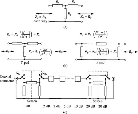
Attenuators, or pads as they are often called, are networks which simulate a lossy transmission line, so that the signal at the output is smaller than at the input, but not changed in any other way. Like a transmission line, they are designed to have a specific characteristic impedance, commonly 50Ω and like a good transmission line their frequency characteristic is flat. Unlike a length of lossy line though, they provide no delay; the path length through an attenuator is ideally zero. A pad exhibiting a resistive impedance R0 at both its input and its output can be realized with three resistors connected in either a ‘Tee’ or a π configuration (see Figure 15.1), which gives design formulae expressed in two different ways. The first gives the hyperbolic design equations for the series and shunt resistors of a Tee pad in terms of the attenuation a in nepers where α = ln(Ein/Eout), i.e. the natural logarithm of the voltage ratio. The second way uses the input/output voltage ratio N where the required attenuation D dB is given by D = 20 log10N. You can thus work out the resistor values for a pad of any attenuation for any characteristic impedance, but for most attenuation values for common characteristic impedances such as 50Ω or 600Ω it is quicker to look up the values in published tables, such as Appendix 3. Note that if the voltage (or current) ratio is very large, then (1) the coupling between input and output circuit must be very small, and (2) looking into the pad from either side we must see a resistance very close to R0 even if the other side of the pad is unterminated. For if very little power crawls out of the far side of the pad, it must mostly be dissipated on this side. Thus when N is very large, (1) Rp in a Tee circuit must be almost zero and Rs in a π circuit almost infinity, and (2) Rs in a Tee circuit will be fractionally less than R0 and Rp in a π circuit fractionally larger than R0. In fact as you can see from Figure 15.1b, the Rs in a Tee circuit is the reciprocal of Rp in a π circuit (in the sense that Rs(Tee)Rp(Pi) = R20) and vice versa, for all values of N. Figure 15.1c shows eight switchable pads arranged to give attenuation in the range 0-60 dB in 1 dB steps. The range can be extended by adding further 20 dB sections, or by adding a 40 dB section. However, in practice the former permits operation up to much higher frequencies, since with attenuations in excess of 20 dB in a single pad, worse errors due to stray capacitance and inductance will be encountered.
A variable attenuator is useful for many measurement applications. Continuously variable attenuators using resistive elements have been designed and produced but are expensive, since three resistors have to be varied simultaneously, with non-linear laws. Continuously variable attenuators working on a rather different principle are readily available at microwave frequencies. Piston attenuators, working on the waveguide beyond cut-off principle are also available for use at V/UHF. Alternatively, attenuators adjustable in 1 dB steps are modestly priced and very useful. For example, if the output of a signal generator is measured with an indicating receiver of some sort, and then an amplifier in series with the attenuator is inserted in the signal path, then when the attenuator is set to provide the same receiver indication as previously, the amplifier’s gain equals the attenuator’s attenuation. The accuracy of the measurement depends only upon that of the variable attenuator, not on the source or detector. The output of the signal generator should not of course be large enough to drive the amplifier into saturation: if, due to limited detector sensitivity, it is necessary to work with a signal level larger than the amplifier can handle, the attenuator can precede rather than follow the amplifier.
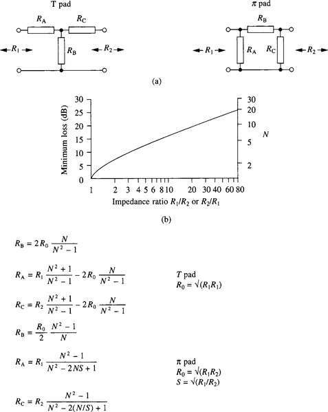
Fixed pads are useful for providing some isolation between stages, albeit at the expense of a power loss. In particular, the use of a pad will reduce the return loss of a poorly matched load seen by a source, or vice versa (see Appendix 3). Sometimes it is desired to connect together two systems with different characteristic impedances, to measure the performance of a 75Ω video amplifier using a 50Ω network analyser, for example. Impedance matching transformers could be used for this purpose, but their frequency range might prove inadequate. A much broader-band solution is to use a pair of ‘mismatch pads’ (a palpable misnomer - they are actually ‘anti-mismatch pads’). A 50Ω to 75Ω pad would be used at the amplifier’s input and a similar pad, the other way round, at its output. Figure 15.2 gives the design formulae for both T and π mismatch pads; note that here N is not the input/output voltage ratio but the square root of the input/output power ratio. For any ratio of impedances to be matched there is a minimum associated loss, e.g. for a pair of 1.5:1 pads (75Ω to 50Ω for example), from Figure 15.2b the loss cannot be less than about 6 dB, unless that is you resort to the use of negative values of resistance in which case you can have a 0 dB mismatch pad or even one with gain. In practice, it is convenient to design the pads for say 10 dB each so that the actual gain of the 75Ω video amplifier mentioned above would be 20 dB greater than the measured value. If the above set-up were being used to measure the stopband attenuation of a 75Ω filter, the extra 20 dB loss of the mismatch pads would undesirably limit the measurement range. In this case it would be better to use ‘minloss’ pads. These are L pads, having only two resistors, a series resistor facing the higher impedance interface and a shunt resistor facing the lower.
Whereas an attenuator provides a loss that is independent of frequency and a filter has an attenuation that varies with frequency, a phase equalizer has no attenuation at any frequency. For this reason it is alternatively known as an all-pass filter (APF) and it is used to provide a phase shift that is dependent upon frequency. A typical application is in a digital phase modulation system where an LC or (more usually) active RC low-pass filter is used at baseband prior to the modulation stage, to limit the bandwidth of transmitted signal. An APF can be used to correct the phase distortion introduced by the baseband filter. The aim is to make the phase shift through the filter/equalizer combination linearly proportional to frequency: when this ‘constant group delay’ condition is met, all frequency components of the digital data stream suffer the same time delay and so their relative phase is unaffected, avoiding ISI (intersymbol interference) in the transmitted signal. The overall link filtering function is usually split equally between the transmitter and the receiver, to obtain the best trade-off between OBW (occupied bandwidth) of the transmitted signal and noise bandwidth at the receiver. However, all of the corresponding equalization may be carried out at one end of the link, say the transmitter, if convenient. A first order phase equalizer provides a phase shift which increases from zero at 0 Hz to 180° at frequencies much higher than its designed 90° centre frequency, the phase variation versus frequency being of a fixed shape. A second order section provides a phase shift which increases from zero at 0 Hz to 360° at frequencies much higher than its designed 180° centre frequency; the rapidity of phase change in the region of the centre frequency being a variable at the disposal of the designer. An equalizer having a number of sections will usually be necessary to equalize the baseband filter. Both firstand second-order APF sections are described in Reference 1. Phase equalization is not necessary if the baseband filter has a constant group delay, i.e. phase shift proportional to frequency throughout the pass band. Among LC filters, the best known design possessing this property is the Bessel filter, but its rate of cut-off is too gradual to provide the desired degree of bandwidth limitation. Linear phase filters with a sharp cut-off at the band edge can be realized using capacitors and inductors [2] by adopting a non-minimum phase design. Reference 3 describes how a low-pass version of such a filter can be realized using an active RC approach. Finite impulse response (FIR) filters exhibit an inherently linear phase/frequency characteristic and they are available either in DSP (digital signal processing) implementations, or as charge-coupled devices.
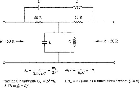
It was mentioned in an earlier chapter that a double balanced mixer used as the first mixer in a high grade receiver should ideally see a broadband 50 O termination at each of its three ports. Often it is not possible to arrange for this desirable state of affairs, but it can be approached. The local oscillator port can be driven by an amplifier with a broadband resistive output and it may prove possible to drive the RF port from a lowgain buffer amplifier to isolate it from the large out-of-band VSWR of the RF band-pass filter. A broadband match at the IF port is more difficult to achieve but it can be approximated by a frequency selective constant resistance network. Such networks have many uses, a familiar domestic example being the cross-over network used to direct the low frequency and high frequency parts of the output of a hi-fi system to the woofer or the tweeter respectively. Figure 15.3 shows a constant resistance band-pass filter network which preserves a constant 50Ω resistive characteristic at both input and output port in its stop bands. The pass band is centred on frequency f = {2π![]() }−1 and the higher the L/C ratio, the narrower the pass band. However, the higher the value of inductance used, the higher the required Q if the pass band loss is to be kept low. Assuming the pass-band loss is low the network is transparent in its pass band, so that the VSWR at its input is simply that of the load on the network’s output. If this is an IF crystal roofing filter, the input VSWR of the network plus roofing filter will be low in the latter’s pass band, but will rise at greater frequency offsets, until it finally falls again in the stop band of the constant resistance network. The poor VSWR immediately either side of the crystal filter’s pass band is unfortunate, but the arrangement is still a considerable improvement upon a direct connection of the crystal filter to the mixer. Alternatively, a high reverse isolation buffer amplifier with low return loss at both input and output ports may be interposed between the constant resistance network and the crystal roofing filter. The latter now sees a good match at all frequencies, both in and out of band. The constant resistance band-pass filter protects the buffer amplifier from the welter of out-of-band signals at the mixer’s output port, while the latter is now correctly terminated at all frequencies.
}−1 and the higher the L/C ratio, the narrower the pass band. However, the higher the value of inductance used, the higher the required Q if the pass band loss is to be kept low. Assuming the pass-band loss is low the network is transparent in its pass band, so that the VSWR at its input is simply that of the load on the network’s output. If this is an IF crystal roofing filter, the input VSWR of the network plus roofing filter will be low in the latter’s pass band, but will rise at greater frequency offsets, until it finally falls again in the stop band of the constant resistance network. The poor VSWR immediately either side of the crystal filter’s pass band is unfortunate, but the arrangement is still a considerable improvement upon a direct connection of the crystal filter to the mixer. Alternatively, a high reverse isolation buffer amplifier with low return loss at both input and output ports may be interposed between the constant resistance network and the crystal roofing filter. The latter now sees a good match at all frequencies, both in and out of band. The constant resistance band-pass filter protects the buffer amplifier from the welter of out-of-band signals at the mixer’s output port, while the latter is now correctly terminated at all frequencies.
References
1. 128-150, Hickman, I. Analog Electronics, Oxford, Heinemann Newnes, 1990.
2. March, Lerner, R.M. Band-pass filter with linear phase. Proceedings of the I.E.E.E., 1964:249–268.
3. 15 February, Delagrange, A. Bring Lerner filters up to date: Replace passive components with op-amps. Electronic Design 1979;4:94–98.