Distortion in power amplifiers, Part VI: the remaining distortions
The previous two chapters considered closely the distortion produced by amplifier output stages: a basically conventional but well designed Class-B amplifier with proper precautions taken against the various sources of nonlinearity can produce insignificant levels of distortion. That which is generated is mainly due to the difficulty of reducing high order crossover nonlinearities with negative feedback that has declining effectiveness with frequency. For 8 Ω loads this is the major source of distortion. For convenience, I have chosen to call such a device a blameless amplifier.
Distortion 3: quiescent current control
An optimised amplifier requires minimisation of output stage gain irregularities around the crossover point by holding the quiescent current Iq at its optimal value. Increasing Iq to move into Class-AB makes the distortion worse, not better, as gm -doubling artifacts are generated.
The initial setting of quiescent current is simple, given a distortion analyser to get a good view of the residual; keeping that setting under varying operating conditions is a much greater problem because Iq depends on small voltages established across low value resistors by power devices with thermally dependant Vbe drops.
How accurately does quiescent current need to be maintained? I wish I could be more specific on this. Some informal experiments with Blameless CFP type outputs at 1 kHz indicate that crossover artifacts on THD residual seem to stay at roughly the same level, partly submerged in the noise, over an Iq range of about 2:1, the centre of this region being around 20 mA. Results may well be different for emitter follower type outputs.
This may seem a wide enough target, but given that junction temperature of power devices may vary over a 100 ° C range, this is not so. Some kinds of amplifier (e.g. current dumping types) manage to evade the problem altogether, but in general the solution is thermal compensation: the output stage bias voltage is set by a temperature sensor (usually a Vbe multiplier transistor) coupled as closely as possible to the power devices.
There are inherent inaccuracies and thermal lags in this sort of arrangement leading to programme dependency of Iq. A sudden period of high power dissipation will begin with the bias current increasing above optimum, as the junctions will heat up very quickly. Eventually the thermal mass of the heatsink will respond, and the bias voltage will be reduced. When the power dissipation falls again, the bias voltage will now be too low to match the cooling junctions and the amplifier will be under biased, producing crossover spikes that may persist for some minutes. This is well illustrated in an important paper by Sato.1
Emitter follower outputs
The major drawback of emitter follower output stages is thermal stabilisation. This can cause production problems in initial setting up since any drift of quiescent current will be very slow as a lot of metal must warm up.
For EF outputs, the bias generator must attempt to establish an output bias voltage that is a summation of four driver and output Vbe’s. These do not vary in the same way. It seems at first a bit of a mystery how the EF stage, which still seems to be the most popular output topology, works as well as it does. The probable answer is Figure 1, which shows how driver dissipation (averaged over a complete cycle) varies with peak output level for the three kinds of EF output, and for the CFP configuration. The Spice simulations used to generate this graph used a triangle waveform to give a slightly closer approximation to the peak-average ratio of real waveforms. The rails were ± 50 V, and the load 8 Ω.

It is clear that the driver dissipation for the EF types is relatively constant with power output, while the CFP driver dissipation, although generally lower, varies strongly. This is a consequence of the different operation of these two kinds of output. In general, the drivers of an EF output remain conducting to some degree for most or all of a cycle, although the output devices are certainly off half the time.
In the CFP, however, the drivers turn off almost in synchrony with the outputs, dissipating an amount of power that varies much more with output. This implies that EF drivers will work at roughly the same temperature, and can be neglected in arranging thermal compensation; the temperature dependent element is usually attached to the heatsink to compensate for the junction temperature of the output devices alone. The Type I EF output keeps its drivers at the most constant temperature.
The above does not apply to integrated Darlington outputs, with drivers and assorted emitter resistors combined in one ill-conceived package where the driver sections are directly heated by the output junctions. This works directly against quiescent stability.
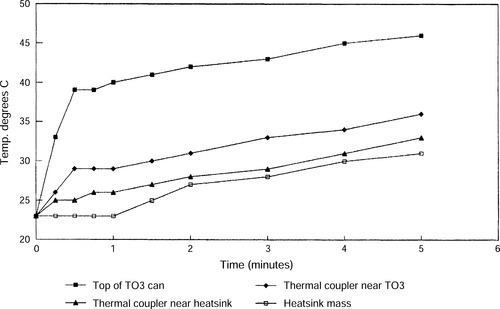
The drawback with most thermal compensation schemes is the slow response of the heatsink mass to thermal transients. The obvious solution is to find some way of getting the sensor closer to one of the output junctions. If TO3 devices are used, then the flange on which the actual transistor is mounted is as close as one can get without a hacksaw. This is however clamped to the heatsink, and almost inaccessible, though it might be possible to hold a sensor under one of the mounting bolts. A simpler solution is to mount the sensor on the top of the TO3 can. This is probably not as accurate an estimate of junction temperature as the flange would give, but measurement shows the top gets much hotter much faster than the heatsink mass, so while it may appear unconventional, it is probably the best sensor position for an EF output stage.
Figure 2 shows the results of an experiment designed to test this. A TO3 device was mounted on a thick aluminium L-section thermal coupler in turn clamped to a heatsink; this construction represents many typical designs. Dissipation equivalent to 100 W/8 Ω was suddenly initiated, and the temperature of the various parts monitored with thermocouples. The graph clearly shows that the top of the TO3 responds much faster, and with a larger temperature change, though after the first two minutes the temperatures are all increasing at the same rate. The whole assembly took more than an hour to asymptote to thermal equilibrium.
The CFP output
In the CFP configuration, the output devices are inside a local feedback loop, and play no significant part in setting Iq, which is affected only by thermal changes in the drivers’ Vbe. Such stages are virtually immune to thermal runaway; I have found that assaulting the output devices with a powerful heat gun induces only insignificant Iq changes. Thermal compensation is mechanically simpler as the Vbe multiplier transistor is simply mounted on one of the driver heatsinks, where it aspires to mimic the driver junction temperature. It is now practical to make the bias transistor of the same type as the drivers, which should give the best matching of Vbe, though how important this is in practice I wouldn’t like to say.2
Because driver heatsinks are much smaller than the main heatsink, the thermal compensation time constant is now measured in tens of seconds rather than tens of minutes, and should give much shorter periods of non optimal quiescent current than the EF output topology.
Distortion 4: nonlinear loading of the voltage amplifier stage by the nonlinear impedance of the output stage
This distortion mechanism was examined in Chapter 18 from the point of view of the voltage amplifier stage (VAS). Essentially, since the VAS provides all the voltage gain, its collector impedance tends to be made high. This renders it vulnerable to nonlinear loading unless it is buffered.
Making a linear VAS is most easily done by applying a healthy amount of local negative feedback via the dominant pole Miller capacitor, and if VAS distortion needs further reduction, then the open loop gain of the VAS stage must be raised to increase this local feedback. The direct connection of a Class-B output can make this difficult for, if the gain increase is attempted by cascoding with intent to raise the impedance at the VAS collector, the output stage loading will render this almost completely ineffective. The use of a VAS buffer eliminates this effect.
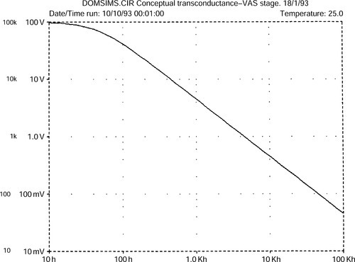
As explained previously, the collector impedance, while high at LF compared with other circuit nodes, falls with frequency as soon as Cdom starts to take effect, and so the fourth distortion mechanism is usually only visible at LF. It is also masked by the increase in output stage distortion above dominant pole frequency P1 as the amount of global NFB reduces.
The fall in VAS impedance with frequency is demonstrated in Figure 3, obtained from the Spice conceptual model outlined previously, with real life values. The LF impedance is basically that of the VAS collector resistance, but halves with each octave once P1 is reached. By 3 kHz it is down to 1 kΩ and still falling. Nevertheless, it can remain high enough for the input impedance of a Class-B output stage to significantly degrade linearity, the actual effect being shown in Figure 4.

An alternative to cascoding for VAS linearisation is to add an emitter follower within the VAS local feedback loop, increasing the local NFB factor by raising effective beta rather than the collector impedance. Preliminary tests show that as well as providing good VAS linearity, it establishes a lower VAS collector impedance across the audio band. It should be more resistant to this type of distortion than the cascode version.
Figure 5 confirms that the input impedance of a conventional EF Type I output stage is anything but linear; the data is derived from a Spice output stage simulation with optimal Iq. Even with an undemanding 8 Ω load, the impedance varies by 10:1 over the output voltage swing. Interestingly, the Type II EF output (using a shared drive emitter resistance) has a 50% higher impedance around crossover, but the variation ratio is rather greater. CFP output stages have a more complex variation that includes a precipitous drop to less than 20 kΩ around the crossover point. With all types under biasing produces additional sharp impedance changes at crossover.

Distortion 5: supply ground loops
Virtually all amplifiers include some form of rail decoupling apart from the main reservoir capacitors; this is usually required to improve HF stability. The standard decoupling arrangements include small to medium sized electrolytics (say 10–1000 μF) connected between each rail and ground, and an inevitable consequence is that voltage variations on the rails cause current to flow into the ground connection chosen. This is just one mechanism that defines the power supply rejection ratio (PSRR) of an amplifier, but it is one that can do serious damage to linearity. If we assume a simple unregulated power supply, (and there are excellent reasons for using such a supply3) then these rails have a significant A.C. impedance and superimposed voltage will be due to amplifier load currents as well as 100 Hz ripple. In Class-B, these supply rail currents are halfwave rectified sine pulses with strong harmonic content, and if they contaminate the signal, then distortion will degrade badly. A common route for interaction is via decoupling grounds shared with input or feedback networks, and a completely separate decoupler ground usually effects a total cure. This point is easy to overlook, and attempts to improve amplifier linearity by labouring on the input pair, VAS, etc., are doomed to failure unless this distortion mechanism is eliminated first.
As a rule it is simply necessary to take the decoupling ground separately back to the ground star point, as shown in Figure 6. Note that the star point A is defined on a short spur from the heavy connection joining the reservoirs; trying to use B as the star point will introduce ripple due to the large reservoir charging current pulses passing through it.
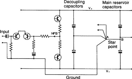
Figure 7 shows the effect on an otherwise optimised amplifier delivering 60 W/8 Ω with 220 μF rail decoupling capacitors. At 1 kHz distortion has increased by more than ten times, which is quite bad enough. However, at 20 Hz the THD has increased at least 100 fold, turning a very good amplifier into a profoundly mediocre one with a single misconceived connection.

If the residual on the supply rails is examined, the ripple amplitude will usually be found to exceed the pulses due to Class-B signal current, and so some of the ‘distortion’ on the upper curve of the plot is actually due to ripple injection. This is hinted at by the phase crevasse at 100 Hz, where ripple partly cancelled the signal at the instant of measurement. Below 100 Hz the – curve rises as greater demands are made on the reservoirs, the signal voltage on the rails increases, and so more distorted current is forced into the ground system.
Generally, if an amplifier is made free from ripple injection under drive conditions, shown by a THD residual without ripple components, there will be no distortion from the supply rails and the complications and inefficiency of high current rail regulators are unnecessary.
There has been much discussion of PSRR induced distortion in EW + WW recently, led by Ben Duncan4 and Greg Ball.5 I part company with Ben Duncan on this issue where he assumes that a power amplifier is likely to have 25 dB PSRR, making expensive high power DC regulators the only answer. He agrees that this sort of PSRR is highly unlikely with the relatively conventional amplifier topologies I have been considering.6
Greg Ball also initially assumes that a power amp has the same PSRR characteristics as an op-amp, i.e. falling steadily at 6 dB/octave. There is absolutely no need for this to be so, given a little RC decoupling, and Ball states at the end of his article that ‘a more elegant solution … is to depend on a high PSRR in the amplifier proper.’
Power supply rejection
For low noise and distortion, all the obvious methods of rail injection must be attended to as a matter of routine. I therefore give here some guidelines that I have found effective with unregulated supplies:
• The input pair must have a tail current source. A tail made of two resistors decoupled mid way is simply not adequate.
• This tail source will probably be biased by a pair of diodes or a led fed from a resistor to ground. This resistor should be split and the midpoint decoupled with an electrolytic of about 10 μF to the appropriate rail.
• If a cascode transistor is used in the VAS, then its base will need to be biased about 1.2 V above whichever rail the VAS emitter sits on; if this is implemented with a pair of diodes then further decoupling seems unnecessary.
• Having taken care of the above, the PSRR will now be limited by injection from the negative rail by a mechanism that is not yet fully clear. RC decoupling can however reduce this to negligible levels.
This is not the whole story on power rail rejection, but it does provide a starting point.
Distortion 6: induced output current coupling
This distortion mechanism, like the previous case, stems directly from the Class-B nature of the output stage. Assuming a sine input, the output hopefully carries a good sinewave, but the supply rail currents are halfwave rectified sine pulses, which are quite capable of inductive crosstalk into sensitive parts of the circuit. This can be very damaging to the distortion performance, as Figure 8 shows.

The distortion signal may intrude into the input circuitry, the feedback path, or even the cables to the output terminals. The result is a kind of sawtooth on the distortion residual that is very distinctive, an extra distortion component which rises at 6 dB/octave with frequency.
This effect appears to have been first publicised by Cherry,7 in a paper that deserves much more attention than it appears to have got. Having examined many power amplifiers, I feel that this effect is probably the most widespread cause of unnecessary distortion.
Effects of this distortion mechanism can be reduced below the measurement threshold by taking care over supply rail cabling layout relative to signal leads, and avoiding loops that will induce or pick up magnetic fields. There are no precise rules for layout that would guarantee freedom from rail induction since each amplifier has its own physical layout and the cabling topology needs to take this into account. All I can do is give guidelines:
• Firstly, implement rigorous minimisation of loop area in the input and feedback circuitry; keep each signal line as close to its ground return as possible.
• Secondly, minimise the ability of the supply wiring to create magnetic fields.
• Thirdly, put as much distance between these two areas as you can. Fresh air beats shielding.
on price every time. Figure 9(a) shows one straightforward approach to tackling the problem; the supply and ground wires are tightly twisted together to reduce radiation. In practice this doesn’t seem too effective for reasons that are not wholly clear, but appear to involve the difficulty of ensuring exactly equal coupling between three twisted conductors.

In Figure 9(b), the supply rails are twisted together but kept well away from the ground return. This allows field generation, but if currents in the two rails butt together to make a sinewave at the output, they should do the same when the magnetic fields from each rail sum. There is an obvious risk of interchannel crosstalk with this approach in a stereo amplifier, but it does seem to deal most effectively with the induced distortion problem.
Distortion 7: nonlinearity from incorrect NFB connection point
Negative feedback is a powerful technique and must be used with care. Designers are repeatedly told that too much feedback can affect slew rate. Possibly true, though the greater danger is that an excess amplifier may produce tweeter-frying HF instability.
However, there is another and more subtle danger. Class-B output stages are a hotbed of high amplitude halfwave rectified currents, and if the feedback takeoff point is even slightly asymmetric, these will contaminate the feedback signal making it an inaccurate representation of the output voltage. This will manifest itself as distortion, Figure 10.

At the current levels in question, all wires and PCB tracks must be treated as resistances, and it follows that point C is not at the same potential as point D whenever TR1 conducts. If feedback is taken from D, then a clean signal will be established here, but the signal at output point C will have a half wave rectified sinewave added to it, due to the resistance C–D. The output will be distorted but the feedback loop will do nothing about it as it does not know about the error.
Figure 11 shows the practical result for an amplifier driving 100 W into 8 Ω, with the extra distortion shadowing the original curve as it rises with frequency. Resistive path C–D that did the damage was a mere 6 mm length of heavy gauge wirewound resistor lead.
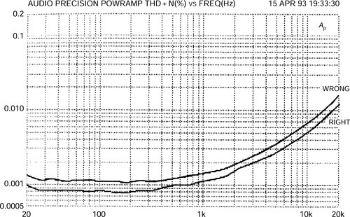
Elimination of this distortion is easy, once you know the danger. Connecting the feedback arm to D is not advisable as it will not be a mathematical point, but will have a physical extent inside which the current distribution is unknown. Point E on the output line is much better, as the half wave currents do not flow through this arm of the circuit.