
Trimodal audio power, Part II
The same components that dominate amplifier noise performance also determine the output d.c. offset; if R9 is reduced to minimise the source resistance seen by Tr3, then the value of R8 is scaled to preserve the same closed-loop gain, and this reduces the voltage drops caused by input transistor base currents.
My previous amplifier designs assumed that a ± 50 mV output d.c. offset is acceptable. This allowed d.c. trimming, offset servos, etc. to be greatfully dispensed with. However, it is not in my nature to leave well enough alone, and it could be argued that ± 50 mV is on the high side for a top-flight amplifier. For this reason, I have reduced this range as much as possible without resorting to a servo; the required changes were already made when impedance of the feedback network was reduced to minimise Johnson noise. There were details on this in Part I of this article.
With the usual range of component values, the d.c. offset is determined not so much by input transistor Vbe mismatch, which tends to be only 5 mV or so, but more by a second mechanism – imbalance in beta. This causes imbalance of base currents, Ib, drawn thorough input bias resistor R1 and feedback resistor R8. Cancellation of the voltage-drops across these components is therefore compromised.
A third source of d.c. offset is non-ideal matching of input degeneration resistors R2,3. Here they are 100 Ω, with 300 mV dropped across each, so two 1% components at opposite ends of their tolerance bands could give a maximum offset of 6 mV. In practice, it is unlikely that the error from this source will exceed 2 mV.
There are several ways to reduce d.c. offset. Firstly, a class-a amplifier with a single output pair must be run from modest ht rails, so the requirement for high-Vce input transistors is relaxed. This allows higher beta devices to be used, directly reducing Ib. The 2SA970 devices used in this design have a beta range of 350 to 700, compared with 100 or less for MPSA06/56. Note the pinout is not the same.
In chapter 26, we reduced the impedance of the feedback network by a factor of 4.5, and the offset component due to Ib imbalance is reduced by the same ratio. We might therefore hope to keep the d.c. output offset for the improved amplifier to within ± 15 mV without trimming or servos. Using high-beta input devices, the Ib errors did not exceed ± 15 mV for ten sample pairs – not all from the same batch – and only three pairs exceeded ± 10 mV. Errors in Ib are now reduced to the same order of magnitude as Vbe mismatches, and so no great improvement can be expected from further reduction of circuit resistances. Drift over time was measured at less than 1 mV, and this seems to be entirely a function of temperature equality in the input pair.
Figure 1 shows the ideal d.c. conditions in a perfectly-balanced input stage, assuming a β of 400, compared with a set of real voltages and currents from the prototype amplifier. In the latter case, there is a typical partial cancellation of offsets from the three different mechanisms, resulting in a creditable output offset of − 2.6 mV.

Biasing for three modes
Figure 2 shows a simplified rendering of the Trimodal biasing system; the full version appears in Figure 3. The voltage between points A and B is determined by one of which can be in command at a time. Since both are basically shunt voltage regulators sitting between A and B, the result is that the lowest voltage wins. The novel Class-A current-controller introduced in the original article1 is used here adapted for 0.1 Ω emitter resistors, mainly by reducing the reference voltage to 300 mV, which gives a quiescent current (Iq) of 1.5 A when established across the total emitter resistance of 0.2 Ω.
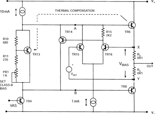
In parallel with the current-controller is the Vbe multiplier Tr13. In Class-B mode, the current-controller is disabled, and critical biasing for minimal crossover distortion is provided in the usual way by adjusting preset Pr1 to set the voltage across Tr13. In Class-A/AB mode, the voltage Tr13 attempts to establish is increased (by shorting out Pr1) to a value greater than that required for Class-A. The current-controller therefore takes charge of the voltage between X and Y, and unless it fails Tr13 does not conduct. Points A B X Y are the same circuit nodes as in reference 1.
Class A/AB mode
In Class-A/AB mode, the current-controller, comprising Tr14,15,16 in Figure 2, is active and Tr13 is off, as Tr20 has shorted out Pr1. Transistors Tr15,16 form a simple differential amplifier that compares the reference voltage across R31 with the Vbias voltage across output emitter resistors R16 and R17; as explained in Ref. 1, for Class-A this voltage remains constant despite delivery of current into the load. If the voltage across R16,17 tends to rise, then Tr16 conducts more, turning Tr14 more on and reducing the voltage between A and B. Tr14,15,16 all move up and down with the amplifier output, and so a tail current-source Tr17 is used.
I am aware that the current-controller is more complex than the simple Vbe multiplier used in most Class-B designs. There is an obvious risk that an assembly error could cause a massive current that would prompt the output devices to lay down their lives to save the rail fuses. The tail-source Tr17 is particularly vulnerable because any fault that extinguishes the tail current removes the drive to Tr14, the controller is disabled, and the current in the output stage will be very large. In Figure 2 the Vbe-multiplier Tr13 acts as a safety-circuit which limits Vbias to about 600 mV rather than the normal 300 mV, even if the current-controller is completely non-functional and Tr14 fully off. This gives a ‘quiescent’ of 3A, and I can testify this is a survivable experience for the output devices in the short-term; however they may eventually fail from overheating if the condition is allowed to persist.
There are important points about the current-controller. The entire tail-current for the error-amplifier, determined by Tr17, is syphoned off from the voltage amplifier stage current source Tr5. This must be taken into account when ensuring that the upper output half gets enough drive current.
There must be enough tail current available to turn on Tr14, remembering that most of Tr16 collector-current flows through R15, to keep the pair roughly balanced. If you feel moved to alter the voltage-amplifier stage current, remember also that the base current for driver Tr6 is higher in Class-A than Class-B, so the positive slew-rate is slightly reduced in going from Class-B to A.
I must admit that the details of the voltage reference were rather glossed over in Ref. 1, because space was running out fast. The original amplifier shown last month used a National LM385/1.2, its output voltage fixed at 1.223 V nominal; this was reduced to approx 0.6 V by a 1 k Ω/1kΩ divider.
The circuit also worked well with Vref provided by a silicon diode, 0.6 V being an appropriate bias voltage drop across two 0.22 Ω output emitter resistors. This is simple, and retains the immunity of Iq to heatsink and output device temperatures, but it does sacrifice the total immunity to ambient temperature that a band-gap reference gives.
The LM385/1.2 is the lowest voltage band-gap reference commonly available; however, the voltages shown in Figure 2 reveal a difficulty with the new lower Vbias value and the complementary feedback pair stage; points A and Y are now only 960 mV apart, which does not give the reference room to work in if powered from node A, as in the original circuit.
The solution is to power the reference from the positive rail, via R42,43. The midpoint of these two resistors is boot-strapped from the amplifier output rail by C5, keeping the voltage across R43 effectively constant. Alternatively, a current-source could be used, but this might reduce positive headroom. Since there is no longer a strict upper limit on the reference voltage, a more easily obtainable 2.56 V device could be used providing R30 is suitably increased to 7 kΩ to maintain Vref at 300 mV across R31.
In practice, stability of Iq is very good, staying within 1% for long periods. The most obvious limitation on stability is differential heating of Tr15,16 due to the main heatsink. Transistor Tr14 should also be sited with this in mind, as heating it will increase its beta and slightly imbalance Tr15,16.
Class-B mode
In Class-B mode, the current-controller is disabled, by turning off tailsource Tr17 so Tr14 is firmly off, and critical biasing for minimal crossover distortion is provided as usual by Vbe-multiplier Tr13. With 0.1 Ω emitter resistors Vbias (between X and Y) is approx 10 mV. I would emphasise that in Class-B this design, if constructed correctly, will be as ‘blameless’ as a purpose-built Class-B amplifier. No compromises have been made in adding the mode-switching.
As in the previous Class-B design, the addition of R14 to the Vbe-multiplier compensates against drift of the voltage amplifier stage current-source Tr5. To make an old but much-neglected point, the preset potentiometer should always be in the bottom arm of the V be divider R10,11 because when presets fail it is usually by the wiper going open; in the bottom arm this gives minimum bias voltage, but in the upper arm it would give maximum.
In Class-B, temperature compensation for changes in driver dissipation remains vital. Thermal runaway with the complementary feedback pair is most unlikely, but accurate quiescent setting is the only away to minimise cross-over distortion. Tr13 is therefore mounted on the same small heatsink as driver Tr6. This is often called thermal feedback, but it is no such thing as Tr13 in no way controls the temperature of Tr6; ‘thermal feedforward’ would be a more accurate term.
Switching modes
The dual nature of the biasing system means Class-A/Class-B switching is easily implemented, as in Figure 3. A Class-A amplifier is an uneasy companion in hot weather, and so I was unable to resist the temptation to sub-title the mode switch ‘Summer/Winter’, by analogy with a car air intake.
Switchover is d.c.-controlled, as it is not desirable to have more signal than necessary running around inside the box, possibly compromising inter-channel crosstalk. In Class-A/AB mode, S1 is closed, so Tr17 is biased normally by D5,6, and Tr20 is held on via R33, shorting out present Pr1 and setting Tr13 to safety mode, maintaining a maximum Vbias limit of 600 mV. For Class-B, S1 is opened, turning off Tr17 and therefore Tr15,16 and Tr14. Transistor Tr20 also ceases to conduct, protected against reverse-bias by D9, and reduces the voltage set by Tr13 to a suitable level for Class-B. The two control pins of a stereo amplifier can be connected together, and the switching performed with a single-pole switch, without interaction or increased crosstalk.
Mode-switching affects the current flowing in the output devices, but the output voltage is controlled by the global feedback loop, and switching is completely silent in operation. The mode is switchable while the amplifier is handling audio, allowing some interesting ‘A/B’ listening tests.
It may be questioned why it is necessary to explicitly disable the current-controller in Class-B; Tr13 is establishing a lower voltage than the current-controller which latter subsystem will therefore turn Tr14 off as it strives futilely to increase Vbias. This is true for 8 Ω loads, but 4 Ω impedances increase the currents flowing in R 16,17 so they are transiently greater than the Class-A Iq, and the controller will therefore intermittently take control in an attempt to reduce the average current to 1.5A. Disabling the controller by turning off Tr17 via R44 prevents this.
Supplying power
Regulated supplies are quite unnecessary, and are virtually certain to do more harm than a good unregulated power supply (Figure 4).
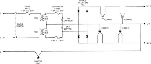
The supply must be designed for continuous operation at maximum current, so the bridge rectifier should be properly heat-sunk, and careful consideration given to the ripplecurrent ratings of the reservoirs. This is one reason why reservoir capacitance has been doubled to 20,000 μF per rail: the ripple voltage is halved, improving voltage efficiency as it is the ripple troughs that determine clipping onset. But the ripple current, although unchanged in total value, is now split between two components. (The capacitance was not increased to reduce ripple injection. This is dealt with far more efficiently and economically by making amplifier psrr high.3)
Do not omit the secondary fuses. Even in these modern times rectifiers do fail, and transformers are horribly expensive.
Test mode
If the Class-A controller is enabled, but preset Pr1 is left in circuit, (e.g. by shorting Tr20 base-emitter) we have a test mode which allows suitably cautious testing; current Iq is zero with the preset fully down, as Tr13 overrides the current-controller, but increases steadily as Pr1 is advanced, until it suddenly locks at the desired quiescent current. If the current-controller is faulty then Iq continues to increase to the defined maximum of 3A.
Thermal design
Class-A amplifiers are hot almost by definition, and careful thermal design is needed if they are to be reliable, and not take the varnish off the Sheraton. Since the internal dissipation of the amplifier is maximal with no signal, simply turning on the prototype and leaving it to idle for several hours will give an excellent idea of worst-case component temperatures. In Class-B the power dissipation is very programme-dependant, and estimates of actual device temperatures in realistic use are notoriously difficult.
Table 1 shows the output power available in the various modes, with typical transformer regulation, etc; the output mode diagram in Part 1, Figure 1, showed exactly how the amplifier changes mode from A to AB with decreasing load resistance. Remember that in this context ‘high distortion’ means 0.002% at 1 kHz. This diagram was produced in the analysis section of PSpice simply by typing in equations, and without actually simulating anything at all.
Table 1
Power capability of the trimodal power amplifier
| W | W | W | Distortion | |
| Load resistance (Ω) | 8 | 6 | 4 | |
| Class A | 20 | 27 | 15 | low |
| Class AB | n/a | n/a | 39 | high |
| Class B | 21 | 28 | 39 | medium |

The most important thermal decision is the size of the heatsink; it is going to be expensive, so there is a powerful incentive to make it no bigger than necessary. I have ruled out fan cooling as it tends to make concern for ultra-low electrical noise look rather foolish; let us rather spend the cost of the fan on extra cooling fins and convect in ghostly silence. The exact thermal design calculations are simple but tedious, with many parameters to enter; the perfect job for a spreadsheet. The final answer is the margin between the predicted junction temperatures and the rated maximum.
Once power output and impedance range is decided, the heatsink thermal resistance to ambient is the main variable to manipulate; and this is a compromise between coolness and cost, for high junction temperatures always reduce semi-conductor reliability, Table 2.
Table 2
Temperature considerations
| Thermal resist°C/W | heat flow W | temp rise°C | temp°C | |
| Juncn to to 3 case | 0.7 | 36 | 25 | 100 junction |
| Case to sink | 0.23 | 36 | 8 | 75 TO3 case |
| Sink to air | 0.65 | 72 | 47 | 67 heatsink |
| Total | 80 | 20 ambient |
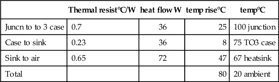
This shows that the transistor junctions will be 80 ° C above ambient, i.e. at around 100 ° C; the rated junction maximum is 200 ° C, but it isn’t wise to get anywhere close to this very real limit. Note the Case-Sink thermal washers are made from high-efficiency material. Standard versions have a slightly higher thermal resistance.
The heatsinks used in the prototype had a thermal resistance of 0.65 ° C/W per channel. This is a substantial piece of metal, and is expensive.
The complete circuit
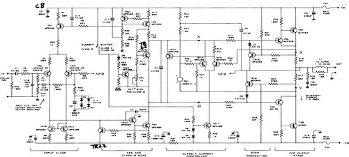
The complete Class-A amplifier is shown in Figure 3, complete with optional input bootstrapping but omitting any balanced-line input amplifier or gain control. The circuitry may look a little complex at first, but we have only added four low-cost transistors to realise a high-accuracy Class-A quiescent controller, and one more to implement mode-switching. Since the biasing system has been described above, only the remaining amplifier subsystems are dealt with here.
The input stage follows my design methodology in running at a high tail current to maximise transconductance, and then linearizing it by adding input degeneration resistors R2,3. These reduce the final transconductance to a suitable level. Current-mirror Tr10,11 forces the collector currents of the two input devices Tr2,3 to be equal, balancing the input stage to prevent the generation of second-harmonic distortion. The mirror is degenerated by R6,7 to eliminate the effects of Vbe mismatches in Tr10,11.
With some misgivings I added the input network R9, C15, which is definitely not intended to define the system bandwidth, unless fed from a buffer stage; with practical values the h.f. roll off could vary widely with the source impedance driving the amplifier. It is intended rather to give the possibility of dealing with rf interference without having to cut tracks. Resistor R9 could be increased for bandwidth definition if the source impedance is known, fixed, and taken into account when choosing R9; bear in mind that any value over 47 Ω will measurably degrade the noise performance. The values given roll off above 150 MHz to keep out uhf.
As a result of insights gained while studying the slewing behaviour of the generic/Lin configuration, I have increased the input-stage tail current from 4 to 6 mA, and increased the voltage amplifier stage standing current from 6 to 10 mA over the original circuit. This increases the maximum positive and negative slew rates from the basic + 21, − 48 V/μs of reference 4 to + 37, − 52 V/μs; as described elsewhere2 this amplifier architecture is always assymetrical in slew rate. One reason is feedthrough in the voltage amplifier current source; in the original circuit an unexpected slew rate limit was set by fast edges coupling through the current source c-b capacitance to reduce the bias voltage during positive slewing. This effect is minimised here by using the negative-feedback type of current source bias generator, with voltage amplifier collector current chosen as the controlled variable.
Transistor Tr21 senses the voltage across R13, and if it attempts to exceed Vbe, turns on further to pull up the bases of Tr1 and Tr5. Capacitor C11 filters the d.c. supply to this circuit and prevents ripple injection from the positive rail. Capacitor C14, with R5, provides decoupling. Increasing input tail-current also mildly improves input-stage linearity, as it raises the basic transistor gm and allows R2,3 to apply more local feedback.
The voltage amplifier stage is linearised by beta-enhancing stage Tr12, which increases the amount of local feedback through Miller dominant-pole capacitor C3, often referred to as Cdom. Resistor R36 has been increased to 2.2 kΩ to minimise power dissipation, as there seems to be no significant effect on linearity or slewing. Do not, however, attempt to omit it altogether, or linearity will be affected and slewing much compromised.
As described in Ref. 3, the simplest way to prevent ripple from entering the voltage amplifier via the negative rail is old-fashioned RC decoupling, with a small R and a big C. We have some 200 mV in hand (Chapter 26) in the negative direction, compared with the positive, and expending this as the voltage-drop through the RC decoupling will give symmetrical clipping. R37 and C12 perform this function; the low rail voltages in this design allow the 1000 μF capacitor C12 to be a fairly compact component.
The output stage is of the complementary feedback pair (CFP) type. As described in Chapter 26, this gives the best linearity and quiescent stability, due to the two local negative feedback loops around driver and output device. Quiescent stability is particularly important with R16,17 as low as 0.1 Ω, and this low value would probably be rather dicey in a double emitter-follower output stage.
Voltage efficiency of the complementary feedback pair is also higher than the emitter follower version. Resistor R25,26 define a suitable quiescent collector current for the drivers Tr6,8, and pull charge carriers from the output device bases when they are turning off. The lower driver is now a BD136; this has a higher fT than the MJE350, and seems to be more immune to odd parasitics at negative clipping.
The new lower values for the output emitter resistors R16,17 halve the distortion in Class-AB. This is equally effective when in Class-A with too low a load impedance, or in Class-B but with Iq maladjusted too high. It is now true in the latter case that too much Iq really is better than too little – but not much better, and AB still comes a poor third in linearity to Classes A and B.
Safe operating area protection is given by the networks around Tr18,19. This is a single-slope safe operating area system that is simpler than two-slope safe area, and therefore somewhat less efficient in terms of snuggling the limiting characteristic up to the true safe operating area of the output transistor. However, in this application, with low rail voltages, maximum utilisation of the transistor safe area is not really an issue; the important thing is to observe maximum junction temperatures in the A/AB mode.
The global negative-feedback factor is 32 dB at 20 kHz, and this should give a good margin of safety against Nyquist-type oscillation. Global negative feedback increases at 6 dB/octave with decreasing frequency to a plateau of around 64 dB, the corner being at a rather ill-defined 300 Hz; this is then maintained down to 10 Hz. It is fortunate that magnitude and frequency here are non-critical, as they depend on transistor beta and other doubtful parameters.
Performance
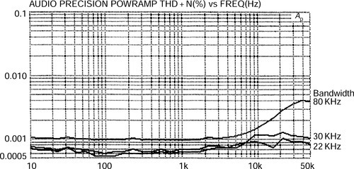
The performance of a properly-designed Class-A amplifier challenges the ability of even the Audio Precision measurement system. To give some perspective on this, Figure 5 shows the distortion of the AP oscillator driving the analyser section directly for various bandwidths. There appear to be internal mode changes at 2 kHz and 20 kHz, causing step increases in oscillator distortion content; these are just visible in the THD plots for Class-A mode.

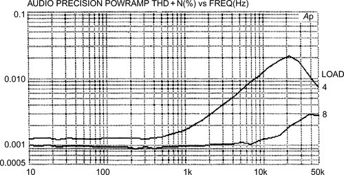
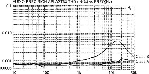
Figure 6 shows Class-B distortion for 20 W into 8 and 4 Ω, while Figure 7 shows the same in Class-A/AB.

I would like to acknowledge the invaluable help and encouragement of Gareth Connor. Credit goes to him for the tricky task of PCB layout – and not me, as previous adverts have implied.
Erratum
Regrettably, a couple of errors crept into the original article on Class-A.1 On page 229, second column: ‘Tr15,16 then compares the reference voltage with that at point Y’ should read ‘at point X’. On page 229, third column: ‘This comes to the same thing as maintaining a constant Vbias across Tr5’ should read ‘across Tr13’. This is nobody’s fault but mine, and I humbly apologise as it cannot have made understanding the current-controller action any easier. (Author’s note: these corrections have been made in this edition.)