
Few compliments for non-complements
A further article by another author, Mr Olsson, also caused me to begin my own investigations, not least because few performance details were given in the original. The concept might have worked, but it did not, so all I could really do was say so, adding some more positive material on two-stage amplifiers in general. They turned out to be rather awkward things.
I want to stress that the last thing intended in these ‘reactive’ articles is discourtesy to the original authors. However, what I do is Science, which is based on Truth, and the latter has proverbially no respect for persons.
Bengt Olsson’s most interesting article on quasi-complementary FET output stages1 prompted me to examine how his proposed configuration works. Investigations showed that his scheme changes not just the output stage but the entire structure of the amplifier, and it presents some intriguing new design problems.
An alternative architecture
Nearly all audio amplifiers use the conventional architecture I have analysed previously.2 There are three stages, the first being a transconductance stage, i.e. differential voltage in/current out, the second is a transimpedance stage i.e. current in/voltage out and lastly a unity-gain output stage, Figure 1(a).
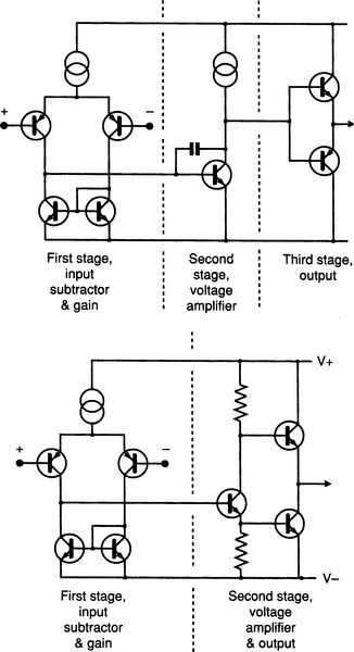
Clearly, the second stage has to provide all the voltage gain and is therefore formally named the voltage amplifier stage (VAS). This architecture has several advantages. A main benefit is that it is straightforward to arrange things so that the interaction between stages is negligible. For example, there is very little signal voltage at the input to the second stage, due to its current-input nature. This results in very little voltage on the first stage output, which in turn minimises phase-shift and possible Early effect.
In contrast, the architecture presented by Olsson is a two stage amplifier, Figure 1(b). The first stage is once more a transconductance stage, though now without a guaranteed low impedance to accept its output current. The second combines voltage amplifier stage and output stage in one block. It is inherent in this scheme that the voltage amplifier must double as a phase-splitter. This results in two dissimilar signal paths to the output, and it is not at all clear that trying to break this block down further will assist a linearity analysis. The use of a phase-splitting stage harks back to valve amplifier days, when it was essential due to the lack of complementary valve technology.
Since the amount of linearising global feedback available depends upon amplifier open-loop gain, the way in which the stages contribute to this is are of great interest. The normal three-stage architecture always has a unity-gain output stage – unless you really want to make life difficult for yourself. As a result the total forward gain is simply the product of the transconductance of the input stage and the transimpedance of the voltage amplifier stage. Transimpedance is determined solely by the Miller capacitor Cdom, except at very low frequencies.3
Typically, the feedback factor at 20 kHz will be 25–40 dB. It will increase at 6 dB per octave with falling frequency until it reaches the dominant pole frequency P1, when it flattens out. What matters for the control of distortion is the amount of negative feedback, NFB, available, rather than the open-loop bandwidth, to which it has no direct relationship.
In my EW + WW Class-B design, input stage gm is about 9 mA/V, and Cdom is 100 pF, giving a feedback factor of 31 dB at 20 kHz. In other designs I have used as little as 26 dB at the same frequency with good results.
Arranging the compensation of a three-stage amplifier can be relatively simple. Since the pole at the voltage-amplifier stage is already dominant, it can be easily increased to lower the h.f. negative-feedback factor to whatever level is considered safe. The local negative feedback working on the voltage amplifier has an invaluable linearising effect. I am aware that some consider there are better ways to perform this sort of compensation, but the Miller approach is so far the most stable method in my experience.
Fewer stages, more complexity?
Paradoxically, a two-stage amplifier may be more complex in its gain structure than a three-stage. Forward gain depends on the input-stage gm, the input-stage collector load, and the gain of the output stage, which will be seen to vary in a most unsettling manner with bias and loading. Input-stage collector loading plays a part here since the input stage cannot be assumed to be feeding a virtual earth.
Choosing the compensation is also more complex for a two-stage amplifier. The voltage-amplifier/phase-splitter has a significant signal voltage on its input. Usually, the pole-splitting mechanism enhances Nyquist stability by increasing the pole frequency associated with the input stage collector. But because of the relatively high voltage on the voltage-amplifier/phasesplitter, the pole-splitting mechanism is no longer effective.
This may be why Olsson’s circuit uses a cascoded input stage comprising Tr6,7 in his original circuit, Figure 11. This presents the input device collectors with a low impedance and prevents a significant collector pole. Another valid reason is that it also allows the use of high-beta low-Vce input transistors, which minimise output d.c. offset due to base current mismatch. This is usually much larger than the d.c. offset due to Vbe mismatch.
Such an input cascode can also improve power-supply rejection as it prevents Early effect from modulating the subtractive action of the input pair.
Simple calculation gives the gm of Olsson’s amplifier as 16 mA/V, but the effective gain of the next stage seems much more difficult to equate. A full PSpice simulation of the complete amplifier with an 8 Ω load shows that the feedback factor is 36 dB up to 300 Hz. It then rolls off at the usual 6 dB/octave, until it passes through OdB at about 20 kHz. This 36 dB represents much less feedback than the three-stage version. It indicates that Cdom, notionally connected between drain and gate of M3, must be comparatively very large at approximately 3 nF.
Specified internal capacitances of M3 are certainly orders of magnitude larger than those of an equivalent bipolar device – they vary from sample to sample and also with operating conditions such as Vds. These unwanted variations would appear to make stable and reliable compensation a difficult business.
The low-frequency feedback factor is about 6 dB less with a 4 Ω load, due to lower gain in the output stage. However, this variation is much reduced above the dominant pole frequency, as there is then increasing local negative feedback acting in the output stage.
Devices and desires
In his opening paragraph, Olsson says that the symmetry of complementary transistor output stages is theoretical rather than practical. Presumably he is referring only to power-fets, as suitable pairs of bipolar devices, such as Motorola MJ802/MJ4502 – old favourites of mine – exhibit excellent symmetry.4 Admittedly, the two devices are not exact mirror-images, but the asymmetries are small enough for even-order harmonic generation in the output stage to be negligible. This is surely what counts.
This symmetry does not hold for power-fets however, and so it may be that some of Olsson’s concern with symmetry flows from an initial decision to use fets. I find it difficult to understand why power fets in particular suffer from so many mis-statements. It is still confidently held that fets are more linear than bipolars, although the opposite is certainly the case when the two types of device are used in normal Class-B output stages.
Similarly, FET robustness is often exaggerated, the devices being prone to summary explosion under serious parasitic oscillation. Mercifully bipolars are not. In particular, I find it hard to understand Olsson’s contention that FET parameters are predictable – they are notorious for being anything but.
From one manufacturer’s data, namely Harris, the Vgs for the IRF240 varies between 2 and 4 V for an Id of 250 μA – a range of two to one. In contrast the Vbe/Ic relation in bipolars is fixed by a mathematical equation for a given transistor type. The exponential relationship may be regarded as more non-linear than the partially-square-law FET Vgs/Id relationship but it is dependable, and gives a much higher transconductance. This can always be traded for linearity by introducing local negative feedback.
Output considerations
Figure 2 shows the basic output configuration I have investigated – I have not examined the ‘anti-saturation’ schemes intended to provide the output fets with extra gate drive.

My first discovery is that the voltage-amplifier stage/phase-splitter does not have to be a FET. Replacing it with a bipolar junction transistor, for example MPSA92, gives almost identical results. I have used M1,2 etc. rather than Tr1,2 for FET designations as this preserves consistency with the PSpice output.
This output stage configuration is totally different in operation from the conventional Class-B stages discussed in Ref. 1. It is a hybrid common-drain/common-source configuration, or, in bipolar speak, a common-collector/common-emitter (cc–ce) stage. In this sort of output, the upper emitter-follower has a common-emitter active-load. This load may or may not deliver an appropriate current into the node it shares with the upper device.
The input-voltage/output-current relationship for the upper and lower devices will be different, as a result of the two dissimilar paths to the output. This means that while such a stage can always be biased into Class-A by increasing the quiescent enough5 there is every likelihood that it will be an inefficient kind of Class-A. It will deviate seriously from the constant-sum-of-currents condition that distinguishes classical Class-A.6
Lower quiescents tend to give a depressingly non-linear and asymmetrical Class-AB. In general there is no equivalent at all to standard Class-B, where the symmetry of the configuration – rather than anything else – allows both output devices to be biased to the edge of conduction simultaneously.
In general, cc–ce stages generate large amounts of even-order distortion, due to their inherent asymmetry. I appreciate however that avoiding this is one of the prime purposes of Olsson’s circuit.
In Figure 2, the position of Vbias causes a form of bootstrapping, and I can confirm that driving it from the output is essential to make the scheme work.
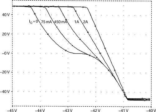
Figure 3 shows drain current in each output FET when driving an 8 Ω load, with Vbias stepped, as simulated by PSpice. Compared with conventional Class-B, the drain currents cross over smoothly. This seems intuitively a good idea, and has been recommended by several writers, but in fact a smooth-looking current crossover does not guarantee a linear composite gain characteristic.

Figure 4 shows the input/output characteristic for the stage. You can see that the lower Vbias levels produce a sigmoidal transfer function, with gain falling off in the cross over region. This gross output distortion is much greater than that given by a normal Class-AB stage. It suggests that it is only practical to run the stage in full Class-A, i.e., the straight line at the right of the plot. I do not recall a mention of this point in the original article.
Quiescent current needed to achieve this is about 2 A. The desirability of Class-A operation is reinforced by the incremental gain plot in Figure 5. It is clear that the gain variations are serious for lower Vbias, and do not augur well for the closed-loop distortion performance. Only the rightmost Class-A gain characteristic has a clear flat portion over its operational range.
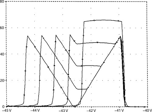
It is true that the drain currents in this stage are symmetrical – but the quiescent required to remove the sharp-eared ‘Batman’ effect in Figure 5 is so high that the amplifier is working entirely in Class-A. The symmetry of the circuit means only that when distortion is produced, it will be predominantly odd-order, which is not normally considered a good thing from the subjective point of view. To keep the stage linear into 4 Ω loads would demand a quiescent of 2.9A. It is interesting that this is not twice the current for the 8 Ω case.
There are other significant differences from the usual voltage-follower configuration, which if nothing else has a stage gain reliably close to unity. Olsson’s output stage gain varies with Vbias adjustment – even when in Class-A – and also varies strongly with load impedance. This would seem to make reliable compensation a difficult business, but in the complete amplifier this variation is probably only significant below the dominant-pole frequency P1.
Figure 6 is a comparison between the Olsson configuration and three conventional stages, all biased to drive an 8 Ω load in Class-A. Traces 1 and 2, at the top, are bipolar-emitter follower and complementary-feedback-pair stages. These produce the usual linearity and close approach to unity gain.

The curved lower trace, 4, is a conventional complementary FET output. Trace 3 is the Olsson stage, with its gain of about 65 times normalised to fit in between the other curves. It shows stronger curvature than the bipolar stages, and despite everything, is actually less symmetrical than the usual output stages. I think this is inherent in the circuit’s lack of symmetry about the output line.
I hope this article is a fair analysis of the proposed configuration, and that I have not made any serious misinterpretations of Mr Olsson’s intentions. I also trust that it will not be taken as purely destructive criticism, for that is not my intention. I have to conclude that the configuration appears to require a very high quiescent current for linear operation, and has only a limited amount of negative feedback available to correct output stage distortions. Any deeper investigation would need to be encouraged by some promise that the Olsson configuration can deliver substantial benefits, and as far as my analysis goes, this does not seem likely.