
Simplified Design Approaches
This chapter is devoted to simplified design approaches for a cross section of data-converter ICs. All of the general design information in Chapters 1 through 3, as well as the specific design information of Chapters 4 through 7, applies to the examples in this chapter. However, each IC has special design requirements, all of which are discussed in detail. The circuits in this chapter represent both classic and state-of-the-art applications. In addition, the circuits can be used immediately the way they are or, with alterations in component values, as a basis for simplified design of similar data converters. If the circuits do not perform as expected (unthinkable), consult the testing and troubleshooting information at the end of Chapter 1.
8.1 References for ADCs and DACs
Although many of the data-converter ICs described in this book have a built-in reference, some require external references (or will work better with a precision external reference). This section is devoted to simplified design of precision, low-drift references.
Even if conversion linearity is perfect, the accuracy of any converter is limited by the temperature drift or long-term drift of the voltage reference. If the voltage reference is allowed to add ½ LSB to the converter, a reference must be reasonably stable even for small temperature variations. When temperature changes are large, the reference accuracy becomes critical. Figure 8-1 shows a comparison of reference requirements for various bit lengths in both data converters and digital panel meters.
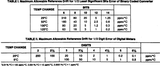
FIGURE 8-1 Comparison of reference requirements for various bit lengths (National Semiconductor, Linear Applications Handbook, 1994, p. 378)
A voltage reference used in a data converter must do several things besides supplying a fixed voltage. First, input power supply changes must be rejected by the reference. The zener used in the reference must be biased properly. (Other parts of the reference circuit scale the zener voltage and provide a low-impedance output.) The reference must reject ambient temperature changes so that the temperature drift of the reference, plus the zener drift, does not exceed the desired drift limit.
Although zener TC (temperature coefficient) is critical to reference performance, other sources of drift can easily add as much error as the zener, even in references with a modest 20 ppm/°C temperature drift or TC. Zener drift and op-amp drift add directly to the drift error. The error of resistors used in the reference circuit is a function of how well the scaling resistors track. (Resistors with a high TC can be used in precision references, if the scaling resistors track each other.)
Figure 8-2 shows the drift-error contribution from various components used in a 10-V reference (with a 6.9-V zener). The drift contribution of resistor mistracking is about 0.4, because the gain is 1.4. Figure 8-2 does not show the contribution of input supply variations. As a guideline, such variations can be ignored if the input is 1% regulated and the resistor feeding the zener is stable to 1%.
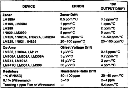
FIGURE 8-2 Drift-error contribution from various components (National Semiconductor, Linear Applications Handbook, 1994, p. 379)
8.1.1 Voltage Reference with 20-ppm/°C Performance
Figures 8-3, 8-4, and 8-5 show three adjustable voltage references, all with a 20-ppm/°C (or better) temperature drift. The following is a summary of the design considerations.
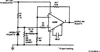
FIGURE 8-3 Voltage reference with zener (National Semiconductor, Linear Applications Handbook, 1994, p. 379)
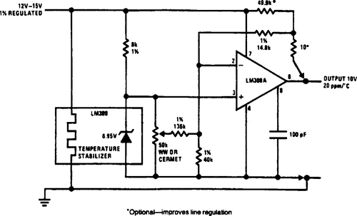
FIGURE 8-4 Voltage reference with temperature stabilizer (National Semiconductor, Linear Applications Handbook, 1994, p. 380)
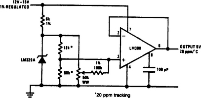
FIGURE 8-5 Voltage reference below zener value (National Semiconductor, Linear Applications Handbook, 1994, p. 380)
In the circuit of Fig. 8-3, an LM308 op amp is used to increase the zener output to 10 V. This combination adds a worst-case drift of 4 ppm/°C to the 10 ppm/°C drift of the zener. Resistors R3 and R4 must track to better than 10 ppm/°C, bringing the total error to about 18 ppm/°C.
Potentiometer R5 and resistor R2 are included so that the output can be adjusted to eliminate the initial zener tolerance. The loading on R5 by R2 is small, and there is no tracking requirement between R5 and R2. However, it is necessary for R2 to track R3/R4 within 50 ppm.
In the circuit of Fig. 8-4, a low-drift reference and op amp are used to give a total drift (exclusive of resistors) of 3 ppm/°C. This relaxes the resistor-tracking requirement to about 50 ppm/°C, allowing ordinary 1% resistors to be used. If the circuit is used in applications requiring 3-ppm/°C to 5-ppm/°C overall drift, tighten the resistor-tracking. For more accurate applications, use Kelvin sensing for both output and ground.
For the lowest possible drift in either circuit (Fig. 8-3 or 8-4), substitute a 1-μV/°C op amp, 1-ppm tracking resistors, and an LM199A, using the components shown in Fig. 8-2. Such combinations can produce overall drifts of 1 ppm/°C. In both circuits, it is important to remember that the tracking of resistors can, at worst case, be twice the temperature drift of either resistance.
The circuit of Fig. 8-5 is used when the reference output is less than the zener voltage. In this case, the reference produces a 5-V output with a 12- to 15-V regulated (1%) input. The zener drift contributes proportionally to the output drift, whereas op-amp-offset drift adds a greater rate. With the 10-V references (Figs. 8-3 and 8-4), 15-μV/°C from the op amp contributes 2 ppm/°C. In the 5-V reference of Fig. 8-5, 15-μV/°C adds 3 ppm/°C. This makes the op-amp choice more important when the output voltage is lowered. Of course, if a high output impedance to the data converter can be tolerated (usually not), the op amp can be eliminated.
8.1.2 Voltage Reference with 1-ppm/°C Performance
Figure 8-6 shows a circuit that can be trimmed to provide 1-ppm/°C (or better) performance. The trimming procedure is as follows. Note that both the 40-k and 14.8-k resistors must be 1 ppm tracking.
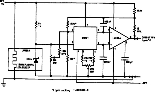
FIGURE 8-6 Voltage reference with 1-ppm/°C performance (National Semiconductor, Linear Applications Handbook, 1994, p. 381)
Disconnect the zener and ground the op-amp input. Null the op-amp offset to zero using the 20-k wire-wound pot. Reconnect the zener, and adjust the circuit output to precisely 10 V (at pin 6 of LM108A) using the 50-k pot. Make a run through the full temperature range and note the drift. The LM121 will drift 3.8-μV/°C for every 1 μV of offset. So for every 5-μV/°C drift at the output, adjust the op amp 1 μV (1.4 μV measured at the circuit output) in the opposite direction with the 20-k pot. Readjust the circuit output to 10 V (50-k pot), and check drift through the full temperature range.
To get the best results, cycle the circuit through the temperature range a few times before making the final test or trimming. This relieves stress on components. Oven testing can sometimes cause thermal gradients across circuits, resulting in 50-μV to 100-μV errors. However, with careful layout and trimming, overall reference drifts of 0.1 to 0.2 ppm/°C are possible.
As always, good single-point grounding is important. Traces on a PC board can easily have 0.1-ohm resistance. Only 10 mA will cause a 1-μV shift. In addition, because these references are close to high-speed digital circuits, shielding might be necessary to prevent pickup at the op-amp inputs. Transient response to pickup, or rapid-loading changes, can sometimes be improved with a large capacitor (1-μf to 10-μF) directly on the op-amp output. Of course, this depends on the op-amp stability.
8.2 Unusual ADC Applications
Figure 8-7 shows an ADC capable of providing solutions to many system-design problems. The following paragraphs summarize typical applications for the ADC.
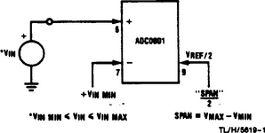
FIGURE 8-7 Basic circuit for arbitrary zero and span (National Semiconductor, Linear Applications Handbook, 1994, p. 465)
8.2.1 Accommodating Arbitrary Zero and Span
In many systems, the analog signal to be converted does not range fully to ground (0.00 VDC), nor does the signal reach up to the full supply or reference-voltage value. This presents two problems for ADCs. First, a zero-offset is needed, and this offset might be in volts rather than the usual few millivolts provided. Second, the full-scale must be adjusted to accommodate this reduced span. (Span is the actual range of the analog input signal from Vin MIN to Vin MAX.)
When Vin equals Vin MIN, the differential input to the ADC is 0V, and a digital-output code of 0 is produced. When Vin equals Vin MAX, the differential input to the ADC is equal to the span. In the ADC of Fig. 8-7, there is an internal gain of two for the voltage, which is applied to pin 9 (the Vref/2 input). This makes it possible to adjust the ADC to provide digital full scale and thus accommodate a wide range of analog-input voltages.
8.2.2 Analog Inputs Less Than Complete Supply Range
Figure 8-8 shows the ADC operating with a ratiometric transducer, which outputs 15% to 85% of the full 5-V supply (VCC). The transducer output is applied to Vin (+), with 15% of VCC (0.75 V) applied to Vin (-). The Vref/2 pin is biased at one-half of the span, or ½ 85% – 15%), or 35% of the supply (1.75 V) through a unity-gain op amp. This circuit configuration can provide 9-bit performance with an 8-bit converter, if the span of the analog input uses only one-half of the available 0-V to 5-V span. (This would be a span of about 2.5 V, which could start anywhere over the range of 0 V to 2.5 V.)
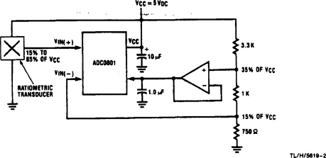
FIGURE 8-8 Operating with a ratiometric transducer (National Semiconductor, Linear Applications Handbook, 1994, p. 465)
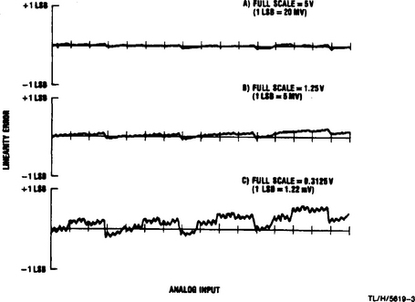
Note that linearity error increases when the analog-input span is reduced. This is shown in Fig. 8-9, which gives a comparison of three full-scale values (A = 5 V, B = 1.25 V, and C = 0.3125 V). Of course, resolution increases when the span is reduced. For example, when full scale is 5 V, 1 LSB is 20 mV, and the resolution is 8 bit. With full scale at 1.25 V, 1 LSB = 5 mV, and resolution is 10 bit. When full scale is reduced to 0.3125 V, 1 LSB is 1.22 mV, and resolution is 12 bit.
8.2.3 10-Bit Resolution from 8 Bits
Figure 8-10 shows the basic connections to produce 10-bit resolution from the 8-bit ADC. The two extra bits are provided by the 2-bit external DAC (the resistor string) and the analog switch SW1. With these connections the Vref/2 pin is supplied with 1/8 Vref so that each of the four spans encoded will be 2 × 1/8 Vref = ¼ Vref.
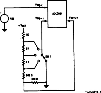
FIGURE 8-10 Basic connections for 10-bit resolution from 8-bit ADC (National Semiconductor, Linear Applications Handbook, 1994, p. 467)
In a practical circuit, the switch is replaced by an analog multiplexer (such as a classic CD4066 quad bilateral switch), and a microprocessor is programmed to do a binary search for the two MS bits. These two bits plus the 8 LSBs provided by the ADC result in the 10-bit data. This basic idea can be simplified to a 1-bit ladder to cover a particular range of analog input voltages with increased resolution.
8.2.4 Direct Encoding of Low-Level Signals
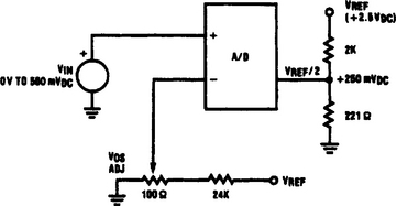
Figure 8-11 shows the ADC0801 connected to encode low-level signals without an external op amp. The Vin (–) input is used as an offset adjustment. When the analog input applied at Vin (+) is at 0 V, the 8-bit digital output is at all 0s. All 1s are output by the ADC when the analog input is at 500 mV.
8.2.5 Digitizing a Current Flow
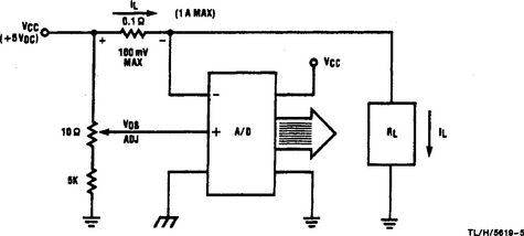
Figure 8-12 shows the ADC0801 connected to provide a digital output that corresponds to a load current. This is done by sampling the load current with a 0.1-ohm resistor connected between VCC and the load. The voltage produced across the resistor is monitored at the Vin (–) input. The Vin (+) input is used as the offset adjustment. When the load current is 0, the digital output is at all 0s. All 1s are output by the ADC when the load current is 1 A. (Do not exceed 100 mV across the load-sampling resistor.)
8.3 Data Acquisition with ADCs
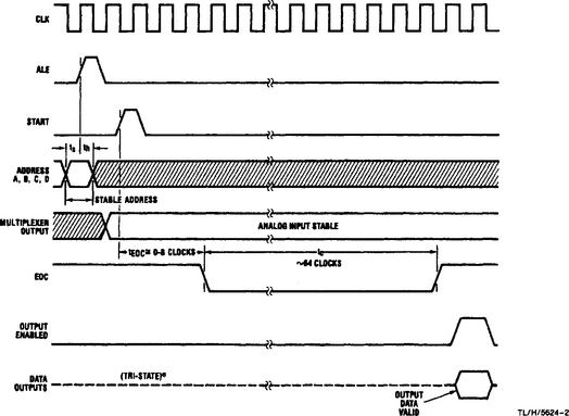
Figure 8-13 shows ADCs specifically designed for data-acquisition applications. Figures 8-14 and 8-15 show the analog input-selection code and timing diagram, respectively. The ADC0816 and ADC0817, CMOS 16-channel data-acquisition devices are actually selectable multi-input 8-bit ADCs. However, in addition to a standard 8-bit SAR-type ADC, these devices also contain a 16-channel analog multiplexer (MUX) with 4-bit latched address inputs. As a result, the ICs include much of the circuitry required to build an 8-bit accurate, medium-throughput data-acquisition system.
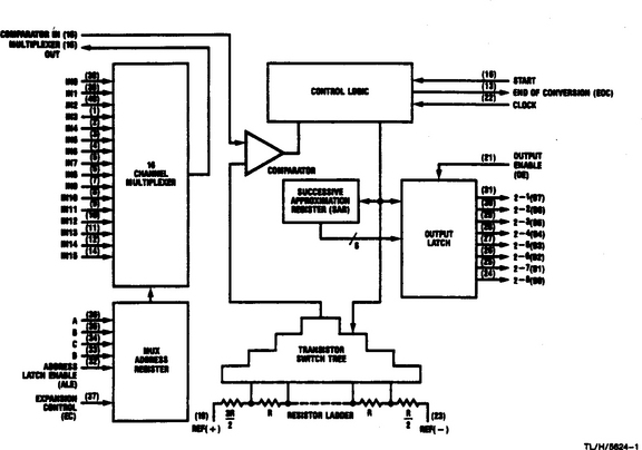
FIGURE 8-13 ADC0816/17 functional block diagram (National Semiconductor, Linear Applications Handbook, 1994, p. 590)
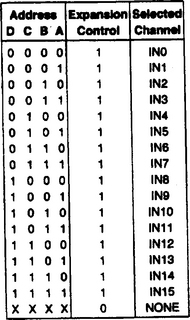
FIGURE 8-14 Analog input-selection code (National Semiconductor, Linear Applications Handbook, 1994, p. 591)
Although similar to other ADCs used in data-acquisition systems, these ICs have externally available multiplexer output and ADC-comparator input. This feature is useful when connecting signal-processing circuits to the ADC. Also, these ICs have an expansion-control pin to allow addition of more multiplexers, producing more input channels. Although the following information applies to specific ADCs, most of the principles involved can be applied to any ADC used in data-acquisition applications.
The ADC0816 is identical to the ADC0817 except for accuracy. The ADC0816 is the more accurate device, having a total unadjusted error of ±½ LSB. The ADC0817 has a total unadjusted error of ± 1 LSB (and is, as one might expect, less expensive).
8.3.1 Functional Description
As shown in Fig. 8-13, the ADCs can be divided into two major functional blocks: a multiplexer-latch and an ADC. The multiplexer-latch is composed of a 16-channel multiplexer, a 4-bit channel-select register, and some channel-select decoding circuits. The channel-select address (Fig. 8-14) is loaded on the positive transition of the address latch enable (ALE) input (Fig. 8-15). A multiplexer-enable pin called expansion control (EC) is also provided. Taking the EC pin low disables the on-chip multiplexer, allowing other multiplexers to be used, expanding the number of inputs.
The output of the multiplexer usually feeds the ADC input. The ADC is composed of the usual comparator, 256R-type resistor ladder, SAR, control logic, and output data latch. During normal operation, the ADC control logic first detects a positive-going pulse on the START input. On the rising edge of this pulse, the internal registers are cleared, and they remain clear as long as START is high. When START goes low, the conversion is initiated. The control logic cycles to the beginning of the next approximation cycle, at which time EOC (end of conversion) goes low and the actual conversion is started.
During a conversion, the control logic selects a tap on the resistor ladder, and routes the signal through a transistor switch tree to the input of the comparator. The comparator then decides whether the tap voltage is higher or lower than the input signal and indicates the decision to the control logic. The control logic then decides which tap is to be selected next.
During this process, the SAR maintains a record of the conversion sequence. As shown in Fig. 8-15, it takes 8 clock periods per approximation and requires eight approximations to convert 8 bits. Thus 64 clock periods are required for a complete conversion.
After the entire conversion is complete, the data bits in the SAR are loaded into the output register. This register requires that the outputs be enabled by the OE (output enabled) input. The data bits can then be read by the control logic.
During operation, the EOC output must be monitored to determine whether the device is actively converting or is ready to output data. When the channel address is loaded, a positive-going pulse on START starts the conversion and causes EOC to fall. When EOC goes high again, the data bits are ready to be read (by raising the OE input). The data bits can be read any time prior to one clock period before completion of the next conversion.
8.3.2 Ratiometric Conversion
Figure 8-16 shows the ADCs connected for ratiometric conversion. Because both ends of the 256R resistor ladder are available externally, the ADCs are ideally suited for use with ratiometric transducers. As discussed in Chapters 1 through 3, a ratiometric transducer is a conversion device in which the output is proportional to some arbitrary full-scale value. The actual value of the transducer output is of no great importance, but the ratio of this output to the full-scale reference is valuable. The prime advantage of a ratiometric transducer is that an accurate reference is not essential. However, the reference should be noise free, because voltage spikes during a conversion could cause inaccurate results.
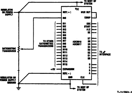
FIGURE 8-16 Ratiometric conversion with power-supply reference (National Semiconductor, Linear Applications Handbook, 1994, p. 592)
The circuit of Fig. 8-16 uses the existing 5-V supply for the reference, thus eliminating the need for a special external reference. Care should be taken to reduce power-supply noise. The supply lines should be well bypassed with filter capacitors, and it is recommended that separate PC traces be used to route the 5-V and ground to the reference inputs and to the supply pins.
8.3.3 Absolute Conversion
Figure 8-17 shows the ADCs connected for simple absolute conversion. Absolute conversion refers to the use of transducers with which the output value is not related to another voltage. The “absolute” value of the output voltage of the transducer is very important (in contrast to the output voltage of a ratiometric transducer). This implies that the reference must be accurate to determine the value of the absolute output of the transducer.
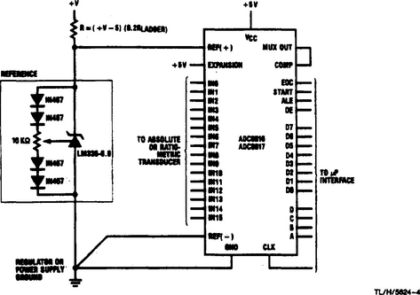
FIGURE 8-17 Simple absolute conversion (National Semiconductor, Linear Applications Handbook, 1994, p. 594)
In the circuit of Fig. 8-17, a precise, adjustable reference is provided by an LM336-5.0 and the associated parts. Ratiometric transducers also can be used in this circuit and in most of the following applications. However, the key point to remember is that accuracy of absolute conversion depends primarily on the accuracy of the reference voltage. With ratiometric systems, accuracy is determined by the transducer characteristics.
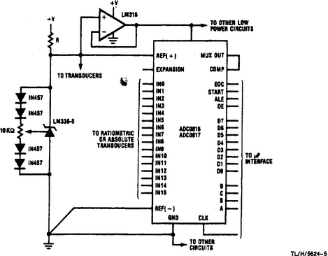
8.3.4 Using the Reference As the Supply
In some small systems (particularly CMOS) in which a reference is required, it is possible to use the reference to provide both the ADC-reference function and regulation for the supply. Figure 8-18 shows such a system in which the LM336-5.0 provides regulated 5-V for the ADC power and reference inputs, as well as for the power inputs of other component in the system. Of course, an unregulated supply greater than 5 V is required for + V.
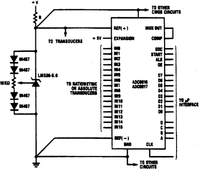
FIGURE 8-18 Reference used as a power supply (National Semiconductor, Linear Applications Handbook, 1994, p. 594)
The series resistor R is chosen such that the maximum current needed by the system is supplied, and the LM336-5.0 is kept in regulation. The value of this resistor is found with the following equation:
where VS = unregulated supply voltage; Vref = reference voltage; ILAD = Vref/1k, resistor ladder current; ITR = transducer currents, IP = system power supply requirements; and IR = minimum reference current.
Figure 8-19 shows a simple method of buffering the references to provide higher current capabilities. This eliminates the IP term in the equation for resistor R. Note that it is advisable to add some supply bypass capacitors (typically 0.1 μF) to reduce noise in the circuits of Figs. 8-18 and 8-19 (as well as Fig. 8-17). The bypass capacitors should be added to the circuits at various supply line points as necessary.
8.3.5 Eliminating Input Gain Adjustments
In some cases, it is possible to eliminate gain adjustments on the analog input signals by varying the ADC REF+ and REF– voltages to get various full-scale ranges. Figures 8-20 and 8-21 show two such circuits. In general, the reference voltage can be varied from 5 V to about 0.5 V to accommodate various input voltages. However, there is one restriction: The center of the reference voltage must be within ±0.1 V of mid-supply.
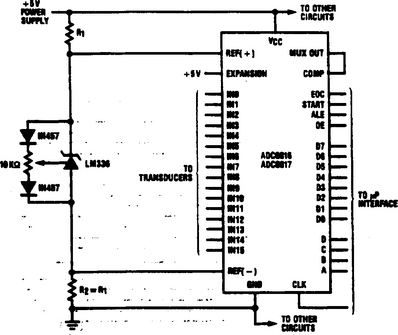
FIGURE 8-20 Supply centered reference with zener (National Semiconductor, Linear Applications Handbook, 1994, p. 595)
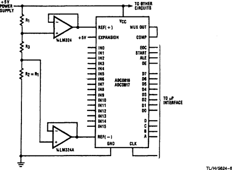
FIGURE 8-21 Supply centered reference with op amps (National Semiconductor, Linear Applications Handbook, 1994, p. 595)
The reason for this restriction is that the reference ladder is tapped by an n-channel or p-channel MOSFET switch tree (Fig. 8-13). Offsetting the voltage at the center of the switch tree from VCC/2 causes the transistors to turn off at the wrong point, resulting in inaccurate and erratic conversions. However, if properly applied, this method can reduce parts counts and eliminate extra power supplies for the input buffers.
In the supply centered reference circuit of Fig. 8-20, R1 and R2 offset REF+ and REF– from VCC and ground. An LM336-2.5 is shown, but any reference between 0.5 V and 5 V can be used.
For odd reference values, use the op-amp circuit of Fig. 8-21. Single-supply op amps such as the LM324 or LM10 can be used. R1, R2, and R3 form a resistor divider in which R1 and R3 center the reference at VCC/2, and R2 can be varied to get the proper reference magnitude.
8.3.6 Expanding Analog Input Channels
Figure 8-22 shows the ADCs connected to provide for 32-channel conversion. Such a configuration is possible because of the EC pin, which is actually a multiplexer enable. When the EC signal is low, all switches are inhibited so that another signal can be applied to the comparator input. Additional channels can be implemented as necessary.
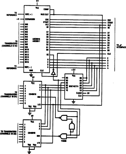
FIGURE 8-22 Simple 32-channel converter (National Semiconductor, Linear Applications Handbook, 1994, p. 596)
In the circuit of Fig. 8-22, the number of channels has been expanded from 16 to 32. A total of five address lines are required to address the 32 channels. The lower 4 bits are applied directly to the A, B, C, and D inputs. All 5 bits are also applied to an MM74C174 flip-flop that is used as an address latch for the two CD4051s. The IQ, 2Q, and 3Q outputs of the flip-flop feed the CD4051 address inputs. The 4Q and 5Q outputs are gated to form enable signals for each CD4051. Output 5Q is also applied at the EC input (after inversion) to enable the ADC multiplexer.
8.3.7 Differential Analog Inputs
Figure 8-23 shows the basic connections for implementing an ADC with differential inputs. With this circuit, the differential inputs are implemented in software. All 16 channels are paired into positive and negative inputs. Then the control logic or microprocessor converts each channel of a differential pair, loads each result, and then subtracts the two results.
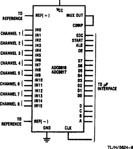
FIGURE 8-23 Basic ADC with differential inputs (National Semiconductor, Linear Applications Handbook, 1994, p. 597)
This method requires two single-ended conversions to do one differential conversion. As a result, the effective differential-conversion time is twice that of a single channel, or a little more than 200 μs (assuming a clock of 640 kHz). The differential inputs should be stable throughout both conversions to produce accurate results.
Figure 8-24 shows a differential 16-channel converter using one ADC and a few additional parts. This circuit is actually a modified version of the circuit in Fig. 8-22. The CD4051 addressing is changed, and a differential amplifier is added between the multiplexer outputs and the comparator input.
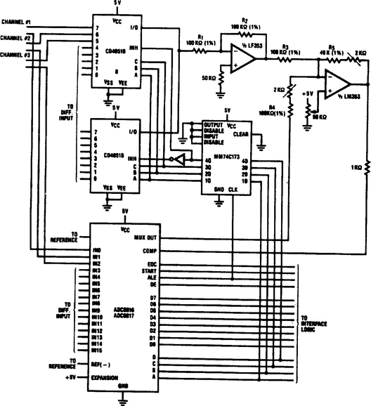
FIGURE 8-24 Differential 16-channel converter (National Semiconductor, Linear Applications Handbook, 1994, p. 598)
In the circuit of Fig. 8-24, the select logic for the CD4051s is modified to enable the switches so that they can be selected in parallel with the ADC. The outputs of the three multiplexers are connected to a differential amplifier, composed of two inverting amplifiers with gain and offset trimmers. A dual op-amp configuration of inverting amplifiers can be trimmed easily and has less stringent feedback-resistor matching requirements than a single op-amp design.
The transfer equation for the dual op amp shown is:
The propagation delay through the op amps is an important consideration. There must be sufficient time between the analog switch-selection and start-conversion to allow the analog signal at the comparator input to settle. Using the LF353 op amp shown, the delay is about 5 μs. The op-amp gain and offset controls are adjusted to provide the zero and full-scale digital-output readings for the analog-input range or span.
8.3.8 Buffering Considerations
Figures 8-25 through 8-27 show some typical buffering circuits for the ADCs. Three basic ranges of input signal levels can occur when ADCs are interfaced to the real world. These are as follows: (1) signals that exceed VCC or go below ground, (2) signals with input ranges less than VCC and ground but are different from the reference range, and (3) signals that have an input range equal to the reference range. Each of these situations requires different buffering.
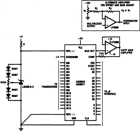
FIGURE 8-25 Single-input buffer (National Semiconductor, Linear Applications Handbook, 1994, p. 599)
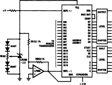
FIGURE 8-26 ±2.5-V input-range data acquisition (National Semiconductor, Linear Applications Handbook, 1994, p. 599)
FIGURE 8-27 Input-output level shifters (National Semiconductor, Linear Applications Handbook, 1994, p. 600)
In the last case (in which the signals are equal to the reference), no buffering is usually required unless the source impedance of the input signal is very high. In this case, a buffer can be added between the multiplexer output and comparator input (see Fig. 8-25). An op amp with high input impedance and low output impedance reduces input leakage (when one views the configuration from the multiplexer).
If the input signal is within the supply range but different from the reference range (or when the reference cannot be manipulated to conform to the full input range), the unity-gain buffer of Fig. 8-25 can be replaced with another op amp as shown in the inset in Fig. 8-25. This type of amplifier provides gain or offset control to produce a full-scale range equal to the reference.
When input range exceeds VCC or goes below ground, the input signals must be level-shifted before the input can go to the multiplexer. There is a limit to such level shifting when the input voltage range is within 5 V but outside the 0.5-V supply range. In this case, the supply for the entire chip can be shifted to the input range, and the digital-output signals can be level-shifted to the system 5-V supply.
A typical example of level-shifting and buffering is the situation in which the bipolar inputs range from−2.5 V to +2.5 V. If the ADCs have the supply and reference provided as shown in Fig. 8-26, then the ±2.5-V logic output can be shifted to 0-V and 5-V logic levels as shown in Fig. 8-27.
8.3.9 Digital Data Acquisition
Although the ADCs are designed for analog data acquisition, they also can be used for digital data acquisition in some cases. For example, if a system has unused channels, digital inputs can be connected to these channels instead of being separately buffered into the system. In the case of a microprocessor system, this could eliminate an I/O port and associated logic. The speed at which the inputs are accessed is one conversion cycle (which is fast enough for many applications).
The ADC inputs also can be used as input switches, power-supply indicator devices, or other system-status flags. In any configuration, the microprocessor converts the digital input channel and reads it. Software then decides whether the input is high enough (or low enough) to cause a particular action.
8.3.10 Input Considerations
Figure 8-28 shows a simplified model of the multiplexer-comparator input. As shown, the input is a sampling-type comparator in which the input current is a series of spikes, not a small DC current as might be expected. This can present a problem in some applications. The following are some points to consider.
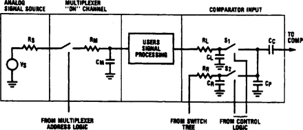
FIGURE 8-28 Simplified multiplexer-comparator input circuit (National Semiconductor, Linear Applications Handbook, 1994, p. 601)
When determining a single-bit value during a conversion, S1 closes, causing CC and CP to charge to the input voltage. Then S1 is opened and S2 is closed to sample the ladder. The resulting input current is an RC-transient charging current in which magnitude and duration depend on the values of CC, CP, RS, RM, and RL.
The duration of the transient current must be shorter than the input-sample period. In turn, the sample period depends on the converter clock frequency. As a result, the maximum source impedance (RS) depends on the clock period. As a guideline, at a clock frequency of 1 MHz the source impedance is equal to or less than 1 k. When the clock is reduced to 640 kHz, the source impedance increases to 2 k (or less). The source impedance of potentiometric transducers varies as a function of wiper position. Thus transducers with a value of 10 k (or less) are suitable for clock frequencies of 640 kHz. When the clock is increased to 1 MHz, the transducer should have a source impedance of 5 k (or less).
When a sample-and-hold or other active device (such as an op amp) is inserted between the multiplexer and comparator pins (as in Fig. 8-25), the output impedances of the transducers are no longer critical. Instead, the impedances of the sample-and-hold or op amp become the determining factor. At a clock frequency of 1 MHz, the buffer impedance should be 3 k (or less). With the clock at 640 kHz, the impedance can be 5 k (or less).
If it is not possible to avoid higher source impedances than these recommended guidelines, RC charging errors can be reduced to an average current error by placing a 1-μF capacitor from the multiplexer input to ground. Adding the capacitor averages the transient-current spikes and causes a small DC error.
For a potentiometric transducer, the DC error is:
where RP = total potentiometric resistance; IN = 2 μA (maximum input current at 640 kHz); and CK = clock frequency.
For a standard buffer source impedance, the DC error is:
where IN = 2 μA (maximum input current at 640 kHz); RS = buffer source impedance; and CK = clock frequency.
In addition to source-impedance considerations, several precautions should be observed whenever analog signals are present in a digital system. To reduce noise on the analog inputs, keep the reference input and the analog input signals physically isolated from any digital signals. As always, use a single-point ground.
8.3.11 Analog Input Overvoltage Protection
Figure 8-29 shows some protection circuits for the analog inputs. For proper operation, it is important to keep the analog input voltages to the multiplexer or comparator between VCC and ground. Of course, there might be instances in which overvoltage or undervoltage cannot be avoided. Protecting analog inputs, because of their unique nature, is usually more difficult than protecting digital inputs (which are typically on or off).
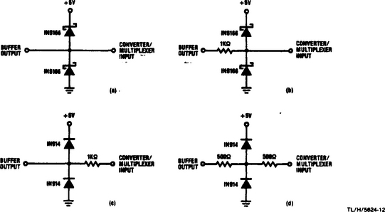
FIGURE 8-29 Protection circuits for analog inputs (National Semiconductor, Linear Applications Handbook, 1994, p. 601)
As shown in Fig. 8-29, the most effective analog-input overvoltage production circuits use some combination of Schottky diodes. Because the Schottky knee voltage is 0.4 V, the 1N5168 diodes of Fig. 8-29a safely shunt currents up to several milliamperes. For larger currents, series resistances can be added to limit current as shown in Fig. 8-29b. Do not use resistor values greater than those shown or higher than the values described in Section 8.3.10.
A less expensive solution is to replace the Schottky diodes with standard switching diodes as shown in Fig. 8-29c. However, a series resistance is required because standard diodes only partially shunt the input current (from the clamp diodes within the IC).
If the external diode must shunt a large amount of current, the two series resistors of Fig. 8-29d should be used. If the design is such that the input can exceed only one supply, the diode going to the other supply can be omitted.
8.3.12 Signal Conditioning
There are many applications in which it is desirable to add signal-processing circuits to improve converter performance. Typical additions are filter circuits, sample-and-holds, and gain-controlled amplifiers. Here again, the external accessibility of the multiplexer-output and comparator-input pins can greatly reduce the need for external circuits. This is because only one circuit is required by all 16 outputs, instead of one for each input. The following paragraphs describe some typical signal-conditioning applications.
8.3.13 Microprocessor-Controlled Gain
Figure 8-30 shows the ADCs connected for an external gain-control under supervision of a microprocessor. The CD4051 analog multiplexer is placed in the feedback loop of a simple non-inverting op amp. One controls the gain of this op amp by selecting one of the CD4051 analog switches. This switches a resistor in and out of the feedback loop. If the resistors R2N are of different value, different gains are realized. The gains are given by: Gain (AV) = 1 + (R2N/R1). A microprocessor (or some control logic) selects a gain by latching the channel address into an MM74C173.
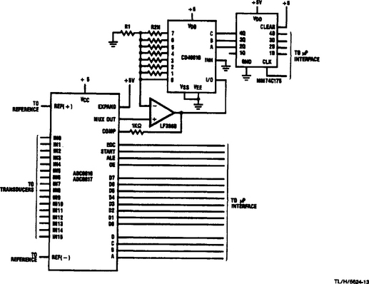
FIGURE 8-30 ADC with microprocessor-controlled gain (National Semiconductor, Linear Applications Handbook, 1994, p. 602)
It is important that the LF356B output not exceed the power supply, so, before a new channel is selected, the op-amp gain must be reduced to a new level. The 1-k resistor at the LF356B output helps protect the comparator inputs from accidental overvoltage (or undervoltage). The two back-biased diodes at the input to VCC and ground (1N914 or Schottky) offer further protection.
8.3.14 Sample-and-Hold
Figures 8-31 and 8-32 show the ADCs connected for sample-and-hold (S/H) operation. The S/H function is the only major data-acquisition element not included in these ADCs. If the input signals are fast moving, then an S/H should be used to quickly acquire the signal and then hold the signal while the ADCs convert it to a digital readout. This can be easily implemented by means of insertion of the S/H between the multiplexer output and the comparator input as shown.
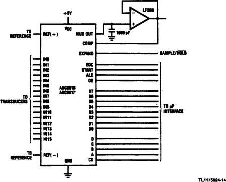
FIGURE 8-31 Sample-and-hold with op amp (National Semiconductor, Linear Applications Handbook, 1994, p. 603)
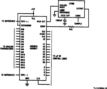
FIGURE 8-32 Sample-and-hold with IC S/H (National Semiconductor, Linear Applications Handbook, 1994, p. 604)
In the simplest form, the multiplexer output is connected to the comparator input, with a capacitor connected to ground (similar to that shown in Fig. 8-31 but without the op amp). The expansion-control pin is used as a sample-control input. When EXPAND is high, one switch is on and the capacitor voltage follows the input. When EXPAND is low, all switches are turned off and the capacitor holds the last value.
Unfortunately, this simple solution is not practical. The input bias to the comparator is about 2 μA (worst case, with a clock of 640 kHz). The droop or discharge rate for a 1000-pF capacitor is about 2000 V/s or about 0.2-V per conversion. This is not practical. If a 0.01-μF capacitor is used instead, the rate is about 20 μV, which might work. However, the acquisition time would be about 100 μs, or about the length of a conversion.
The circuit of Fig. 8-31 eliminates the problem produced by the high comparator-input leakage. With the LF356 buffer connected between the multiplexer-output and comparator-input pins, the leakage is reduced from 2 μA to about 100 nA. The droop-per-conversion is typically less than 1.0 μV per conversion (with a 1000 pF capacitor) and the acquisition time is about 20 μs (instead of the 100 μs).
The circuit of Fig. 8-32 isolates the capacitor from both the multiplexer and comparator pins using an LF398 IC S/H. Acquisition time for the LF398 is a typical 4 μs (to 0.1%), and the droop rate is about 20 μV/conversion. Because the LF398 has its own S/H input, the expansion control of the ADC is free to be used in the normal manner.
No matter what configuration is used, the choice of the hold capacitor is critical to the performance of the S/H circuit. Some capacitors are composed of dielectrics that have an initial droop after the hold function is strobed. This is because of dielectric absorption. Polypropylene and polystyrene dielectrics have very little dielectric absorption and thus make good S/H capacitors. Materials such as Mylar polyethylene have higher absorption properties and should not be used for S/H circuits.
8.3.15 Filtering Analog Inputs
Filtering might be required for some analog-input signals, especially signals from a noisy environment. High-frequency noise is a particular problem. The ADCs can accommodate the addition of most standard low-pass filters. Another useful filter is a 50-Hz or 60-Hz notch filter to eliminate the noise contributed to the circuit by AC power lines.
A single passive filter can be placed between the multiplexer-output and comparator-input pins. However, such passive filters must be carefully designed to reduce input loading. The filter capacitor tends to average the comparator sampling current. To eliminate this effect, use an op amp to buffer the filter, or use an active filter. If you are not familiar with filter-circuit design, read McGraw-Hill Circuit Encyclopedia & Troubleshooting Guide volumes 1, 2, and 3 (McGraw-Hill, 1996).
8.3.16 Microprocessor Interface Considerations
Figures 8-33 and 8-34 are flow charts for interrupt-control and polled-I/O modes of microprocessor interface, respectively. Either interface can be used, but the polled-I/O method usually requires fewer external components. With polled-I/O, the microprocessor or CPU periodically interrogates the ADC, which looks like an I/O port to the CPU. With interrupt-control, the ADC appears as a memory and interrupts the CPU. From a simplified-design standpoint, the major concern is whether the EOC (Fig. 8-15) should be polled by the microprocessor or should cause an interrupt. The remainder of this section describes both approaches.
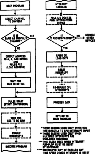
FIGURE 8-33 Flow chart for interrupt control (National Semiconductor, Linear Applications Handbook, 1994, p. 605)
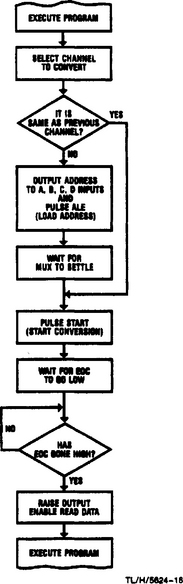
FIGURE 8-34 Flow chart for polled-I/O (National Semiconductor, Linear Applications Handbook, 1994, p. 605)
Even though the actual timing of CPU read and write cycles varies, most microprocessors output the address and data (during write) onto the system buses. A certain time later, the read or write strobes go active for a specified time. The interface logic must detect the state of the address and data buses and initiate the action. For the ADCs in this chapter, these actions are: (1) load channel address, (2) start conversion, (3) detect EOC, and (4) read the resultant data. One performs these actions by decoding the read-write strobes, address, and data to form ALE and START pulses, then to detect EOC, and finally to read the data.
Typical decoding and strobe generation are straightforward. The START, ALE, and OUTPUT ENABLE strobes generally are of the same duration as the CPU read-write strobes and are positive-going (although ALE can be negative-going). One possible concern is where to take the A, B, C, and D channel-select address. These lines can be connected to either the address bus or the data bus. The advantage of using the data bus is that in minimum systems, more I/O address lines are available for simple decoding. When the A, B, C, and D inputs are connected to the address bus, each analog channel becomes a separate I/O port.
It is possible to connected the START and ALE pins together so that one pulse can both write the channel address and start the conversion. However, it is essential that the comparator-input signal be stable before conversion starts. If not, the first (and most important) successive approximation could be in error. Typical START and ALE pulses are the same length as the CPU read and write strobes (normally 0.2- to 1-μs long). As a result, conversion can start within 1 μs of the address-select latching. (As shown in Fig. 8-15, the channel is selected on the rising edge of ALE, and conversion begins within eight clock periods of the falling edge of START.)
When clock speed is greater than 500 kHz, 1 μs might not be enough time to allow the analog input signal to pass through the multiplexer and any additional signal-conditioning circuits such as buffers and S/H. However, there are two relatively simple ways to overcome this problem. First, the START/ALE pulse can be stretched to the desired length with a one-shot (such as an MM74C221). This produces a pulse as long as the total delay from multiplexer input to comparator input. As an alternative, the converter can be “double pulsed” in software by writing to the START/ALE address twice. The first pulse latches the desired channel address and starts the conversion. The second pulse must again load the same channel address, which does not change the multiplexer state, and then restarts the conversion. The second pulse must occur after the comparator input has settled.
8.3.17 Interfacing 8080-Type Microprocessors
Figures 8-35 and 8-36 show connections for interface to 8080-type microprocessors (INS8080/8224/8228). This interfacing is quite simple because the INS8080 CPU has separate I/O read (I/OR) and I/O write (I/OW) strobes (or separate I/O addressing). As a result, in these simple interface systems, little or no address decoding is required.
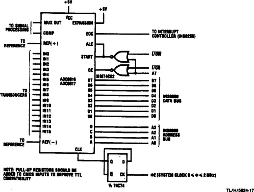
FIGURE 8-35 Simple 8080 interface (National Semiconductor, Linear Applications Handbook, 1994, p. 606)
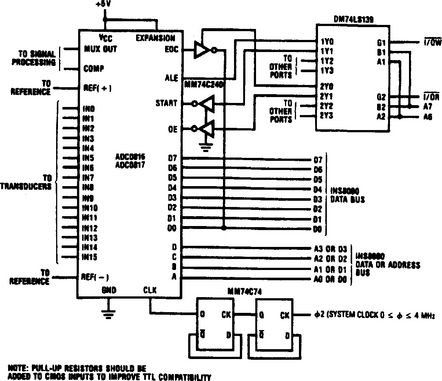
FIGURE 8-36 8080 interface with partial decoding (National Semiconductor, Linear Applications Handbook, 1994, p. 607)
As shown in Fig. 8-35, two NOR gates are used to gate the I/O strobes with the most-significant address bit A7. (The INS8080 has 8 bits of port address, yielding a maximum of four I/O ports if inputs A, B, C, and D are connected to the address bus.) An MM74C74 flip-flop is used as a divide-by-2 to generate a converter clock of 1 MHz. If the system clock is equal to or less than 1 MHz, the flip-flop can be omitted.
Typical software for the Fig. 8-35 circuit first writes the channel address to the converter as a start signal. Two start pulses are sent to the ADCs to allow the comparator input to settle. After the second start pulse, the CPU can execute other program segments until the CPU is interrupted by EOC going high. Depending on interrupt structure, program control then is given to the interrupt handler, which reads the converter data.
The circuit of Fig. 8-36 uses a DM74LS139 dual 2-4 decoder in which one-half of the chip is used to create read pulses, and the other half to create write pulses. The START and OE inputs are inverted to provide the correct pulse polarity. This interface partially decodes A6 and A7 to provide more I/O capabilities than the Fig. 8-35 circuit. The Fig. 8-36 circuit also implements a simple polled-I/O structure. The EOC output is placed on the data bus by a tristate inverter when the inverter is enabled by a read pulse from the INS8080.
8.3.18 Interfacing Z80-type Microprocessors
Figures 8-37 and 8-38 show connections for interface to Z80-type microprocessors. The Z80, even though architecturally similar to the INS8080, uses slightly different control lines to perform I/O reads and writes. In Fig. 8-37, NOR gates are used to strobe the I/O functions. However, the Z80 has RD (read) and WR (write) strobes, which are gated with IOREQ (I/O request).
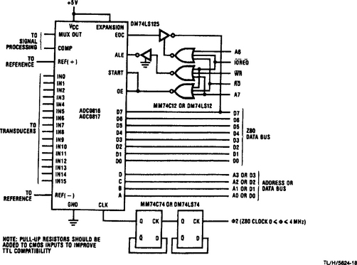
FIGURE 8-37 Simple Z80 interface (National Semiconductor, Linear Applications Handbook, 1994, p. 607)
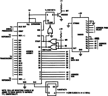
FIGURE 8-38 Decoded Z80 interface (National Semiconductor, Linear Applications Handbook, 1994, p. 608)
In the circuit of Fig. 8-37, START is connected to OE. This causes a new conversion to be started whenever the data bits are read. This might seem unusual, but it can be useful if the converter is to be continually restarted on completion of the previous conversion. Address bit A6 is used to drive a strobe that places EOC on the data bus to be read by the CPU.
In the circuit of Fig. 8-38, a 6-bit comparator is used to decode A4-A7 and IOREQ. Two NOR gates are used to gate the ALE/START and OE pulses. This design functions the same as that of Fig. 8-37, except that the DM8131 provides much more decoding.
8.3.19 Interfacing NSC800 Microprocessors
Figures 8-39 and 8-40 show connections for interface to NSC800 microprocessors. This interface is quite similar to that for the 8080, even though the timing is very different. The NSC800 multiplexes the lower 8 address bits on the data bus at the beginning of each cycle. When accessing memory, A0-A7 must be latched out at the beginning of a read or write cycle.
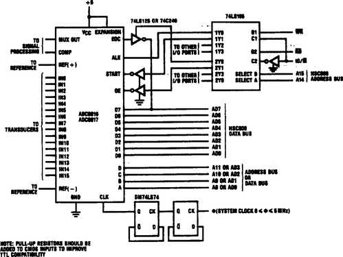
FIGURE 8-39 Partially decoded NSC800 interface (National Semiconductor, Linear Applications Handbook, 1994, p. 608)
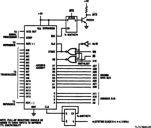
FIGURE 8-40 Minimum NAC800 interface (National Semiconductor, Linear Applications Handbook, 1994, p. 609)
For I/O accessing, the NSC800 duplicates the 8-bit I/O addresses on A8-A15 address lines. Latches are not necessary because these lines are not multiplexed. The I/O read and write strobes are taken from RD (read) and WR (write) lines and the IO/M signal.
The circuit of Fig. 8-39 uses a dual 2-4 line decoder that decodes A15. A14 is enabled by the read-write strobes. Tristate inverters are used to implement a decoding similar to that of Fig. 8-36. Double pulsing is not required because START and ALE are accessed separately.
The circuit of Fig. 8-40 uses NOR gates (similar to that of Fig. 8-35) but with different control signals. When EOC goes high, the flip-flop is set, and INTR goes low. When the NSC800 acknowledges the interrupt by lowering INTA, the flip-flop resets. If more than one interrupt can occur simultaneously, either INTA should be gated with EOC, or a signal other than INTA must be used. This is required because the NSC800 can detect another interrupt and clear the ADC interrupt before the ADC signal is detected.
8.3.20 Interfacing 6800-type Microprocessors
Figures 8-41 and 8-42 show connections for interface to classic 6800 microprocessors. Because the 6800 has no separate I/O addressing capabilities, the system I/O must be addressed as though it is memory. As discussed, memory mapping can require more address decoding to separate memory for I/O. In small systems, however, the parts count can still be kept to a minimum.
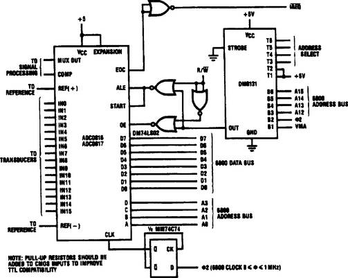
FIGURE 8-41 Simple 6800 interface (National Semiconductor, Linear Applications Handbook, 1994, p. 610)
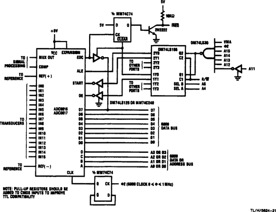
FIGURE 8-42 Partially decoded 6800 interface (National Semiconductor, Linear Applications Handbook, 1994, p. 610)
Figure 8-41 shows an interface in which a DM8131 comparator is used to partially decode the A12, A13, A14, and A15 address lines with the 2 clock and VMA (valid memory address). This provides an address decode pulse for the two NOR gates, which in turn generate the START/ALE pulse and the output-enable OE signal. The design locates the ADC in one 4-k byte or block.
The circuit of Fig. 8-41 ties EOC to IREQ interrupt through an inverter, and is usable only in single-interrupt systems because the 6800 has no way of resetting the interrupt (except by starting a new conversion). Because EOC is directly tied to the interrupt input, the controlling software must not re-enable interrupts until eight converter clock periods after the START pulse, when EOC is low.
Figure 8-42 shows an interface with more I/O port strobes. A NAND gate and inverter are used to decode the addresses, VMA, and 2 clock. The I/O addresses are located at 11110XXXXXAABBBB (binary); where X = don’t care; A = 00 (binary) for ALE write or IREQ reset/EOC read and A = 01 for START write or data read; and B = channel-select address, if A, B, C, and D are connected to the address bus and ALE is accessed. A dual 2-4 line decoder is used to generate these strobes. Inverters are used to create the correct logic levels.
The 6800 supports only a wired-OR interrupt structure. In a multi-interrupt environment, only one interrupt is received and the interrupt-handler routine must determine which device has caused the interrupt and must service that device. To do this, the EOC is brought out to the data bus so that EOC can be checked by the CPU.
8.3.21 Parallel Interface
In some cases, microprocessor-support ICs can be used to interface the ADCs to microprocessors. Most parallel I/O chips can be used, and they provide enough flexibility for all functions to be under software control.
The manufacturer recommends INS8255, 6820, and Z80s-PI0 (or some similar device) for parallel I/O. In most cases, these support ICs can be connected directly to the data and control pins. Software is then used to manipulate the START and ALE pins via the interface chip. In some cases, the chips provide handshaking or interrupt capabilities and possibly a clock. If not, such functions must be provided by other circuits. Keep in mind that parallel I/O circuits are usually more expensive than the circuits they replace, although such support ICs can simplify design and increase versatility.
8.4 Circuit Applications with Multiplying DACs
Figure 8-43 shows the internal functions of a multiplying DAC. Because such four-quadrant DACs allow a digital word to operate on an analog input, or vice versa, the output can represent a sophisticated function. CMOS multiplying DACs allow true bipolar analog signals to be applied to the reference input. This feature makes such DACs useful in many applications not generally considered data converters. The following paragraphs describe some typical applications for multiplying DACs.
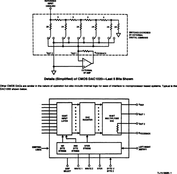
FIGURE 8-43 Internal functions of a multiplying DAC (National Semiconductor, Linear Applications Handbook, 1994, p. 659)
8.4.1 Sine-Wave Generator with Digital Control
Figure 8-44 shows a variable-frequency sine-wave generator capable of producing signals at frequencies up to 30 kHz under digital control. This function is valuable in automatic test equipment and instrumentation applications and is not easily achieved in normal sine-wave generation circuits. The linearity of output frequency to digital-code input is within 0.1% for each of the 1,024 discrete output frequencies.
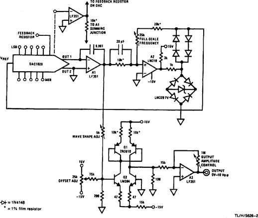
FIGURE 8-44 Sine-wave generator with digital control (National Semiconductor, Linear Applications Handbook, 1994, p. 660)
To understand circuit operation, assume that the A2 output is negative. This means that the zener-determined output of A2 applies −7 V to the DAC reference input. Under these conditions, the DAC pulls a current from the A1 summing junction. The current is directly proportional to the digital code applied to the DAC. Integrator A1 ramps far enough so that the potential at the A2 +input just goes positive. The A2 output changes state, and the potential at the DAC reference input changes to +7 V. The DAC output current reverses and the A1 integrator is forced to move in the negative direction. When the negative-going output of A1 becomes large enough to pull the A2 + input slightly negative, the A2 output changes state and the process repeats.
The amplitude-stabilized triangle wave at the A1 output has a frequency that depends on the digital word at the DAC. The 20-pF capacitor provides a slight leading response at high frequencies to offset the 80-ns response time of A2. This aids overall circuit linearity. The triangle wave is applied to the Q1/Q2 shaper network, which provides a sine-wave output.
To adjust the circuit, set all DAC digital inputs high and trim the 25-k pot for 30-kHz output (using a frequency counter). Then connect a distortion analyzer to the circuit output and adjust the 5-k and 75-k pots for minimum distortion. Finally, set the 1-M output control for the desired output.
This circuit provides rapid switching of output frequency, as shown in Fig. 8-45. Note that the output frequency shifts immediately (actually with no undesired delay) by more than an order of magnitude in response to digital commands (top line of Fig. 8-45).
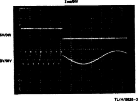
FIGURE 8-45 Sine-wave generator oscilloscope display (National Semiconductor, Linear Applications Handbook, 1994, p. 660)
If operation over temperature is required, the absolute change in resistance in the DAC internal ladder might cause unacceptable errors. This can be corrected by reversing the A2 inputs and inserting an amplifier (dashed lines in Fig. 8-44) between the DAC and A1. Because this amplifier uses the DAC internal feedback resistor (Fig. 8-43), the temperature error in the ladder is cancelled. This results in more stable operation.
8.4.2 Digitally Programmable Pulse-Width Modulation
Figure 8-46 shows the DAC used to program the pulse width of clock signals under digital control. This function is valuable in automatic testing of secondary-breakdown limits for switching transistors. However, the high resolution of control that the circuit has over the pulse width is useful anywhere wide range, precision, pulse-width modulation (PWM) is required.
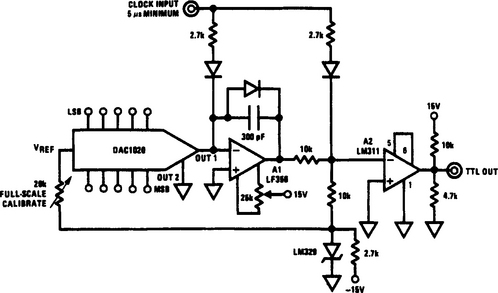
FIGURE 8-46 Digitally programmable pulse-width modulator (National Semiconductor, Linear Applications Handbook, 1994, p. 661)
In this circuit, the length of time required by the A1 integrator to charge to a reference level is determined by the current from the DAC. In turn, the current is directly proportional to the digital code at the DAC input. Both the DAC analog input and the reference trip point are taken from the LM329 voltage reference.
While the integrator output (trace A of Fig. 8-47) is below the trip point, A2 comparator output remains high (trace B). When the trip point is exceeded, A2 output goes low. The DAC input code can vary the output pulse width over a range determined by the DAC resolution.
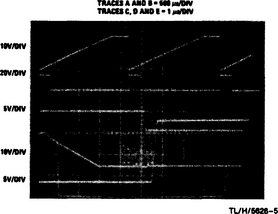
FIGURE 8-47 Pulse-width modulator oscilloscope display (National Semiconductor, Linear Applications Handbook, 1994, p. 661)
Traces C, D, and E of Fig. 8-47 show the fine detail of the resetting sequence. (The horizontal scale is expanded for these traces.) Trace C is the 5-μs clock pulse. When this pulse rises, the A1 integrator output (trace D) is forced negative until the output reaches the limit of the diode in the feedback loop. While the clock pulse is high, current through the 2.7-k diode path forces the A2 output low. When the clock pulse goes low, the A2 output goes high and remains high until the A1 integrator output-amplitude exceeds the trip point.
To calibrate this circuit, set all DAC bits high, and adjust the FULL-SCALE CALIBRATE pot for the desired full-scale pulse width. Then set only the DAC LSB high, and adjust the A1 offset pot for the appropriate length. (This is 1/1024 of the full-scale value for a 10-bit DAC.) If the 2.2-mV/°C drift of the clamp diode in the A1 feedback loop is objectionable, replace the diode with an FET switch.
8.4.3 Log Amplifier with Digitally Controlled Scale Factor
Figure 8-48 shows the DAC used to program the scale factor of a logarithmic amplifier under digital control. Log amplifiers are commonly used in applications that require a wide dynamic-measurement range (such as in photometry), and it is often necessary to set the amplifier scale factor for some given value.
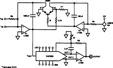
FIGURE 8-48 Log amplifier with digitally controlled scale factor (National Semiconductor, Linear Applications Handbook, 1994, p. 662)
In this circuit, Q1 is the actual log-converter transistor. Q2 and the 1-k resistor provide temperature compensation. The log-amplifier output is taken at A3. The digital code applied to the DAC determines the overall scale factor of the input-voltage (or current) to output-voltage ratio.
8.4.4 Amplifier with Digitally Controlled Gain
Figure 8-49 shows the DAC used to program the gain of an amplifier under digital control. The amplifier handles bipolar input signals. In this circuit, the input is applied to the amplifier through the DAC feedback resistor. The digital code selected at the DAC determines the ratio between the DAC feedback resistor and the impedance that the DAC ladder presents to the op-amp feedback path.
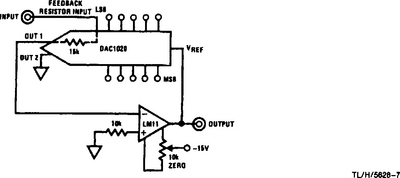
FIGURE 8-49 Amplifier with digitally controlled gain (National Semiconductor, Linear Applications Handbook, 1994, p. 662)
If no digital code (all 0s) is applied to the DAC, there will be no feedback and the amplifier will saturate. If this condition is objectionable, a large-value (22-M) resistor can be shunted across the DAC feedback path. This has little effect at lower frequencies. The gain accuracy of this circuit depends directly on the open-loop gain of the amplifier, not on the DAC.
8.4.5 Digitally Controlled Filter
Figure 8-50 shows the DAC used to program the cutoff frequency of a filter. (The equation given in the figure governs the cutoff frequency.) In this circuit, the DAC provides high-resolution digital control of frequency response by effectively varying the time constant of the A3 integrator. This is shown in Fig. 8-51 (which is a scope presentation of the test circuit in Fig. 8-50).
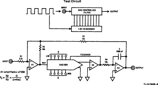
FIGURE 8-50 Digitally controlled filter (National Semiconductor, Linear Applications Handbook, 1994, p. 663)
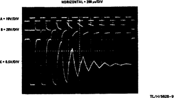
FIGURE 8-51 Digitally controlled filter oscilloscope displays (National Semiconductor, Linear Applications Handbook, 1994, p. 663)
When each input square wave is presented to the filter, the 1-of-10 decoder shifts a 1 to the next DAC digital-input line, in sequence. Trace A is the input waveform, and trace B is the waveform at the A1 output (which is the reference input of the DAC). The circuit output at A3 appears at trace C. When the circuit shifts the 1 toward the lower-order DAC inputs, the cutoff frequency decays rapidly (as shown in trace C).
8.5 Some Classic CMOS DAC Applications
This section is devoted to some classic applications for CMOS DACs. Although the circuits show the National Semiconductor MICRO-DAC™ devices, the circuits can be adapted to other DACs, provided that the DACs have similar characteristics and features (such as an internal feedback resistor), and are CMOS. MICRO-DAC™ is a registered trademark of National Semiconductor Corporation.
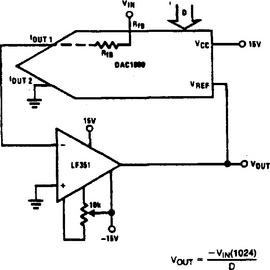
8.5.1 Digital Potentiometer
Figure 8-52 shows the basic connections for a DAC operated as a digital potentiometer. In this circuit, the applied digital-input word multiplies the applied reference voltage. The resultant output voltage is the product of this multiplication, normalized to the resolution of the DAC. The op amp converts the DAC output current to a voltage through the 15-k feedback resistor within the DAC.
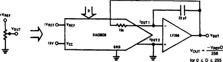
FIGURE 8-52 Digital potentiometer (National Semiconductor, Linear Applications Handbook, 1994, p. 665)
In this particular DAC, the output current ranges from a near-zero output leakage (about 15 nA) for an applied code of all Os (D = 0), to a full-scale value (D = 2n–1); where D = decimal equivalent of the binary input, and n = the bits of resolution of the DAC, of Vref divided by the R value of the internal R-2R ladder network (nominally 15 k). The current at IOUT 2 is equal to that caused by the one’s-complement of the applied digital input (with IOUT 1 at full-scale, IOUT 2 is zero).
The output voltage is the opposite polarity of the applied reference voltage. However, because the DAC is CMOS, bipolar reference voltages can be used. For example, if a positive output is needed, a negative reference can be applied.
To preserve output linearity, the two current-output pins must be as close to 0 V as possible. This requires that the input-offset voltage of the op amp be nulled. The amount of linearity-error degradation is about Vos + Vref. When the digital pot is used to attenuate AC signals (in audio applications for example), the DAC linearity over the full range of the applied reference voltage (even if it passes through zero) is good enough to distort a 10-V sine wave by only 0.004%.
The feedback capacitor shown in Fig. 8-52 is added to improve the settling time of the output when the input code is changed. Without this compensation, there can be ringing and overshoot in the output (because of the usual feedback-pole caused by the feedback resistor and the DAC output capacitance).
As usual, the op amp should have good DC characteristics (low offset voltage (VOS) and low VOS drift) as well as fast AC characteristics (high slew rate, short settling time, and wide bandwidth). If any of these terms is unfamiliar, read my Simplified Design of IC Amplifiers (Newnes, 1996).
If it is not practical to find an op amp that meets all these requirements, it is possible to use a combination of op amps such as shown in Fig. 8-53. This circuit combines the excellent DC input characteristics of the classic LM11 with the fast response of an LF351 (a combination bipolar device).
8.5.2 Level-Shifting the Output Range
Figure 8-54 shows the basic connections for a DAC operated to shift the output level. The shift is made by summing a fixed current to the DAC current-output terminal, offsetting the output voltage to the op amp. The applied referenced voltage then serves as the output-span controller and is added (in fractions) to the output as a function of the applied digital code.
8.5.3 Single-Supply Operation
Figure 8-55 shows the DAC connected for single-supply operation. The R-2R ladder can be operated as a voltage-switching network to circumvent the output-voltage inversion inherent in the current-switching mode. In this circuit, the reference voltage is applied to the IOUT 1 terminal and is attenuated by the R-2R ladder in proportion to the applied code. The voltage is then output to the Vref terminal with no phase inversion.
FIGURE 8-55 DAC connected for single-supply operation (National Semiconductor, Linear Applications Handbook, 1994, p. 666)
To ensure linear operation in this mode, the applied reference voltage must be kept less than 3 V for 10-bit DACs, or less than 5 V for 8-bit DACs. The supply voltage to the DAC must be at least 10 V more positive than the reference voltage to ensure that the CMOS ladder switches have enough voltage overdrive to fully turn on. An external op amp can be added to provide gain to the DAC output voltage for a wide overall output span.
The zero-code output voltage is limited by the low-level output-saturation voltage of the op amp. The 2-k load resistor helps to minimize the voltage. This circuit provides generally good linearity for 8-bit and 10-bit DACs but can have a linearity problem with 12-bit DACs (because of the very low reference required). DACs designed specifically for single-supply operation (including 12-bit DACs) are described in this chapter. Such DACs should be used if single-supply operation is essential.
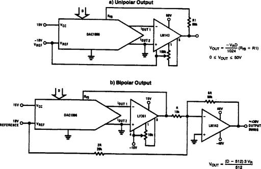
8.5.4 Bipolar Output from a Fixed Reference Voltage
Figure 8-56 shows the DAC connected to provide a bipolar output from a fixed reference voltage. This connection is made with a second op amp in the analog-output circuit. In effect, the circuit gives sign significance to the MSB of the digital-input word, allowing four-quadrant multiplication of the reference voltage. The polarity of the reference can still be reversed (or can be an AC signal) to realize full four-quadrant multiplication.
8.5.5 DAC-Controlled Amplifier
Figure 8-57 shows the basic connections for DAC control of an amplifier. In this circuit, the DAC is used as the feedback element for an inverting-amplifier configuration. The R-2R ladder digitally adjusts the amount of output signal fed back to the amplifier summing junction. The feedback resistance can be thought of as varying from about 15 k to infinity when the input code changes from full scale to zero. The internal feedback resistor is used as the amplifier input resistor. When the input code is all 0s, the feedback loop is opened and the op-amp output saturates.
8.5.6 Capacitance Multiplier
Figure 8-58 shows the basic connections for capacitance multiplication. Actually, the circuit is a DAC-controlled amplifier (used for capacitance multiplication) to give a microprocessor control of system time-domain or frequency-domain response. In simple terms, the microprocessor controls the digital input to the DAC, which controls the amplifier to produce a variable capacitance. The capacitance can be used to vary the time constant of RC circuits, varying either time or frequency.
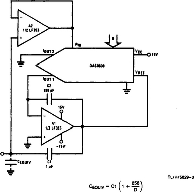
FIGURE 8-58 Capacitance multiplier (National Semiconductor, Linear Applications Handbook, 1994, p. 667)
In this circuit, the DAC adjusts the gain of a stage with fixed capacitive feedback. This produces a Miller-effect equivalent input capacitance equal to the fixed capacitance multiplied by 1 plus the amplifier gain. The voltage across the equivalent input capacitance to ground is limited to the maximum output voltage of op amp A1, divided by 1 plus 2n/D; where n = the DAC bits of resolution, and D = decimal equivalent of the binary input.
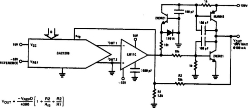
8.5.7 High-Voltage Output
Figure 8-59 shows how higher output voltages can be obtained from a DAC (both unipolar and bipolar outputs). The output current of these circuits depends on the current limit of the LM143 op amp (typically 20 mA). Figure 8-60 shows how a discrete power stage can be added to further increase output current capability (to 100 mA at 100 V).
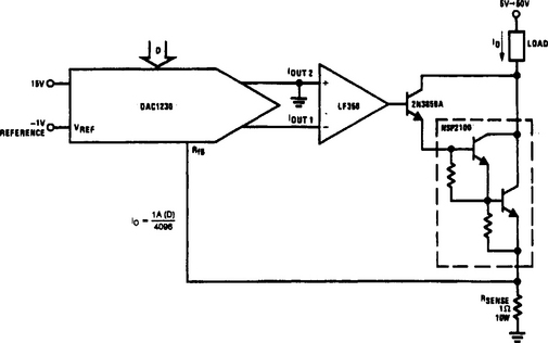
8.5.8 High-Current Controller
Figure 8-61 shows a DAC used to provide digital control of a 1-A current sink. Such a circuit can be used for heater control, stepper-motor torque compensation, and automatic test equipment. The largest source of nonlinearity in this circuit is the stability of the current-sensing resistance (with changes in power dissipation). The sensing resistance should be kept as low as possible to minimize this effect. The reference voltage must be reduced (to−1 V, as shown) to maintain the output-current range. The triple Darlington is used to minimize the base-current flowing through the sensing resistance, while simultaneously maintaining the collector current flow to the load.
8.5.9 Current-Loop Controller
Figure 8-62 shows a DAC used to provide digital control of the standard 4-mA to 20-mA industrial-process current loop. The circuit is two-terminal, and all circuit components (including the DAC) are powered directly from the loop.
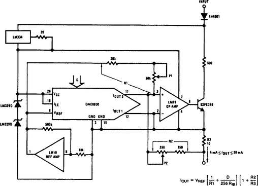
FIGURE 8-62 Current-loop controller (National Semiconductor, Linear Applications Handbook, 1994, p. 670)
In this circuit, the output transistor conducts whatever current is necessary to keep the voltage across R3 equal to the voltage across R2. This voltage, and therefore the total loop current, is directly proportional to the output current from the DAC. The net resistance of R1 is used to set the zero-code loop current to 4 mA, and R2 is adjusted to provide the 16-mA output span for a full-scale DAC code. The entire circuit floats by operating at whatever ground-reference potential is required for the total loop resistance and loop current.
To ensure proper operation, the voltage differential between the input and output terminals must be kept in the range of 16 V to 55 V, and the digital inputs to the DAC must be electrically isolated from the ground potential of the controlling microprocessor. This isolation can best be achieved with opto-isolators.
In a non-microprocessor-based system in which the loop-controlling information comes from thumbwheel switches (or a similar mechanical device), the digital input for the DAC can be taken from BCD-to-binary CMOS logic circuits (which are ground referenced to the ground potential of the DAC). The total supply current requirements of all circuits used must (of course) be less than 4 mA, and R1 can be adjusted accordingly.
8.5.10 Tare Compensation
Figure 8-63 shows a DAC (and an ADC) used to provide digital tare compensation. Such a function is used in a weighing system in which the weight of the scale platform, and possibly a container, is subtracted automatically from the total weight being measured. In effect, this expands the range of weight that can be measured by preventing a premature full-scale reading and allows an automatic indication of the actual unknown quantity.
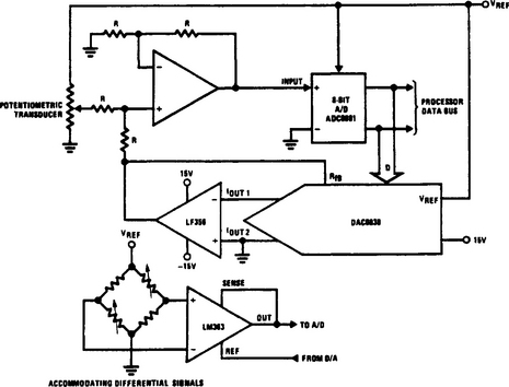
FIGURE 8-63 Basic tare compensation (National Semiconductor, Linear Applications Handbook, 1994, p. 670)
In the basic system of Fig. 8-63, the DAC is initially given a zero code, and the system input is set to a reference quantity. A conversion of the input is performed, then the corresponding code is applied to the DAC. The DAC output then is equal to and of opposite polarity to the input voltage. This forces the amplifier output, and the ADC input, to zero. (In this case, an 8-bit ADC is used.)
The DAC output is held constant so that any subsequent ADC conversion will yield a value relative in magnitude to the initial reference quantity. To ensure that the output code from the ADC generates the correct DAC output voltage, the two devices should be driven from the same reference voltage. For differential input signals, an instrumentation amplifier (such as an LM363) can be used. The output reference pin of the LM363 can be driven directly by the DAC as shown. This will offset the ADC input.