
Data Converter Basics
This chapter is devoted to basic data converters, both analog-to-digital and digital-to-analog. The chapter is primarily for readers who are totally unfamiliar with data converters. It is possible to design data-converter circuits from scratch. However, data converters are available in integrated circuit (IC) form, and it is generally simpler to use such ICs.
The data sheets for IC converters often show the connections and provide all necessary design parameters to produce complete converter circuits by adding external components. This chapter describes the function and operation of IC converters to help you understand the data sheet information.
Before we get started, let us resolve certain differences in terms. Some manufacturers refer to analog-to-digital converters as ADCs. Other manufactures use the term A/D converter. The same is true of digital-to-analog converters, which are referred to as DACs by some, and as D/A converters by others. I prefer the terms ADC and DAC, but do not be surprised to find both terms in this book.
1.1 Basic Data Conversion Techniques
This section describes the various ADC and DAC techniques in common use. Here we concentrate on explanations of the basic principles of data conversion. By studying this information, you should be able to understand operation of the converter IC described throughout the book. It is assumed that you are familiar with basic digital electronics. If not, read Lenk’s Digital Handbook (McGraw-Hill, 1993).
1.1.1 Typical BCD Signal Formats Used in ADC/DAC Circuits
Figure 1-1a shows the relationship of the three most common BCD (binary coded decimal) signal formats: NRZL (nonreturn-to-zero level), NRZM (nonreturn-to-zero-mark), and RZ (return-to-zero).

In NRZL, a 1 is one signal level, and a 0 is another signal level. These levels can be 5 V, 10 V, 0 V, −5 V, or any other selected values, provided that the 1 and 0 levels are entirely different.
In RZ, a 1-bit is represented by a pulse of definite width (usually a ½-bit width) that returns to zero signal level, and the 0-bit is represented by a zero-level signal.
In NRZM, the level of the pulse has no meaning. A 1 is represented by a change in level, and a 0 is represented by no change.
1.1.2 Four-Bit System in the Conversion Process
Figure 1-1b shows the relation between two voltage levels to be converted, and the corresponding binary code (in NRZL form), in a basic ADC. In practice, a four-bit ADC (sometimes called a binary encoder) samples the voltage level to be converted and compares the voltage to ½ scale, ¼ scale, 1/8 scale, and 1/16 scale (in that order) of a given full-scale voltage. The ADC then produces four data bits, in sequence, with the comparison made on the most significant (½ scale) first.
As shown in Fig. 1-1b, each of the two voltage levels is divided into four equal time increments. The first time increment is used to represent the ½-scale bit, the second increments the ¼-scale, and so on.
In voltage level 1, the first two time increments are at binary 1, and the second two increments are at 0. This produces 1100, or decimal 12. Twelve is ¾ of 16. Thus level 1 is 75% of full scale. For example, if full scale is 10 V, level 1 is 7.5 V.
In level 2, the first two increments are at 0, and the second two increments are at 1. This is represented as 0011, or 3. Thus level 2 is 1/16 of full scale (or 1.875 V). This can be expressed in another way. In the first or ½-scale increment, the converter produces a 0 because the voltage (1.875 V) is less than ½ scale (5 V). The same is true of the second or ¼-scale increment (1.875 V is less than 2.5 V).
In the third or 1/8-scale increment of level 2, the converter produces a 1, as it does in the fourth or 1/8-scale increment, because the voltage being compared is greater than 1/8 of full scale (1.875 is greater than 0.625 V). Thus the ½- and ¼-scale increments are at 0, and the 1/8- and 1/16-scale increments are at 1 (also, 1/8 + 1/16 = 3/16 or 18.75%).
1.1.3 ADC Conversion Ladder
Figure 1-1c shows a conversion ladder, which is the heart of many ADC circuits. The ladder provides a means of implementing a four-bit binary-coding system and produces an output that is equivalent to switch positions. The switches can be moved to either a 1 or a 0 position, which corresponds to a four-place binary number. The output voltage describes a percentage of the full-scale reference voltage, depending on the switch positions. For example, if all switches are at 0 position, there is no output voltage. This produces a binary 0000, represented by 0 V.
If switch A is at 1 and the remaining switches are at 0, this produces a binary 1000 (decimal 8). Because the total in a four-bit system is 16 (0 to 15), 8 represents ½ full scale. Thus the output voltage is ½ the full-scale reference voltage. This conversion is done as follows.
The 2-, 4-, and 8-ohm switch resistors and the 8-ohm output resistor are connected in parallel. This produces a value of 1 ohm across points X and Y. The reference voltage is applied across the 1-ohm switch resistor (across points Z and X) and the 1-ohm combination of resistors (across points X and Y); in effect, this is the same as two 1-ohm resistors in series. Because the full-scale reference voltage is applied across both resistors in series, and the output is measured across only one of the resistors, the output voltage is ½ of the reference voltage.
In a practical converter, the same basic ladder is used to supply a comparison voltage to a comparison circuit, which compares the voltage to be converted against the binary-coded voltage from the ladder. The resultant output of the comparison circuit is a binary code representing the voltages to be converted.
The mechanical switches shown in Fig. 1-1c are replaced by electronic switches, usually flip-flops (FFs). When the switch is on, the corresponding ladder resistor is connected to the reference voltage. The switches are triggered by four pulses (representing each of the four binary bits) from the clock. An enable pulse is used to turn the comparison circuit on and off, so that as each switch is operated, a comparison can be made of the four bits.
1.1.4 Typical ADC Operating Sequence
Figure 1-2a is a simplified diagram of a typical ADC. Here the reference voltage is applied to the ladder through the electronic switches. The ladder output (comparison voltage) is controlled by switch positions, which are controlled by pulses from the clock.

The following paragraphs outline the sequence of events necessary to produce a series of four binary bits that describe the input voltage as a percentage of full scale (in 1/16 increments). Assume that the input voltage is 75% of full scale.
When pulse 1 arrives, switch 1 is turned on and the remaining switches are off. The ladder output is a 50% voltage that is applied to the differential amplifier. The balance of this amplifier is set so that the output is sufficient to turn on one AND gate and turn off the other AND gate, if the ladder voltage is greater than the input voltage. Similarly, the differential amplifier reverses the AND gates if the ladder voltage is not greater than the input voltage. Both AND gates are enabled by the clock pulse.
In this example (75% of full scale), the ladder output is less than the input voltage when pulse 1 is applied to the ladder. As a result, the not-greater AND gate turns on, and the output FF is set to the 1 position. Thus for the first of the four bits, the FF output is 1.
When pulse 2 arrives, switch 2 is turned on, and switch 1 remains on. Both switches 3 and 4 remain off. The ladder output is now 75% of the full-scale voltage. (The ladder voltage equals the input voltage.) However, the ladder output is still not greater than the input voltage. Consequently, when the AND gates are enabled, the AND gates remain in the same condition. Thus the output FF remains at 1.
When pulse 3 arrives, switch 3 is turned on. Switches 1 and 2 remain on with switch 4 off. The ladder output is now 87.5% of full-scale voltage, and thus is greater than the input voltage. As a result, when the AND gates are enabled, they reverse. The not-greater AND gate turns off, and the greater AND gate turns on. The output FF then sets to 0.
When pulse 4 arrives, switch 4 is turned on. All switches are now on. The ladder is at maximum (full scale) and this is greater than the input voltage. As a result, when the AND gates are enabled, they remain in the same condition. The output FF remains at 0.
The four binary bits from the output are 1, 1, 0, and 0, or 1100. This is a binary 12, which is 75% of 16. In a practical ADC, when the fourth pulse has passed, all switches are reset to the off position. This places them in a condition to spell out the next four-bit binary word.
1.1.5 Typical DAC Operating Sequence
Figure 1-2b is a simplified diagram of a typical DAC. This circuit performs the opposite function of the ADC just described (the DAC produces an output voltage that corresponds to the binary code). A conversion ladder is also used in the DAC. The conversion-ladder output is a voltage that represents a percentage of the full-scale reference voltage.
The output voltage from the DAC also depends on switch positions. In turn, the switches are set to on or off by corresponding binary pulses. If the information is applied to the switch in four-line (parallel) form, each line can be connected to the corresponding switch. If the information is in serial form, the data must be converted to parallel by a register (shift or storage register). The switches in a DAC are essentially a form of AND gate. Each gate completes the circuit from the reference voltage to the corresponding ladder resistor when both the enable pulse and binary pulse coincide.
Assume that the digital number to be converted is 1000 (decimal 8). When the first pulse is applied, switch A is enabled and the reference voltage is applied to the 1-ohm resistor. When switches B, C, and D receive their enable pulses, there are no binary pulses (or the pulses are in the 0 condition). Thus switches B, C, and D do not complete the circuits to the 2-, 4-, and 8-ohm ladder resistors. These resistors combine with the 8-ohm output resistor to produce a 1-ohm resistance in series with the 1-ohm ladder resistance. This divides the reference voltage in half to produce 50% of full-scale output. Because 8 is ½ of 16, the 50% output voltage represents 8.
1.1.6 High-Speed ADCs
Although there are a number of ADC schemes, there are only three basic types: parallel, serial, and combination. In parallel, all bits are converted simultaneously by many circuits. In serial, each bit is converted in sequence, one at a time. The combination ADC includes features of both types. Generally, parallel is faster but more complex than serial. The combination types are a compromise between speed and complexity. The remaining paragraphs in this section describe some classic high-speed ADC circuits.
1.1.7 Parallel (Flash) ADC
Figure 1-3a shows the basic parallel (or flash) ADC circuit, where all bits of the digital representation are converted simultaneously by a bank of voltage comparators. For N bits of binary information, the system requires 2N–1 comparators, and each comparator determines one LSB (least significant bit) level. This requires a number of circuits. Another disadvantage of parallel ADC is that comparator output is not directly usable information. The output must be converted to binary information with a decoder.

1.1.8 Tracking ADC
Figure 1-3b shows the basic tracking ADC circuit. A tracking ADC continuously tracks the analog input voltage and is often used in communication systems or similar applications in which the input is a continuously varying signal. The accuracy of the system is no better than the DAC used in the system. (An 8-bit D/A converter is shown in Fig. 1-3b.)
1.1.9 Successive Approximation ADC
Figure 1-3c shows the basic successive approximation ADC circuit. Note that this circuit is essentially the same as the basic ADC of Fig. 1-2a. The D/A block of Fig. 1-3c represents the electronic switches and ladder of Fig. 1-2a. The successive approximation (S/A) storage register (often called an SAR) of Fig. 1-3c represents the AND gates and FF of Fig. 1-2a. However, four bits are shown in Fig. 1-2a, whereas eight bits are used in Fig. 1-3c.
The successive-approximation type of ADC is relatively slow compared with other types of high-speed ADCs, but the low cost, ease of construction, and system features make up for the lack of speed. With successive approximation, eight bits of the D/A are enabled, one at a time, starting with the MSB (most significant bit). As each bit is enabled, the comparator produces an output indicating that the input signal is greater, or not greater, in amplitude than the output of the D/A. If the D/A output is greater than the input signal, the bit is reset or turned off. The system does this with the MSB first, then the next most significant bit, then the next, and so on. After all eight bits of the D/A are tried, the conversion cycle is complete, and another cycle is started. Note that the S/A type of ADC provides a serial output during conversion and a parallel output between conversion cycles.
1.2 Typical DAC IC
Figure 1-4 shows the functional block diagram of a typical DAC IC (the classic DAC-08). Figure 1-5 shows the connection information and thermal characteristics for the IC. Such thermal characteristics are essential for simplified design with any IC, especially where heat sinks are involved. If you are not familiar with heat sinks and IC thermal problems, read my Simplified Design of Linear Power Supplies (Butterworth–Heinemann, 1994). Figure 1-6 shows the DAC-08 connected for basic operation with a positive reference voltage.

FIGURE 1-4 Functional block diagram of typical DAC IC (Raytheon Semiconductor Data Book, 1994, p. 3-141)
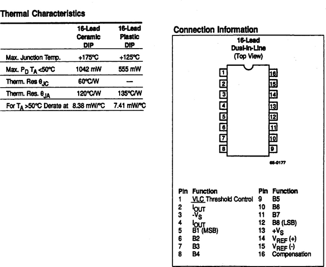
FIGURE 1-5 Connection information and thermal characteristics of typical DAC IC (Raytheon Semiconductor Data Book, 1994, p. 3-140)
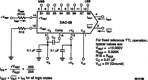
FIGURE 1-6 DAC-08 connected for basic positive-reference operation (Raytheon Semiconductor Data Book, 1994, p. 3-148)
1.2.1 Basic Design Requirements
The DAC-08 is a multiplying DAC in which the output current is the product of a digital number and the input reference current. This is somewhat different from the theoretic DAC of Fig. 1-2b, but the net result is the same. A digital or binary word is converted to an output current (which can be further converted to voltage by passing the current through a resistor or load).
In the circuit of Fig. 1-6, the reference current may be fixed or vary from 100 uA to 4 mA. The full-scale output current (IFS) is a linear function of the reference current (IREF) and is given by IFS = (255/256) × IREF, where IREF = 114. In the positive-reference application shown, the external reference forces current through R14 into the +Vref terminal (pin 14) of the reference amplifier (Fig. 1-4). If required, a negative reference may be applied to the – Vref terminal (pin 15). This negative-reference connection has the advantage of a very high impedance presented at pin 15. The voltage at pin 14 is equal to and tracks the voltage at pin 15. In some cases, R15 can be eliminated with only minor increases in tracking error. R15 is used to cancel any input bias current errors in the reference amplifier. Note that the reference amplifier is essentially an op amp (operational amplifier) and requires all of related design considerations (input bias current, phase margin correction). If you are not familiar with op-amp design problems, read my Simplified Design of IC Amplifiers (Newnes, 1996).
Figure 1-7 shows how bipolar references can be accommodated. Either Vref or pin 15 can be offset. The negative common-mode range of the reference amplifier is given by VCM = − VS plus (IREF × 1k) plus 2.5 V. The positive common-mode range is +VS less 1.5 V. When the reference is DC, a reference bypass capacitor is recommended. If a regulated power supply is used as a reference, R14 should be split into two resistors with the junction bypassed to ground with a 0.1-μF capacitor. (A 5-V TTL-logic supply is not recommended as a reference.)

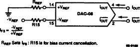
Figure 1-8 shows how the full-scale circuit can be adjusted. In most cases, this is not necessary because of the close relationship between IREF and IFS. It is also possible to adjust full-scale by substituting a potentiometer for R14. However, this is not recommended because of the temperature-coefficient (TC) effects of a potentiometer.
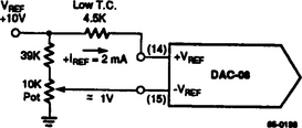
FIGURE 1-8 Typical full-scale adjustment circuit for DAC-08 (Raytheon Semiconductor Data Book, 1994, p. 3-148)
Figure 1-9 shows the basic negative reference operation. Using lower values of reference current reduces negative power-supply current and increases reference-amplifier negative common-mode range. The recommended range for operation with a DC reference current is +0.2 mA to +4.0 mA. With either positive or negative reference operation, the reference amplifier must be compensated by a capacitor Cc connected from pin 16 to –VS, as shown in Fig. 1-6. If the reference is a fixed DC voltage, a value of 0.01 μF is recommended for the compensating capacitor. If the reference is AC or pulse, the value of Cc must be selected as described in Section 1.2.2.
1.2.2 Reference Amplifier Compensation
The value of capacitor Cc depends on the impedance presented to pin 14. For example, for R14 values of 1.0, 2.5, and 5.0 k, the minimum values of Cc are 15, 37, and 75 pF, when the reference is AC. Larger values of R14 require proportionately increased values of Cc to ensure proper phase margin. When the reference input is a pulse, use a low value for R14. This makes it possible to use smaller values for Cc.
If pin 14 is driven by a high impedance, such as a transistor current source, the recommended values for compensation do not apply. This is because the reference amplifier must be heavily compensated. Unfortunately, such compensation decreases overall bandwidth and slew rate (as is the case when an op amp is heavily compensated). As a point of reference, for an R14 of 1 k and a Cc of 15 pF, the reference amplifier slews at 4.0 mA/μs, and results in a transition from IREF = 0 to IREF = 2.0 mA in 500 ns.
When a low full-scale transition time is critical, use 200 ohms for R14, and make Cc = 0. Under these conditions, full-scale transition (0 to 2.0 mA) occurs in 120 ns. This produces a slew rate of 16 mA/μs.
1.2.3 Input Circuits
The DAC-08 can be interfaced directly to all popular logic families with a maximum of noise immunity. This is because of the large input swing capability, a 2.0-μA logic-input current, and adjustable logic-threshold voltage. For example, when the supply is − 15 V, the logic inputs can swing between − 10 V and +18 V. This allows direct interface with +5 V CMOS (complementary metal oxide semiconductor) logic, even when the supply is +5 V. The minimum input-logic swing and minimum logic threshold are given by: supply plus (IREF × 1 k) plus 2.5 V.
The logic threshold can be adjusted over a wide range by placing an appropriate voltage at the logic threshold control VLC (pin 1). The logic-threshold voltage VTH is nominally 1.4 V above VLC. For TTL and DTL interface, simply ground pin 1 as shown in Fig. 1-6. For interfacing ECL, an IREF of 1 mA is recommended. Figure 1-10 shows typical interface circuits for ECL (emitter-coupled logic), CMOS, and PMOS/NMOS.

FIGURE 1-10 Typical interface circuits for ECL, CMOS, and PMOS/NMOS (Raytheon Semiconductor Data Book, 1994, p. 3-150)
Note that pin 1 will source or sink 100 μA (typical), so external circuits should be designed to accommodate this current. When a fast settling time (Section 1.2.7) is essential, keep in mind that the fastest times are obtained when pin 1 sees a low impedance. For example, pin 1 can be connected to a 1-k divider and bypassed to ground with a 0.01 μF capacitor.
1.2.4 Output Circuits
Figures 1-11 through 1-13 show typical unipolar, bipolar, and offset-binary output circuits and the relationships between digital inputs and voltage/current outputs. As shown, both true and complemented output sink currents are provided where IOUT + ![]() = IFS.
= IFS.
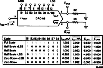
FIGURE 1-11 DAC-08 connected for basic unipolar-negative operation (Raytheon Semiconductor Data Book, 1994, p. 3-149)
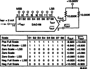
FIGURE 1-12 DAC-08 connected for basic bipolar-output operation (Raytheon Semiconductor Data Book, 1994, p. 3-149)

FIGURE 1-13 DAC-08 connected for basic offset-binary operation (Raytheon Semiconductor Data Book, 1994, p. 3-149)
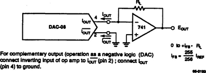
Current appears at the true output when a 1 is applied to each logic input. As the binary count increases, the sink current at pin 4 increases proportionally (a positive-logic DAC). When a 0 is applied to any input bit, that current is turned off at pin 4 and turned on at pin 2. A decreasing logic count increases IOUT proportionally (a negative-logic or inverted-logic DAC).
Both outputs can be used simultaneously, and both have a wide voltage compliance. This allows fast current-to-voltage conversion through a resistor tied to ground or other voltage source (Figs. 1-11, 1-12). Positive compliance is 36 V above the negative supply and is independent of the positive supply. Negative compliance is given by supply voltage plus (IREF × 1 k) plus 2.5 V.
The dual outputs allow double the usual peak-to-peak load swing when driving loads in a quasidifferential manner. This feature is especially useful in cable-driver or CRT-deflection circuits and other balanced applications, such as driving center-tapped coils and transformers.
If one of the outputs is not required, it must still be connected to ground or to a point capable of sourcing IFS. Do not leave an unused output pin open. This is shown in Figs. 1-14 and 1-15 where the pin-4 output is connected to an op amp. With these circuits, the output impedance is lowered to a value determined by the op amp, not the DAC. In both cases, the unused DAC output is connected to ground and the converted output is taken from the op amp.

1.2.5 Power Supply Requirements
Symmetric supplies are not required. However, the DAC-08 will operate satisfactorily with standard ±5.0-V supplies, or any supply combination in which the total is 9 V to 36 V. If ±5.0 V is used, the IREF should not exceed 1 mA. Keep in mind that low reference-current operation decreases power consumption and increases negative compliance, reference-amplifier negative common-mode range, negative-logic input range, and negative-logic threshold range. This is shown in the various graphs of Fig. 1-16.

FIGURE 1-16 Typical performance characteristics of DAC-08 (Raytheon Semiconductor Data Book, 1994, p. 3-145)
Power consumption (PD) can be calculated as follows: (1+ × +VS) + (I– × –VS) + (2 IREF × –VS). Supply current (I) is constant and independent of input-logic states. This reduces the size of power-line bypass capacitors.
1.2.6 Temperature Characteristics
The nonlinearity and monotonicity specifications of the DAC-08 are guaranteed to apply over the entire rated operating temperature range (Fig. 1-5). (See Chapter 2 for a discussion of monotonicity.) Full-scale output-current drift is typically ± 10 ppm/°C. Zero-scale output current and drift are essentially negligible to ½ LSB.
To achieve minimum overall full-scale drift, the temperature coefficient of the reference resistor (Fig. 1-6) should match and track that of the output resistor. Settling times (Section 1.2.7) decrease approximately 10% at−55°C. At +125°C, an increase of about 15% is typical.
1.2.7 Settling Time
Figure 1-17 shows a settling-time test circuit for the DAC-08. This circuit also can be used for many other DACs with slight modification. Settling time is often the single most critical factor in DAC operation because it determines overall speed of the digital-to-voltage conversion. The DAC-08 requires 35 ns for each of the 8 data bits. Settling time to within ½ LSB is therefore 35 ns, with each progressively larger bit taking successively longer. The MSB settles in 85 ns, determining the overall settling time of 85 ns. Figure 1-16 shows a typical oscilloscope response for measurement of full-scale settling time, indicating about 85 ns from the start of the logic input to the point where the output settles to a constant level. Settling to 6-bit accuracy requires about 65 to 70 ns.

FIGURE 1-17 Settling-time test circuit for DAC-08 (Raytheon Semiconductor Data Book, 1994, p. 3-151)
As in the case of all digital ICs, the fastest operation is obtained using short leads, minimum output capacitance, minimum load resistance, and adequate bypassing for the supply. The bypass need not be electrolytic because supply current drain is independent of the input logic state. The 0.1-μF bypass capacitors shown provide full transient protection. The output capacitance of the DAC-08 (including the package) is about 15 pF. Therefore the output RC (resistance-capacitance) time constant dominates settling time when the load is greater than 500 ohms.
Measurement of settling time requires the ability to accurately resolve ±4.0 μA, so a 1-k load is needed to provide adequate drive (±0.4 V) for most scopes. The circuit of Fig. 1-17 uses a cascade design to allow driving the 1-k load with less than 5 pF of parasitic capacitance at the measurement node. At IREF values of less than 1 mA, excessive RC damping of the output is difficult to prevent if adequate sensitivity is maintained. However, the major carry from 01111111 to 10000000 provides an accurate indicator of settling time. This code change does not require the normal 6.2 time constants to settle to within ± 0.2% of the final value, so settling times can be observed at lower values of IREF.
Settling time remains essentially constant for IREF values down to 1 mA, with gradual increases for lower IREF values. The main advantage of higher IREF values is the ability to obtain a given output level with lower load resistors, reducing the output RC time constant. Switching transients are generally low and can be further reduced by small capacitive loads at the output. Of course, this increase in RC time constant does increase settling time.
1.3 Typical ADC IC
Figure 1-18 shows the functional block diagram of typical ADC ICs (the industry standard MAX174 and MX574A/MX674A). Figure 1-19 shows the pin functions. The ICs are complete 12-bit ADCs that combine high speed, low-power consumption, and on-chip clock and voltage reference. The maximum conversion times are 8 ms (MAX714), 15 ms (MX674A), and 25 ms (MX574A).

FIGURE 1-18 Functional block diagram of typical ADC IC (Maxim New Releases Data Book, 1992, p. 7-81)

1.3.1 Basic Converter Operation
These ICs use the successive-approximation technique described in Section 1.1.9 to convert an unknown analog input to a 12-bit digital output code. Compare the circuit of Fig. 1-18 with that of Fig. 1-3c. The control logic function of Fig. 1-18 provides easy interface with most microprocessors. The internal voltage-output DAC is controlled by an SAR (see Section 1.1.9). The analog input is connected to the DAC output with a 5-k resistor for the 10-V input and a 10-k resistor for the 20 V input. The comparator is essentially a zero-crossing detector, with the output fed back to the SAR input. Figure 1-20 shows the equivalent of the analog input circuit.
In the IC of Fig. 1-18, the SAR is set to half scale as soon as a conversion starts. The analog input is compared to ½ of the full-scale voltage. The bit is kept if the analog input is greater than half scale or dropped if smaller. The next bit (bit 10) is then set with the DAC output either at ¼ scale, if the MSB is dropped, or ¾ scale if the MSB is kept. The conversion continues in this manner until the LSB is tried. At the end of the conversion, the SAR output is latched into the output buffers.
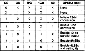
1.3.2 Digital Control
Operation of the ICs is controlled by the CE (chip enable), ![]() (chip select), and R/
(chip select), and R/![]() lines. Figure 1-21 shows the truth table for these lines and the A0 (pin 4) and 12/8 (pin 2) lines. While both CE and
lines. Figure 1-21 shows the truth table for these lines and the A0 (pin 4) and 12/8 (pin 2) lines. While both CE and ![]() are asserted, the state of R/
are asserted, the state of R/![]() selects whether a conversion (R/
selects whether a conversion (R/![]() = 0) or a data read (R/
= 0) or a data read (R/![]() = 1) is in progress. The register-control inputs,
= 1) is in progress. The register-control inputs, ![]() and A0, select the data format and conversion length. A0 is usually tied to the LSB of the address bus. To perform a full 12-bit conversion, set A0 low during a convert start. For a shorter 8-bit conversion, A0 must be high during a convert start.
and A0, select the data format and conversion length. A0 is usually tied to the LSB of the address bus. To perform a full 12-bit conversion, set A0 low during a convert start. For a shorter 8-bit conversion, A0 must be high during a convert start.
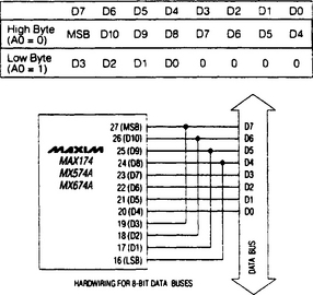
1.3.3 Output Data Formats
Figure 1-22 shows the data format for an 8-bit bus, including typical hardwiring. Output data bits are formatted according to the control signal on the 12/8 input. If pin 2 is low, the output is a word broken into two 8-bit bytes. If pin 2 is high, the output is one 12-bit word. During a data read, A0 selects whether the three-state buffers contain the 8 MSBs (A0 = 0) or the 4 LSBs (A0 = 1) of the digital result. The 4 LSBs are followed by four trailing 0s (zeros). A0 can change state while a data-read operation is in effect.
To begin a conversion, the microprocessor must write to the ADC address. Then, because a conversion usually takes longer than a single clock cycle, the microprocessor must wait for the ADC to complete the conversion. Valid data bits are made available only at the end of the conversion, which is indicated by STS (pin 28k the output status). STS can be either polled or used to generate an interrupt upon completion. Or the microprocessor can be kept idle by means of insertion of the appropriate number of NOP (no operation) instructions between the conversion-start and data-read commands.
After the conversion is completed, data can be obtained by the microprocessor. The ICs have the required logic for 8-, 12-, and 16-bit bus interfacing (as determined by the ![]() input). If pin 2 is high, the ICs are configured for a 16-bit bus. Data lines D0-D11 can be connected to the bus as either the 12 MSBs or the 12 LSBs. The other 4 bits must be masked out in software.
input). If pin 2 is high, the ICs are configured for a 16-bit bus. Data lines D0-D11 can be connected to the bus as either the 12 MSBs or the 12 LSBs. The other 4 bits must be masked out in software.
For 8-bit bus operation, pin 2 is low. The format is left-justified and the even address (A0 low) contains the 8 MSBs. The odd address (A0 high) contains the 4 LSBs, followed by four trailing 0s. There is no need to use a software mask when the ICs are connected to an 8-bit bus. (Note that the output cannot be forced to a right-justified format by rearranging the data lines on the 8-bit bus interface.)
1.3.4 Convert-Start Timing with Full Microprocessor Control
Figure 1-23 shows the convert-start timing when the ICs are under full microprocessor control. It is essential that R/![]() must be low before asserting both CE and
must be low before asserting both CE and ![]() . If R/
. If R/![]() is high, a brief read operation occurs. This could result in system-bus contention (a bus fight). Either CE or
is high, a brief read operation occurs. This could result in system-bus contention (a bus fight). Either CE or ![]() can be used to initiate conversion. However, CE is recommended because it is shorter by one propagation delay than
can be used to initiate conversion. However, CE is recommended because it is shorter by one propagation delay than ![]() and is the faster input of the two.
and is the faster input of the two.
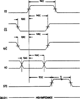
Once STS goes high, signaling that a conversion has started, all convert-start commands have no effect until the conversion is complete. The output buffers cannot be enabled during a conversion.
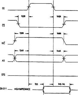
1.3.5 Read Timing with Full Microprocessor Control
Figure 1-24 shows the read-cycle timing. During data reading, access time is measured from when CE and R/![]() are both high. Access time is extended 10 ns if
are both high. Access time is extended 10 ns if ![]() used to initiate a read.
used to initiate a read.
1.3.6 Stand-Alone Operation
For systems that do not use or require full-bus interface (under microprocessor control, when a CE or ![]() signal or both are available), ICs can be operated in a standalone mode directly linked through dedicated ports. The R/
signal or both are available), ICs can be operated in a standalone mode directly linked through dedicated ports. The R/![]() input is used to control the IC; the STS output provides an indication of conversion completion. To operate in stand-alone,
input is used to control the IC; the STS output provides an indication of conversion completion. To operate in stand-alone, ![]() and A0 hardwired low, with CE and
and A0 hardwired low, with CE and ![]() wired high.
wired high.
In stand-alone, R/![]() is set low to enable the three-state buffers. Conversion starts when R/
is set low to enable the three-state buffers. Conversion starts when R/![]() is set high. This allows either a high-pulse or low-pulse control signal to be applied at R/
is set high. This allows either a high-pulse or low-pulse control signal to be applied at R/![]() .
.
Figure 1-25 shows the timing for low-pulse control during stand-alone. In this mode, the outputs (in response to the falling edge of R/![]() ) are forced into the high-impedance state. The outputs return to valid-logic levels after the conversion is complete. The STS output goes high (following the R/
) are forced into the high-impedance state. The outputs return to valid-logic levels after the conversion is complete. The STS output goes high (following the R/![]() falling edge) and returns low when the conversion is complete.
falling edge) and returns low when the conversion is complete.
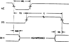
FIGURE 1-25 Timing for low-pulse control during stand-alone (Maxim New Releases Data Book, 1992, p. 7-90)
Figure 1-26 shows the timing for high-pulse control during stand-alone mode. In this mode, the output data lines are enabled when R/![]() is high. The next conversion starts with the falling edge of R/
is high. The next conversion starts with the falling edge of R/![]() . The data lines then return and remain in the high-impedance state until another high pulse is applied to R/
. The data lines then return and remain in the high-impedance state until another high pulse is applied to R/![]() .
.

1.3.7 Power Supply Requirements and Physical Layout
Figure 1-27 shows the recommended power-supply grounding. The ground-reference point for the on-chip reference is AGND (pin 9), which should be connected to the analog-reference point of the system. The analog and digital grounds should be connected together at the IC package to obtain maximum accuracy in high digital-noise environments. If the situation allows (low digital noise), the grounds can be connected to the most accessible ground-reference point, but the analog-power return is preferred.

FIGURE 1-27 Recommended power-supply grounding for typical ADC IC (Maxim New Releases Data Book, 1992, p. 7-90)
Figure 1-28 shows the recommended power-supply bypassing. The power supplies must be filtered, well regulated, and free from high-frequency noise. If they are not, unstable output codes can result, especially if switching spikes are present. Do not use switching power supplies for applications requiring 12-bit resolution. (A few mV of noise converts to several error counts in a 12-bit ADC.)
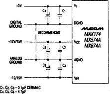
FIGURE 1-28 Recommended power-supply bypassing for typical ADC IC (Maxim New Releases Data Book, 1992, p. 7-91)
All power-supply pins should use supply decoupling capacitors connected with short leads to the pins. The VCC and VEE pins should be decoupled directly to AGND. A 4.7-μF tantalum capacitor in parallel with a 0.1-μF disk ceramic is recommended for decoupling.
ICs are designed for use on PC (printed circuit) boards. Wire-wrap boards are not recommended. Board layout should be made so that digital and analog signal lines are kept separated from each other as much as possible. Care should be taken not to run analog and digital lines parallel to each other or to run digital lines directly underneath the ICs (as is the case with any good analog-digital board layout).
1.3.8 Internal Reference
As shown in Fig. 1-18, the ICs have an internal buried-zener reference that provides a 10-V, low-noise, and low-temperature-drift output (at pin 8). An external reference voltage can also be used (at pin 10). When using ± 15-V supplies, the internal reference can source up to 2 mA (in addition to the BiPOFF and REFin inputs) over the entire operating temperature range. With ± 12-V supplies, the reference can drive the BiPOFF and REFin inputs over temperature, but cannot drive an additional load.
1.3.9 Analog Inputs
The input leads to AGND and 10Vin or 20VIN should be as short as possible to minimize noise pickup. Use shielded cables if long leads are required.
When the 20Vin is used as the analog input, load capacitance on the 10Vin pin must be minimized. Especially on the faster MAC174, leave the 10Vin pin open to minimize capacitance and to prevent linearity errors caused by inadequate settling time.
The amplifier used to drive the analog input must have low DC output impedance for low full-scale error. In addition, low AC output impedance is required because the analog input current is modulated at the clock rate during the conversion. (The output impedance of an amplifier is the open-loop output impedance divided by the log gain at the frequency of interest.)
The internal clock rate for the MAX714 is 2 MHz. This requires faster amplifiers such as the OP-27, AD711, or OP-42. The approximate internal clock rate for the MX574A is 600 kHz, with 1 MHz for the MX674A. An amplifier such as the MAX400 can accommodate these speeds.
1.3.10 Track-and-Hold Interface
The analog input to these ADCs must be stable to within ½ LSB during the entire conversion for specified 12-bit accuracy. This limits the input-signal bandwidth to a few Hz for sine-wave input (even with the faster MAX174). A track-and-hold amplifier should be used for higher bandwidth signals.
The STS output can be used to provide the Hold signal to the track-and-hold (T/H) amplifier. However, because the internal DAC is switched at about the same time as the conversion is initiated, the switching transients at the output of the T/H DAC switches might result in code-dependent errors. It is recommended that the Hold signal to the T/H amplifier precede a conversion or be coincident with the conversion start.
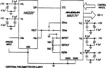
The first bit decision by the ADC is made approximately 1.5 clock cycles after the start of conversion. This is 2.5 μs, 1.5 μs, and 0.8 μs for the MX574A, MX674A and MAX174, respectively. The T/H hold settling time must be less than these times. Figures 1-29 and 1-30 show recommended T/H circuits for the MX574A/674A and MAX174, respectively.

1.3.11 Input Ranges and Digital Output Codes
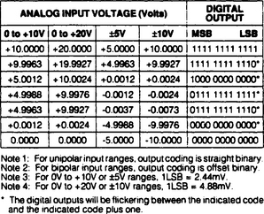
Figure 1-31 shows the possible input ranges and “ideal” transitions voltages. End-point errors can be adjusted in all ranges (see Sections 1.3.12 and 1.3.13).
1.3.12 Typical Unipolar Input
Figures 1-32 and 1-33 show the ideal transfer function and input connections, respectively, for unipolar input operation. In many cases, the gain (full scale) and offset need not be calibrated. This is because all internal resistors of the ADCs are trimmed for absolute calibration. (The absolute accuracy for each grade of ADC is given in the data-sheet specifications.)
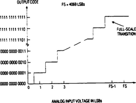

For a 0-V to +10-V input range, the analog input is connected between AGND and 10Vin, as shown in Fig. 1-33. For a 0-V to + 20-V input range, connect the analog input between AGND and 20Vin. Note that these ADCs can easily handle input signals beyond the supply voltage.
Should a 10.24-V input range be required, connect a 200-ohm trimmer in series with 10Vin. For a full-scale input range of 20.48 V, use a 500-ohm trimmer in series with 20Vin. The nominal input impedance into 10Vin is 5 k, and into 20Vin is 10 k.
If the full-scale input and offset need not be trimmed, delete R1, R2, and the related wiring shown in Fig. 1-33. Connect BIPoff directly to AGND. Connect a 50-ohm metal-film resistor (±1%) between REFout and REFin.
If the full-scale input and offset must be trimmed, use the connections of Fig. 1-33 and proceed as follows. Adjust the offset first. Apply ½ LSB (see Fig. 1-31 for voltages) at the analog input and adjust R1 until the digital output code flickers between 0000 0000 0000 and 0000 0000 0001. Then apply full-scale less 3/2 LSB (Fig. 1-31) at the analog input and adjust R2 until the output code changes between 1111 1111 1110 and 1111 1111 1111 (see Section 1.4 for a discussion of ADC trimming and adjustment).
1.3.13 Typical Bipolar Input
Figures 1-34 and 1-35 show the ideal transfer function and input connections, respectively, for bipolar input operation. The full scale and offset need not be calibrated for all applications because of the internal-resistor accuracy and trimming. One or both of the trimmers (R1, R2) can be replaced with a 50-ohm (±1%) resistor if external trimming is not required. The analog input ranges can be either ±5 V or ± 10 V, as needed.
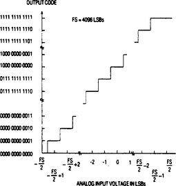

If the full-scale and offset must be trimmed, use the connections of Fig. 1-35 and proceed as follows. Adjust the offset first. Apply ½ LSB above negative full-scale (see Fig. 1-31) at the analog input and adjust R1 until the digital output code flickers between 0000 0000 0000 and 0000 0000 0001. Then apply a voltage 3/2 LSB below positive full-scale (Fig. 1-31) at the analog input and adjust R2 until the output code changes between 1111 1111 1110 and 1111 1111 1111.
1.4 Basic ADC/DAC Testing and Troubleshooting
This section is devoted to digital testing and troubleshooting basics. The testing and troubleshooting for specific data converter ICs are given in the related chapters. It is assumed that you are already familiar with digital troubleshooting at a level found in Lenk’s Digital Handbook (McGraw-Hill, 1993). However, the following paragraphs summarize both testing and troubleshooting as they relate to ADC and DAC ICs.
1.4.1 Digital Circuit Testing and Troubleshooting
Both testing and troubleshooting for the data converters in this book can be performed with conventional test equipment such as meters, generators, and scopes. However, a logic or digital probe and a digital pulser can make life much easier if you must regularly test and troubleshoot data converters (or any other digital device). So we start with brief descriptions of the probe and pulser.
1.4.2 Logic or Digital Probe
Logic probes are used to monitor in-circuit pulse or logic activity. By means of a simple lamp indicator, a logic probe shows you the logic stage of the digital signal and allows detection of brief pulses (the ones you might miss with a scope). Logic probes detect and indicate high and low (1 or 0) logic levels and intermediate or “bad” logic levels (indicating an open circuit) at the terminals of a logic element such as an ADC or DAC.
Not all logic probes have the same functions, and you must learn the operating characteristics for your particular probe. For example, on the more sophisticated probes, the indicator lamp can give any of four indications: off, dim (about half brilliance), bright (full brilliance), or flashing on and off.
The lamp is normally in the dim state and must be driven to one of the other three states by voltage levels at the probe tip. The lamp is bright for inputs at or above the 1 state and is off for inputs at or below 0. The lamp is dim for voltages between the 1 and 0 states and for open circuits. Pulsating inputs cause the lamp to flash at about 10 Hz (regardless of the input pulse rate). The probe is particularly effective when used with the logic pulser.
1.4.3 Logic Pulser
The hand-held logic pulser (similar in appearance to the logic probe) is an in-circuit stimulus device that automatically outputs pulses of the required logic polarity, amplitude, current, and width to drive lines and other test points high or low. A typical pulser has several pulse burst and stream modes.
Logic pulses are compatible with most digital devices. Pulse amplitude depends on the equipment supply voltage, which is also the supply voltage for the pulser. Pulse current and pulse width depend on the load being pulsed. A switch controls the frequency and number of pulsers that are generated. A flashing LED (light-emitting diode) indicator on the pulser tip indicates the output mode.
The logic pulser forces overriding pulses into lines or test points, and it can be programmed to output single pulses, steady pulse streams, or bursts. The pulser can be used for ICs to be enabled or clocked. The circuit inputs also can be pulsed while the effects on the circuit outputs are observed with a logic probe.
1.4.4 General Digital Troubleshooting Sequence
The following troubleshooting tips are not limited to ADCs and DACs. They also apply to all digital circuits in which most of the components are contained within ICs.
1.4.5 Power and Ground Connections
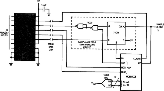
The first step in tracing problems in a digital circuit with ICs is to check all power and ground connections to the ICs. Many ICs have more than one power and one ground connection. For example, the LTC1090 in Fig. 1-36 requires +5 V at the Vcc pin and ground at the V – pin. The IC also has both a digital ground (DGND) and an analog ground (AGND), as well as a common (COM) pin, and a minus-reference (REF–) pin that must be grounded. The REF+ pin must also be connected to 5-V power. If any of these power or ground connections is absent or abnormal, the IC cannot operate properly.
1.4.6 Reset, Chip-Select, and Start Signals
With all power and ground connections confirmed, check that all the ICs receive reset, chip-select, and start signals, as required. For example, the DAC-4881 in Fig. 1-37 requires a chip-select at pin 1 and address-decode signals at pins 2 and 28. Likewise, the ADC0808/0809 in Fig. 1-38 requires start, address latch enable (ALE), end-of-conversion (EOC), and output enable signals (Fig. 1-38c) from a microprocessor or control logic. If any of these signals is absent or abnormal (for example, incorrect amplitude, improper timing) circuit operation comes to an immediate halt.


FIGURE 1-37 Typical control signals for digital IC (Raytheon Semiconductor Data Book, 1994, p. 6-48)
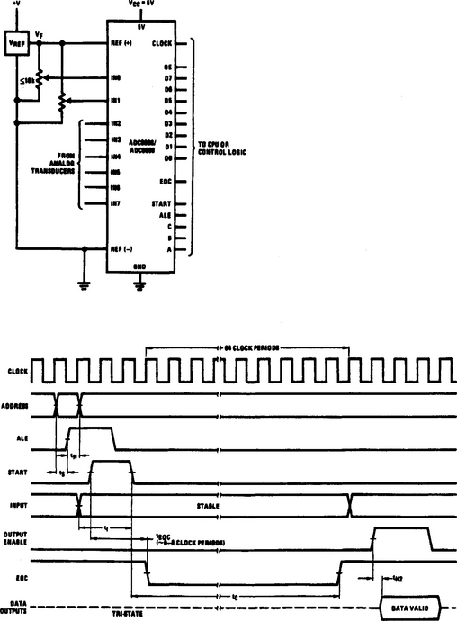
FIGURE 1-38 Typical control signals and timing diagram for digital IC (National Semiconductor, Linear Applications Handbook, 1994, p. 531/532)
In some cases, control signals to digital ICs are pulses (usually timed in a certain sequence), whereas other control signals are steady (high or low). If any of the lines carrying the signals to the IC are open, shorted to ground, or to power (typically +5 V or +12 V), the IC will not function. So if you find an IC pin that is always high, always low, or apparently is connected to nothing (floating), check the PC traces or other wiring to that pin carefully. This applies to all control pins, unless the circuit calls for the control function to be steady (such as a steady + 5 V on a pin to turn a circuit on). For example, if the DAC-4881 is connected as an 8-bit with complementary input DAC as shown in Fig. 1-37, the chip-select (pin 1) must receive a write (![]() ) signal, and the address-decode pins must receive address bits from the microprocessor.
) signal, and the address-decode pins must receive address bits from the microprocessor.
1.4.7 Clock Signals
Most digital ICs require clocks. For example, Fig. 1-38c shows the clock periods for the ADC in Fig. 1-38. In this case, the clock comes from an external source. In other cases, the clock is part of the circuit. In general, the presence of pulse activity on any pin of a digital IC indicates the presence of a clock, but do not count on it. Check directly at the clock pins (all ICs that require a clock typically are connected to the same clock source).
It is possible to measure the presence of a clock signal with a scope or logic probe. However, a frequency counter provides the most accurate measurement. If any ICs do not receive required clock signals, the IC cannot function. On the other hand, if the clock is off frequency, all of the ICs might appear to have a clock signal, but the IC function can be impaired. Notice that crystal-controlled clocks do not usually drift far off frequency but can go into some overtone frequency (typically a third overtone) beyond the capacity of the IC.
1.4.8 Input-Output Signals
When you are certain that all ICs are good and have proper power and ground connections and that all control signals (such as reset, chip-select) and clock signals are available, the next step is to monitor all input and output signals at each IC. This can be done with either a scope or a probe. The following are some examples that apply to ADCs and DACs.
1.4.9 Basic ADC Testing and Troubleshooting
ADCs can be tested by applying precision voltages at the input and monitoring the output for corresponding digital values. For example, a fixed voltage between 0 and +10 V can be applied to the noninverting input of the 4805 in Fig. 1-39, and the corresponding value can be read out at the lines between the SAR-2504 and DAC-6012. The lines should go to +5 V for a digital 1 and to ground or 0 V for a digital 0. There is also a serial digital output at the D0 pin of the 2504. This output must be monitored with a scope.
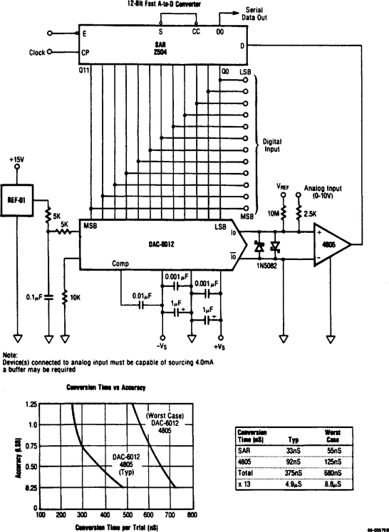
The rate at which the conversions are made is controlled by the clock at the CP pin of the 2504. Notice that the start (S) pin of the 2504 is connected to the conversion-complete (CC) pin to provide continuous digital outputs for the analog input. In the circuit of Fig. 1-39, the start pin must receive a conversion command from an external source (typically a microprocessor), whereas the conversion-complete becomes an output to the microprocessor (indicating status and conversion complete or not complete).
If the output readings of the ADCs in this book are slightly off, try correcting the problem by means of adjustment. In the circuit of Fig. 1-39, the Vref voltage (at the noninverting input of the 4805) can be varied for 0 (0 V at the analog input should make all digital outputs ground or 0 V). Also, REF-01 can be trimmed for full-scale output. This is done by connecting a 10-k pot between the output (pin 6) of the REF-01 and ground (pin 4). The wiper of the pot is connected to trim (pin 5) of the REF-01. The accuracy of this circuit depends on the precision of the two 5-k resistors between the REF-01 and pin 14 of the DAC-6012 and on the 2.5-k resistor at the analog input.
1.4.10 Basic DAC Testing and Troubleshooting
DACs can be tested by applying digital inputs and monitoring the output for corresponding voltages. For example, the B1 through B10 inputs of the DAC-10 can be connected to ground (for a 0) or to +5 V (for a 1), and the output can be monitored with a precision voltmeter at pins 2 and 4 in the circuit of Fig. 1-40. If both voltages are slightly off, suspect the 2.00-mA references. If one of the output voltages is slightly off, suspect the corresponding 1.25-k resistors. If the output voltages are absent or way off, suspect the DAC-10
