
Simplified Design with a Flash ADC
This chapter is devoted to simplified-design approaches for a typical video-frequency (VF) or high-speed flash-type ADC. All of the general design information in Chapters 1 through 3 applies to the examples in this chapter. The circuits in this chapter can be used immediately the way they are or, with alterations in component values, as a basis for simplified design of similar data-converter applications. The chapter concludes with a high-speed interface circuit.
5.1 General Description of ADC
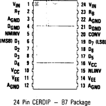
Figure 5-1 shows the functional block diagram for the ADC (a Raytheon Semiconductor TDC1147). The pin configuration is shown in Fig. 5-2. The package interconnections are shown in Fig. 5-3.


This 7-bit flash ADC has no “pipeline delay” between sampling and valid data. The output-data register normally found on flash ADCs is bypassed, allowing data to transfer directly to output drivers from the encoding-logic section of the circuit. (The TDC1147 is function- and pin-compatible with the Raytheon Semiconductor TDC1047, which does have an output-data register.) The TDC1147 requires only one clock pulse to perform the complete conversion operation. Conversion time is guaranteed to be less than 60 ns. The TDC1147 operates accurately at sampling rates up to 15 Msps (15 million samples per second), and has an analog bandwidth of 7 MHz, as shown in Fig. 5-4. Linearity errors are guaranteed to be less than 0.4% over the operating temperature range.
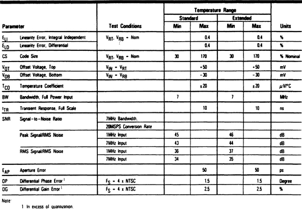
FIGURE 5-4 Performance characteristics for TDC1147 (Raytheon Semiconductor Data Book, 1994, p. 3-101)
The TDC1147 is fully TTL compatible, as shown in Figs. 5-3 and 5-5, and has 7-bit resolution with ½ LSB linearity. The output coding (Fig. 5-6) format can be selected. A sample-and-hold circuit is not required for any configuration.


5.2 Data-Converter Operation
As shown in Fig. 5-1, the TDC1147 has two functional sections: a comparator array and encoding logic. The comparator array compares the input signal with 127 reference voltages to produce an N-of-127 code. (Such a code is sometimes called the thermometer code because all comparators referred to voltages more positive than the input signal will be off, and those referred to voltages more negative than the input will be on.) The encoding logic converts the N-of-127 code into binary or offset two’s complement and can invert either output code. The coding function is controlled by DC signals on pins NMinv and NLinv.
5.3 Power Requirements
The TDC1147 operates from two supply voltages, +5.0 V and −5.2 V. The return path for ICC (the current drawn from the +5.0-V supply) is DGND. The return path for IEE (the current drawn from the −5.2-V supply) is AGND. All power and ground pins must be connected.
5.4 Reference Voltage Requirements
The TDC1147 requires an external reference voltage applied at the input reference-resistor chain. The range of analog input voltages to be converted into digital form is set by the external reference voltages. (VRB is the voltage at the bottom of the chain, and VRT is the voltage at the top of the chain.) The voltage applied across the reference resistor chain (VRT – VRB) must be between 0.8 V and 1.2 V. VRB and VRT should be between +0.1 V and −1.1 V. VRT should be more positive than VRB within the range. The nominal voltages are VRT = 0.00 V and VRB = −1.00 V.
The reference voltages can be varied dynamically up to 7 MHz. Because of slight variations in the reference current with clock and input signals, the RT and RB (top and bottom of reference input chain) points should be low impedance. For circuits in which the reference is not varied, a bypass capacitor to ground is recommended. If the reference inputs are varied dynamically, such as with an AGC (automatic gain control) function, use a low-impedance reference-voltage source.
5.5 Output Coding Control
Two function-control pins, NMinv and NLinv, are provided to control output coding. These controls require DC (steady state) signals and allow the output coding to be either straight binary or offset two’s complement, in either true or inverted sense (Fig. 5-6).
5.6 Initiating a Conversion
The TDC1147 uses a convert (CONV) input signal to initiate the ADC process. Unlike other flash ADCs, which have a one-clock-cycle pipeline delay between sampling and output-data, the TDC requires only a single pulse to perform the entire conversion operation.
As shown in Fig. 5-7, the analog input is sampled (the comparators are latched) within the maximum sampling time offset (tSTO). Data bits from that sample become valid after a maximum output delay time (tD). Data bits from the previous sample are held at the outputs from a minimum output hold time (tHO). This allows data bits from the TDC1147 to be acquired by an external register or other circuit. There are minimum time requirements for the HIGH and LOW portions (tPWH, tPWL) of the CONV waveform, and all output-timing specifications are measured with respect to the rising edge of CONV (Fig. 5-7).

5.7 Analog Inputs
The TDC1147 uses latching comparators that cause the input impedance to vary slightly with the signal level. For best results, both Vin pins must be used, and the source impedance of the driving signal (analog input) must be less than 30 ohms.
Input signals will not damage the TDC1147 if the signals remain within the range of Vee (typically−5.2 V) and +0.5 V. If the input signal is between the Vrt and Vrb references, the output will be a binary number between 0 and 127 inclusive. An input signal outside this range indicates either full-scale positive or full-scale negative, depending on whether the signal is off-scale in the positive or negative direction.
5.8 Digital Outputs
The TDC1147 outputs are TTL compatible and capable of driving four low-power Schottky TTL (54/74 LS) unit loads. The outputs hold the previous data bits a minimum time (tHO) after the rising edge of the CONV signal. New data bits become valid after a maximum time (tD) after the rising edge of the CONV signal. The use of 2.2-k pull-up resistors is recommended at the digital outputs.
5.9 Calibration
Basic calibration of the TDC1147 requires that the voltages applied to the resistor chain, Vrt and Vrb, be adjusted to set the 1st and 127th thresholds. For example, assuming a 0-V to – 1-V input range, apply a−0.0039-V (½ LSB from 0 V) at the analog input and adjust Vrt for a digital output that toggles between 00 and 01. Thenapply−0.996 V (½ LSB from – 1-V) and adjust Vrb for toggling between codes 126 and 127.
This method of calibration requires that both ends of the resistor chain, RT and RB, be driven by variable voltage sources. Instead of adjusting Vrt, RT can be connected to the analog ground, and the 0-V end of the range can be calibrated with an input-amplifier offset control. (Such a configuration is described in Section 5.10.) When this alternative calibration is used, an offset error at the bottom of the resistor chain causes a slight gain error, which can be compensated for by varying Vrb. The bottom reference is a convenient point for gain adjust that is not in the analog signal path.
The offset voltages are generated by the parasitic resistance between the package pin and the actual resistor chain on the IC. These parasitic resistors are shown as R1 and R2 in Fig. 5-1. Calibration cancels all offset voltage, eliminating any offset and gain errors.
5.10 Typical Video Interface
Figure 5-8 shows a VF interface circuit for the TDC1147. (Note that a TDC1047 is shown. However, the TDC1147 and TDC1047 are pin compatible.) The circuit can be used to convert VF analog signals up to the limits defined in Fig. 5-4. Any of the digital-output formats shown in Fig. 5-6 can be selected with the proper control signals applied to pins 5 and 15 (NMinv and NLinv).
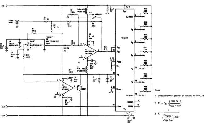
The analog amplifier U2 is a bipolar wideband op amp used to drive the ADC. Bipolar inputs can be accommodated by adjusting the OFFSET control R8. Zener U4 provides a stable reference for R8 as well as the GAIN control R9. U2 has a gain of – 1, providing the recommended 1-VP–P input for the ADC.
Variable capacitor C12 allows the frequency response of U2 to be adjusted for optimum performance, depending on the type of analog signal being converted (sine wave, step). C12 can be replaced with a fixed capacitor, if desired, after the circuit-board layout is set, and an optimum value (between 1 and 6 pF) is selected.
The circuit of Fig. 5-8 can be calibrated using the basic techniques described in Section 5.9. Use OFFSET control R8 to set Vrt, and GAIN control R9 to set Vrb. Note that Vrb is supplied by inverting amplifier U3 and transistor Q1. (The PNP transistor is used to provide a low-impedance source and is necessary to sink the current flowing through the reference-resistor chain.) After the 1st and 127th thresholds are set, adjust C12 as necessary for best performance (to accommodate the type of analog signal being converted).
Note that the degree of decoupling shown in Fig. 5-8 might not be required in all configurations. However, proper decoupling is recommended for all power supplies.