
Single-Chip Digital Multimeter
This chapter describes an integrating ADC (the MAX133/134) that contains the major components of a 3 ¾-digit digital multimeter (DMM) in a single IC. The ADC can also be used for data-acquisition systems such as data loggers and weigh scales. The internal resolution is ±40,000 counts. An extra digit is supplied as a guard digit to allow autozero or tare of a 4,000-count displayed reading to 1/10 of a displayed count. The conversion time is 50 ms.
The MAX133 and MAX134 differ only in their microprocessor interface. The MAX133 has a 4-bit multiplexed address-data bus, whereas the MAX134 has 3 separate address lines and a 4-bit bidirectional data bus. Both devices can be used with 4-, 8-, and 16-bit microprocessors.
When controlled by a microprocessor, the IC can perform autoranging measurements from ±400.0 mV to ±4000 V full scale. External attenuator resistors are required, but range switching is performed by the ADC. The power supply is typically a 9-V battery, or ±5 V. Operating current is typically 100 μA, with a 25-μA standby current.
10.1 System Considerations
Figure 10-1 shows the typical operating circuit and pin configuration. Figure 10-2 shows a test circuit and basic DMM voltage and current modes. Figure 10-3 shows how the execution of several typical functions is coordinated between the MAX133/134 and the microprocessor.
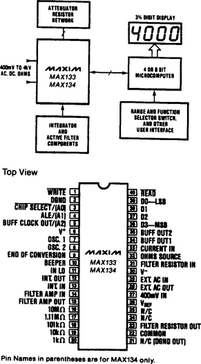
FIGURE 10-1 Typical operating circuit and pin configuration (Maxim Evaluation Kit Data Book, 1994, p. 4-79)
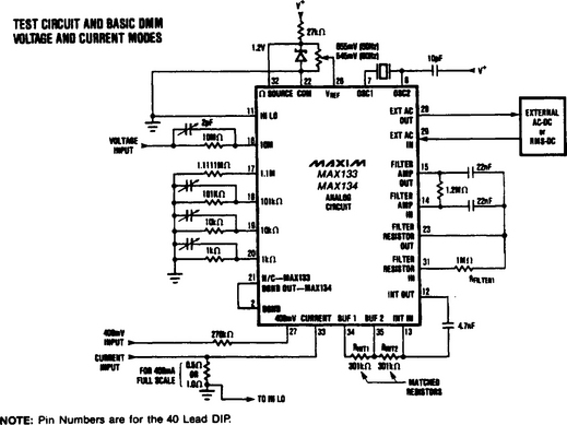

FIGURE 10-3 Coordination of MAX133/134 and microprocessor (Maxim Evaluation Kit Data Book, 1994, p. 4-82)
The MAX133/134 contains an ADC and auxiliary circuitry such as attenuator range switches, a piezoelectric beeper driver, an active filter, a low-battery detector, and both analog and digital power supplies, but it does not include any display-drive capability. The IC reduces component count and system cost by minimizing the external components required for the analog portion of the system, but it does not restrict final production features by including autoranging or other digital-control functions.
The IC is intended to work as the analog front end of a microprocessor; the features of the end product are determined by microprocessor software. The IC provides all the logic and counters for control of the conversion sequence, and the microprocessor does not perform any critical timing of complex control of the IC.
The IC has three range switches for a five-decade attenuator (which uses external resistors) and has additional mode-selection circuits for performing voltage, current, AC or DC, ohms, and continuity measurements. The five-decade attenuator and mode-selection circuits are controlled by the microprocessor through control bits written into the IC.
Figure 10-4 shows the basic elements of the input section. This includes the A/D (analog-to-digital converter), input range switching, and several control circuits.

The IC has a typical mode rejection of the line frequency of at least 80 dB on the voltage ranges; the microprocessor selects rejection of either 50 Hz or 60 Hz by setting a control bit on the IC. A two-pole active filter can also be turned on by the microprocessor, adding about 40 dB normal mode rejection above 50 Hz.
The basic blocks of the MAX133/134 are as follows:
Each of these blocks or sections is discussed in the following paragraphs.
10.1.1 A/D Section
The A/D (or ADC) uses a “residue-multiplication” conversion scheme to provide a full ±40,000-count-resolution reading every 50 ms. This is done with the good noise performance and power-line normal-mode rejection associated with integrating ADCs (see Section 10.4 for a description of the conversion method).
All timing and ADC-conversion phase control is performed by the IC without microprocessor intervention. The A/D section performs a non-zero-corrected conversion every 50 ms (20 conversions per second).
The microprocessor must periodically direct the IC to perform a read-zero conversion, which also takes 50 ms. This read-zero conversion is performed with IN LO (low input) internally shorted to IN HI (high input), and the result of zero conversion must be subtracted (by the microprocessor) from normal measurements to provide a zero-corrected reading.
The zero correction that must be subtracted is determined by the MAX133/134 internal offsets. Because these offsets are relatively slow changing, zero conversion readings need only be taken often enough to track long-term drifts and temperature changes. The zero-conversion reading changes slightly with a change in common-mode input voltage or reference voltage, and a new zero-conversion reading should be taken if either of these changes.
In ratiometric ohms measurement, the reference voltage changes considerably as the value of the unknown resistor varies. To reduce the errors caused by the system offset, the IC “chops” the input buffer and integrator. This “chop” consists of a reversal of the input transistors during the conversion cycle. The timing of the chop is such that in the R/2 or ohms-measurement mode, the system offset is almost completely nulled out if the X2 mode is not selected. Even if the X2 mode is selected, the system offset does not exceed 5,000 counts on any range. Because the internal full-scale range is greater than ±49,000 counts, at least ±40,000 counts of resolution are available after zero-offset correction.
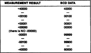
Each conversion result is latched into a conversion register that can be read by the microprocessor. The data format is nines-complement BCD (a zero reading is 00000, a−1 reading is 99999, a −25000 reading is 75000). The nines-complement form is the most convenient BCD format because the addition of the nines-complement of a number is equivalent to subtracting that number (see Section 10.6 for BCD-to-binary conversion).
The last digit of conversion is used for digital autozero and is usually not displayed. Each count of the least-significant digit of the IC output corresponds to Vio of a count, if a 4,000-count full-scale display is used.
For current ranges with a voltage drop of only 200 mV, the measured reading can be multiplied by two, using the X2 function. The X2 function reduces the RINT resistor value by a factor of two during the integrate phase. With the X2 range, a 200-mV input results in a full-scale 4.000.0 measured reading.
As an alternative, the normal 400-mV range can be used, with the multiplication by two being done (digitally) by the microprocessor. In this case, each count of the least significant digit is 1/5 of the displayed count. A 100-mV full-scale voltage drop can be achieved using both the X2 range and digital times-two multiplication in the microprocessor.
Each of the 20 conversions per second has a zero-integrator phase to ensure rapid recovery from overload. The IC recovers (to within two counts) one conversion time after an overload of 10 times full scale (when the onboard active filter is not used, see Section 10.1.4).
10.1.2 Input Range Switching
In voltage-measurement ranges other than 400 mV, voltages are applied to the 10-M pin through an external 10-M resistor as shown in Fig. 10-2. With selection of the proper shunt resistance (1.1 M through 1 k), the input voltage is attenuated to 400-mV. The input-attenuator switch section includes analog switches to switch the input current and to sense the voltage on the shunt resistor. Other input-switching functions select between the input-attenuator output and the voltage developed across the current-sensing resistors during measurement.
The 5-pA input-bias current might result in unacceptable errors with a 10-M input resistor on the 400-mV scale, so a separate pin with a 100-k to 1-M input resistor is used. The 10-M resistor used on the higher voltage ranges does not cause appreciable error because the input-leakage current is shunted to ground through the 1.11-M to 1-k attenuator shunt resistors.
To avoid errors that might occur through high-frequency coupling, high-voltage signals from the attenuator input to the 400-mV and current inputs have 10-k switches which connect the inputs to ground when not selected. The input section also includes switches for an external AC-DC converter to be inserted into the signal path (see Section 10.5.3).
10.1.3 Ohms and Diode Measurement
Figure 10-5 shows the basic connections for ohms (resistance) measurement and diode test. The input-attenuator resistors are also used in the ohms mode. (The 10-M resistor must be externally paralleled with other resistors to obtain exactly 1 M, 100 k, etc.) The ohms buffer input (OHMS SOURCE, see Fig. 10-4) is usually connected directly to an external reference or to another 1.25-V source.
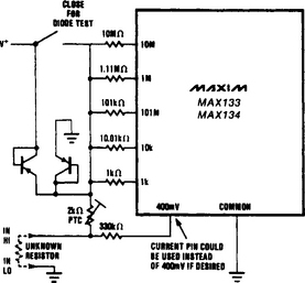
FIGURE 10-5 Basic connections for ohms and diode test (Maxim Evaluation Kit Data Book, 1994, p. 4-85)
In the 4-k through 40-M ranges, there is a total of 1.25-V across the series combination of reference resistor, unknown resistor, and the input-protection network. The maximum voltage across the unknown resistor at full-scale is less than 400 mV. On the 400-ohm range, the ohms voltage source is a diode connected to V+ through a 2-k p-channel switch. With a 3-V common voltage, this supplies about 2.2 V across the series combination of reference resistor, unknown resistor, and input-protection network. This higher voltage is used on the 400-ohm range to compensate for the decrease in reference voltage caused by the input-protection network. The IC operates with PTC (positive temperature coefficient) protection resistors of 2 k or less.
The voltage across the reference resistor is used as the reference voltage for the A/D in the ohms mode. The differential voltage between IN LO and IN HI is the input signal. The integration period is 500 counts independent of the 50/60-Hz control-bit setting.
The digital output code is as follows:
with a maximum non-zero-corrected output code of ±49,500 and a maximum zero reading of 5,000.
A 1-k reference resistor is used for the 400-ohm full scale, a 10-k reference for a 4-k full scale, and so on. A 10-M reference resistor is used for both the 4-M full scale and the 40-M full scale. To obtain the correct results in the ohms-measurement or R/2 mode, the conversion result must be multiplied by two. This can be done digitally by the microprocessor or by the X2 range except on the 40-M scale. The 40-M range has the same reference resistor as the 4-M range, but a times-10 scale factor is obtained by not multiplying by 2 and by activating the divide-by-5 function.
If the times-five multiplication is performed by the microprocessor, the read-zero offset of the IC in the ohms mode is just a few counts and is nearly independent of the unknown-resistor value. If the X2 mode is used to multiply by 2, then frequent read-zero readings should be taken, because the read-zero offset is inversely proportional to the reference voltage (which varies as the unknown resistor varies).
Because the input-protection resistor shown in Fig. 10-5 reduces the reference and input voltage, particularly on the 400-ohm scale, the PTC resistance should be as low as possible but still must maintain the desired level of protection. A PTC resistance in excess of 2 k increases the noise level for measurements on the 400-ohm range.
Because the IC does not use a reference capacitor, the only limit on the response time in the ohms mode is the active filter. Even when the active filter is turned off, RFILTER1 (see Fig. 10-4) is still connected, and the input voltage must charge the filter capacitors. This generally is noticed only on the 4-M and 40-M ranges.
A diode-test range can be implemented by connecting the PTC (used for input protection in the ohms ranges, see Fig. 10-5) to V+. The PTC then delivers about 1 mA of current to the diode (connected between IN HI and IN LO). The diode voltage can be measured on the standard 4-V scale, or on the 400-mV scale with the divide-by-five function activated to result in a 2-V full scale. As always, the latched-continuity circuit is active, and latches whenever the input voltage goes below about 100 mV. The microprocessor can also test the measured voltage at the end of each conversion, if a more precise detection of continuity threshold is desired.
10.1.4 Active Filter
Figure 10-6 shows the basic connections for the active filter. (Figure 10-4 shows connections to the input section of this two-pole filter.) The op-amp offset has no effect on the DC accuracy because the op amp is AC coupled (only), and the DC signal path is through the passive 1-M resistor.

The active filter limits the response time or speed to input-voltage changes. For that reason, it might be desirable to disconnect the input voltage during autoranging. Because the source impedance at the filter input varies with the input attenuator selected, the response time is slower on the 4-V range.
10.1.5 Oscillator and Beeper Driver
The IC is designed to operate with a 32768-Hz tuning-fork crystal similar to the Statek CX-IV; only one external capacitor and no external resistors are used. If desired, the OSC1 pin can be driven externally.
The 32-kHz clock is used internally as the clock for the sequence and measurement counters. The clock is also divided down to 2,048 Hz and 4,096 Hz to drive a beeper. The beeper output swings from V+ to V–, and can directly drive piezoelectric beepers.
Two control bits set by the microprocessor select the frequency (2,048 or 4,096 Hz) of the beeper and turn on and turn off the beeper. The beeper is controlled by the microprocessor and can be used for both continuity indication and an audible operator-feedback signal to indicate peak-hold or range changes.
10.1.6 Power Supply and Low-Battery Detector
Although the ICs are designed to operate with a 9-V battery, ±5-V supplies also can be used. The maximum supply current is 250 μA, with a typical operating current of 100 μA. An on-board low-battery detector indicates when the battery voltage is approaching the minimum operating voltage of about 6.8 V.
As shown in Fig. 10-2, analog common (COM) is taken from a zener and is nominally 3.0 V less than V+. For low-cost applications, the common voltage (with a temperature coefficient, or tempco, of 80 ppm/°C) can be used as a reference. However, in most applications, a bandgap reference is connected to common, with a pullup resistor to V+. A voltage divider connected across the bandgap reference generates the 545-mV (60-Hz operation) or 655-mV (50-Hz operation) reference voltage applied to Vref. In a battery-powered meter, the COM pin is used as the system ground-reference point.
The IC can also generate a digital-ground voltage, which is nominally 5-V below V+. This voltage remains in the range of 5 V ± 10%, with a sink capability of 5 μA to 500 μA. The DGND (digital ground) generator has substantial current-sinking capability but can easily be pulled to a more negative voltage because the current-sourcing capability is only 1 μA typical.
The MAX133 internally connects the digital-ground generator to the DGND pin (see Fig. 10-2). Normally, the MAX133 is powered by a 9-V battery, and the ground, V-, or VSS pin of the microprocessor is connected to the MAX133 DGND pin.
The MAX134 connects the DGND voltage generator to the DGND OUT pin. (The MAX134 DGND pin is an input only.) When the MAX134 is used with a 9-V battery, connect the DGND OUT pin to the DGND pin. For use with ± 5-V supplies, connect the DGND pin to ground, V+ to +5V, and V– to−5 V.
10.2 Digital Interface
The MAX133 and MAX134 differ only in their digital interface. The MAX133 has a multiplexed address and bidirectional data bus. The MAX134 has three separate address lines in addition to a bidirectional data bus. In both ICs, the data bus has 4 bits. This permits use of both ICs with 4-bit or 8-bit microprocessors.
10.2.1 MAX134 Digital Interface
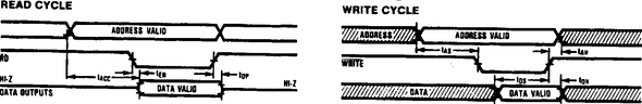
Figure 10-7 shows the read-write sequence between the MAX134 and the microprocessor. A 4-bit bidirectional bus, D0-D3, is required for interface. In addition to the four data-bus lines, there are three address lines (A0-A2), and two control signals—WR (write) and RD (read).
The A0-A2 address lines select one of five control registers. When WR goes low, data bits are written from the bus into the MAX134 control register, addressed by A0-A2. When RD is low, the MAX134 drives the bidirectional bus. The data bits contained in the results or status register (and addressed by A0-A2) are placed on the bus.
10.2.2 MAX133 Digital Interface
Figure 10-8 shows the read/write sequence between the MAX133 and the microprocessor. Only seven lines are required for this interface. The microprocessor first selects the register to be read or written to by placing the register address onto a 4-bit multiplexed address-data bus. The microprocessor then pulses the address latch enable (ALE) line high to latch the register address into the MAX133.
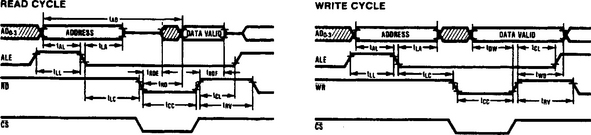
To read the selected register, the microprocessor drives the read line low, and the MAX133 places the register data onto the data bus. To write to the selected register, the address is latched as described, then the microprocessor places the data onto the bus. When this is complete, the microprocessor pulls the write line low. The MAX133 latches the data into the selected register on the rising edge of write. The chip-select (CS) line must be low to enable either the RD or WR lines, but ALE is not gated by CS.
10.2.3 MAX133/134 Digital Interface
In most cases, the EOC (end of conversion) signal is either monitored by an I/O pin or drives an interrupt to the microprocessor. In battery-powered systems, it might be desirable to put the microprocessor in a standby mode until EOC goes high. The microprocessor can then perform any required data-processing and display updates and then return to standby. This conserves battery power because the microprocessor power consumption is minimized.
The data bits that have been latched in the MAX133/134 control registers do not immediately affect operation. The input registers are double buffered, and the control bits take effect during the 21st clock cycle after EOC goes high. In the hold mode, the double-buffered registers are transparent, and any updates to the registers take effect immediately, as do any changes made during the one-clock-cycle period at the end of each conversion. (This is the time during which the second rank of buffers are being updated.)
10.2.4 Description of Output Bits
Figure 10-9 shows examples of the nines-complement BCD format used for data output. In addition to data, the latched-continuity output bit is high if the input voltage goes below the continuity threshold of about 100 mV since the last time the register was read. Each time this register (register 5) is read, the continuity latch is reset. The low-battery output bit is high whenever the battery voltage is less than the low-battery detect voltage (about 6.8 V). The holding output bit is low whenever the MAX133/134 is in the hold state.
10.2.5 Description of Control Bits
Figure 10-10 shows the register map of output data from the MAX133/134 to the microprocessor. Figure 10-11 shows the same information for input data from the microprocessor. The following is a summary of the bit functions.
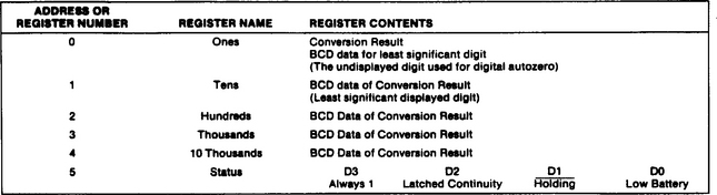
FIGURE 10-10 Register map of output data to microprocessor (Maxim Evaluation Kit Data Book, 1994, p. 4-87)
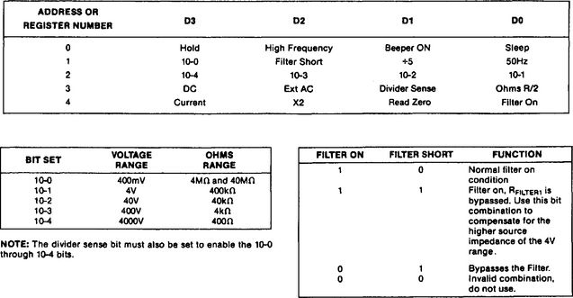
FIGURE 10-11 Register map of input data from microprocessor (Maxim Evaluation Kit Data Book, 1994, p. 4-88)
Hold.
A 1 in hold stops conversions at the end of the next conversion. If the MAX133/134 is in the hold mode, a conversion starts on the next clock cycle after hold is set to 0. The oscillator continues to run and all circuitry is active during the hold mode.
High Frequency.
A 1 in the high-frequency bit selects 4,096 Hz as the beeper frequency. A 0 selects 2,048 Hz.
Sleep.
A 1 in sleep puts the MAX133/134 into the sleep or standby mode. The common voltage buffer is turned off, as is the internal analog circuit, but the DGND circuit is still active. The oscillator continues to run. Current consumption is reduced to 25 μA. Several conversions must be performed after one exits the sleep mode before full conversion accuracy is obtained.
10-0 through 10-4.
These bits control the attenuator-network switches. The 10-0 bit selects the 10-M input without activating any shunt resistors. This is an alternative 400-mV input. The 10-1 bit activates the 10:1 attenuation by selecting the 10-M input and connecting the 1.111-M shunt. Similarly, 10-2, 10-3, and 10-4 bits select input attenuation factors of 100, 1,000, and 10,000, respectively. In the ohms mode, these bits set the resistance range.
50Hz.
When set to 1, the integration period for voltage measurements is one cycle of the 50-Hz power mains (655 clock cycles). When 0, the integration period is one 60-Hz power-line cycle (545 clock cycles).
×2.
Setting the bit to 1 activates the “times-2” function. When X2 is active, RINT2 only is used as the integrator resistor during the integration phase. RINT1 and RINT2 in series are used as the integration phase when X2 is 0. If RINT1 = RINT2, setting the X2 bit doubles the digital output for a given input voltage.
÷ 5.
When this bit is set to 1, the integration period is reduced by a factor of 5. This reduces the digital-output code by a factor of 5 and allows a higher input voltage to be used. The full-scale input voltage is multiplied by 5 when this bit is set. Caution should be used to make sure that the 2-μA maximum recommended integrator output current is not exceeded, resulting in degraded linearity.
Ohms or R/2.
Setting this bit to 1 selects the ohms measurement mode (see Section 10.1.3). Set the divider sense to 0 for ohms measurement.
Read Zero.
Setting this bit to 1 causes the next conversion to be a read-zero conversion. The IN HI and IN LO terminals are shorted internally during a read zero. The reference selected by the other control bits is used. The read-zero conversion result is proportional to the internal offsets of the MAX133/134. This result should be subtracted from other measurements to obtain zero-corrected readings.
DC.
This bit selects the DC mode when set to 1 and selects AC when set to 0. The bit should also be set for ohms measurement.
10.3 Component Selection
Observe the following notes when selecting components for the single-chip DMM.
10.3.1 Integration Resistors
For an accurate times-2 multiplication in the X2 mode, the two RINT resistors (see Fig. 10-2) must be equal. If the X2 mode is not needed, connect a 604-k RINT1 between BUF OUT 1 and the 4.7-nF integration capacitor. Leave BUF OUT 2 open. The value of both RINT1 and RINT2 is normally 301 k for a 545-mV or 655-mV reference. This sets the integrator output current to 2 μA during the deintegrate phase. Do not exceed 8-μA integrator current.
10.3.2 Integration Capacitor
The nominal value for the integration capacitor is 4.7 nF. This value, in combination with the integrator output current and the clock frequency, sets the integrator swing to about 3 V for the voltage ranges when RINT1 = RINT2 = 301 k, and the clock frequency is 32,768 Hz.
Although this same integrator swing can be obtained with other capacitor values by changing the value of RINT, lower values of CINT might introduce more noise through increased noise pickup and 50/60-Hz signals. Excessively high values of CINT also cause noise problems by reducing the integrator swing to unacceptably low values, causing the comparator noise to dominate the conversion errors. Large values of CINT also cause linearity errors because the settling time of the internal times-10 circuits is affected by the value of CINT.
The dielectric absorption of the integration capacitor directly affects the integral linearity. High-quality polypropylene capacitors are recommended. Polycarbonate and polystyrene capacitors might give satisfactory performance in less demanding applications. Polyester (Mylar) capacitors cause about 0.1% integral nonlinearity.
10.3.3 Active Filter
The RC time constant of the active-filter components shown in Fig. 10-6 sets the rolloff frequency. The effective value of RFILTER1 is the sum of its value plus the source impedance driving the filter. For example, at 30 V, the effective source impedance is the 101-k resistor in the attenuator. At 3 V, the effective source impedance is 1 M. This variable source impedance alters the filter characteristics somewhat as the different voltage ranges are selected.
The effect of the different source impedances can be minimized by increasing the value of the filter resistors and decreasing the filter-capacitor values in proportion. However, this increases the offset error caused by the A/D input-leakage current flowing through the filter resistors. For simplified design, use filter-resistor values between 1 M and 3 M.
A low rolloff frequency improves the normal mode rejection but at the expense of a longer settling time in response to input-voltage step changes. Aliasing is another consideration, particularly when an LCD bar graph is used with the DMM. If the bar graph is updated at 20 times per second and there is a 19-Hz component in the signal being measured, the beat frequency of 1 Hz appears on the LCD bar-graph display. To avoid aliasing effects, the filter time-constant is normally set less than 10 Hz. A 3-Hz rolloff (RC = 40 ms) further reduces the aliasing effects and increases normal mode rejection but still maintains an acceptable transient response with fast-varying signals.
As in the case of the integration capacitor, polypropylene capacitors are recommended. This is because dielectric absorption in the filter capacitors creates a small (but significant) time-constant settling error.
10.3.4 Crystal Oscillator
The oscillator is designed to use high-Q, low-power 32, 786-Hz crystals such as the Statek CX-IV. The series resistance should be less than 30 k. The oscillator capacitor connected to OSC2 (see Fig. 10-2) is typically 10 pF but should be adjusted to optimize performance with the chosen crystal. If overtone oscillations are observed, increase the value of the oscillator capacitor. Decrease (or eliminate) the capacitor if the oscillator has start-up problems. Keep stray capacitance across the crystal to a minimum. Such stray capacitance might prevent oscillation.
10.3.5 Attenuator Network
Figure 10-4 shows the attenuator network and the associated range-selection switches. If the resistance of the internal range-selection switches is 0 ohms, the theoretical values for the attenuator are 10 M, 1.1111 M, 101.101 k, 10.01 k, and 1.000 k. However, the important point to remember is that the resistors must track each other. This is because the ratio of resistor values sets the accuracy of the voltage measurements. As always, the temperature coefficients of the various attenuator resistors should be as low as practical. The voltage coefficient of the 10-M resistor should also be low because this resistor has high voltages applied (in the 400-V and 4,000-V ranges).
10.3.6 Attenuator Compensation Capacitors
The input attenuator is often compensated with low-value capacitors (see Fig. 10-2). These capacitors maintain a constant attenuation ratio over a wide bandwidth. Keep the capacitor values low to prevent the 10-M pin from being driven above V+ or below V– when high-frequency, high-voltage signals are applied. Such a condition can cause gross conversion errors.
10.3.7 PTC Resistor
As shown in Fig. 10-5, an adjustable PTC resistance is normally used as part of the protection circuit in the ohms mode. Excessive values of PTC resistance can reduce the voltage across the unknown and reference resistors, particularly at 400 ohms. PTC resistances greater than 2 k degrade system performance by reducing the signal level at 400 ohms, increasing the conversion noise. Values greater than 5 k cause additional error because the voltage drop across the PTC appears at the ADC as a common-mode difference between IN HI and IN LO.
10.3.8 Microprocessors
For low-cost two-chip digital multimeters, Maxim recommends 4-bit microprocessors with LCD display drive capability. Typical 4-bit microprocessor families include the Sharp SM4 and SM5, the NEC mPD75XX family, and the Hitachi LCD-Ill and LCD-IV families. If additional calculation power is needed, or if software development costs and time must be minimized, then 8-bit microcontrollers such as the 8048, 8051, or 6803 should be used.
10.4 Conversion Method
Figures 10-12, 10-13, and 10-14 show typical integrator and buffer waveforms for a large-positive, a large-negative, and a small-positive input voltage, respectively.


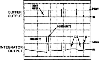
The following is a summary of the “residue multiplication” technique used to perform a ±40,000-count conversion in 1,638 clock cycles.
10.4.1 Integration Phase
Figure 10-15 shows the integration periods for the various modes of operation. Figure 10-16 shows the basic elements of the ADC analog circuits. The unknown signal is integrated by connecting the noninverting input of the integrator to IN LO and the buffer input to IN HI. The integration period varies from 100 counts to 655 counts, as shown in Fig. 10-15. The IC is in the zero-integration phase while in hold (between conversions) and before the start of the integration period.
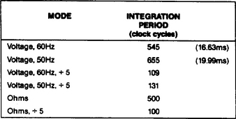
FIGURE 10-15 Integration periods for operating modes (Maxim Evaluation Kit Data Book, 1994, p. 4-90)

Digital output code = Integration period × 100 × Vin/Vref
where Vin is the differential voltage applied to the ADC internal IN HI and IN HO and Vref is the differential voltage applied to the ADC internal REF HI and REF LO shown in Fig. 10-16.
10.4.2 First Deintegration Phase
The polarity of the first deintegration phase is determined by polarity of the voltage on the integration capacitor CINT at the end of the integration period. No reference capacitor is needed, improving the response time in ohms measurement. Also because the noninverting input of the integrator is connected to REF HI for a positive deintegration, the voltage at the integrator output has a step voltage-change equal to the reference voltage.
The first deintegration phase terminates when the comparator detects that CINT has been discharged. The IC then goes into an “idle” state in which both the buffer input and the noninverting input of the integrator are connected to common. This causes the system offset to be integrated. Near the end of the maximum allowable deintegration period, the polarity of the voltage on CINT is again tested, and either a positive or negative deintegration cycle occurs.
10.4.3 Times-10 (X10) Phase
When zero-crossing is detected at the end of a deintegration phase, the deintegration is continued until the next clock cycle. This causes the integrator to overshoot zero-crossing slightly, leaving a small residual voltage on CINT. Any comparator delay causes an additional residual voltage on CINT. The times-10 phase inverts and multiplies this residual by a factor of 10.
10.4.4 Second Deintegration Phase
The second deintegration phase deintegrates the residual voltage on CINT. (This voltage has been inverted and multiplied by 10 during the X10 phase.) Because the voltage across CINT is multiplied by 10, each clock cycle during second deintegration corresponds to Vio of one clock cycle during the first deintegration phase.
10.4.5 Second X10 and Third Deintegration
The residual voltage on CINT after the second deintegration phase is multiplied by the second X10 phase, and this multiplied residual is deintegrated in the third deintegration phase. Because the residual voltage on CINT has been multiplied twice by 10, the third deintegration phase has 100 times finer resolution than does the first deintegration phase.
10.4.6 Sequence Counter and Results Counter
The sequencing or timing of the various conversion phases is controlled by a binary sequence counter. This counter counts upward continuously except during the hold mode. Some phases, such as the integration periods, are both started and stopped at present counts. The deintegration phases are started at predetermined counts but are terminated when the comparator detects zero-crossing at the integrator output.
The results counter accumulates counts during all deintegration phases. It is an up-down BCD counter, the count direction being determined by the deintegration polarity. The first deintegration phase causes the results counter to count by hundreds. Because the second deintegration phase is deintegrating a residual voltage that has been multiplied by 10, the results counter is incremented or decremented by ones during the third deintegration phase. The contents of the results counter are transferred to the results register at the end of each conversion.
10.5 Application Notes
The following manufacturer’s recommendations should be considered when using the MAX133/134 for any application.
10.5.1 Sleep and Hold Modes
The hold mode stops the internal sequence counter at the end of the next conversion, but does not turn off the oscillator or any analog circuit. The hold mode can be used to accelerate autoranging (see Section 10.6.1). Dielectric absorption in CINT causes the first two or three readings after an extended hold period to have a lower magnitude than the steady-state reading.
The sleep mode puts the IC into a low-power quiescent mode by shuting off all analog circuits except the DGND power supply and the oscillator. A typical use for the sleep mode is to reduce power consumption by turning off the IC if the meter is idle for a long period. A typical method of detecting when the meter is no longer being used is to detect when the reading stays constant and there are no operator inputs (such as range or mode changes) for an extended period.
Because the sleep mode turns off all analog circuits, the first conversion after coming out of the sleep mode is not valid. It takes several readings before the reading has stabilized to within one count.
10.5.2 Input Protection for Digital Multimeters
Figure 10-5 shows a typical multimeter input circuit for ohms measurement. The adjustable PTC resistor (actually a thermistor) normally has a resistance of 2 k. However, under overload conditions, the PTC limits current because the current heats the PTC, drastically increasing the resistance.
Protection on the voltage ranges is automatic, because the 10-M input resistor limits the input current to safe limits, even with 4,000 V applied. The current ranges must be protected with fuses or circuit breakers. Current-sense resistors should be bypassed with diodes. As a simplified-design guide, voltage drop across the current-sense resistors should be limited to no more than two diode drops (typically about 1 V).
10.5.3 External AC-DC Converter
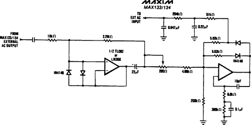
Figure 10-17 shows a half-wave external AC-DC converter. The circuit is an average-sensing, RMS-calibrated converter. This means that the output is proportional to the average AC value, rather than RMS value, but that the output is multiplied by 1.11 to correct for the ratio of average voltage to RMS voltage in a sine wave. If desired, a true RMS to DC converter can be used instead. Such a converter must be connected between the EXT AC IN and EXT AC OUT pins (in place of the Fig. 10-17 circuit).
10.5.4 PC Board Layout
Because the integrator output makes common-mode voltage steps equal to reference voltage (to perform a positive deintegration), any stray capacitance on CINT causes errors. Stray capacitive loading on the buffer output should be minimized to avoid ringing at the buffer output. The integrator-in node is particularly sensitive to stray pickup of noise and 50/60-Hz line noise, so keep CINT close to the INT IN pin.
Minimize capacitance on the node that joins the two RINT resistors. This capacitance sets up an RC time constant that rounds off the edges of the comparator input and can cause errors. If the times-2 mode is not used, connect a single RINT1 resistor directly from BUFF OUT 1 to the INT IN pin. Locate RINT1 as closely as possible to the INT IN pin (because the buffer output is a low-impedance point and INT IN is high impedance).
Any resistance between the 1-k pin and the 1-k resistor adds to the effective value of the 1-k resistor. This is also true of any voltage drop between the 1-k resistor and the IN LO pin. These resistances should be minimized or the 1-k resistor value should be reduced to compensate for the resistance of the PC board connections.
The effective resistance of any current-sensing resistors is affected by where the voltage is sensed. Connect IN LO directly to one end of the current-sensing resistor to avoid errors caused by voltage drops in the common traces on the PC board.
10.6 Software Notes
The following manufacturer’s recommendations should be considered when configuring the MAX133/134 and microprocessor software.
10.6.1 Autoranging
Figures 10-18 and 10-19 show the autoranging sequence when the IC is running continuously and when there is a hold between conversions, respectively. The sequence in which the registers are loaded has no effect, provided that all registers are loaded before the next EOC. Control bits take effect only when the IC is in hold or when the current conversion is completed.
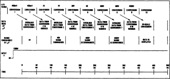
FIGURE 10-18 Autoranging sequence for continuous run (Maxim Evaluation Kit Data Book, 1994, p. 4-93)
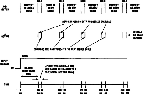
FIGURE 10-19 Autoranging sequence with hold between conversions (Maxim Evaluation Kit Data Book, 1994, p. 4-93)
If the IC runs continuously, the autoranging sequence is as shown in Fig. 10-18. If the IC is put into the hold mode during autoranging, the autoranging time can be reduced when several ranges must be tried. This is shown in Fig. 10-19.
A simple test that detects most overrange readings is to check if the two most significant bits (registers 3 and 4) are greater than ±45. A second test of the zero-corrected reading should be performed to make sure the reading is within the desired full-scale range.
10.6.2 Reducing Conversion Noise
The MAX133/134 has about ±1 counts of noise. In most cases, where only 4,000 counts are being displayed, averaging is not required because the noise is only 1/10 of one displayed count. In data-acquisition systems (see Section 10.7) in which the full resolution is being used, averaging N readings reduces the noise by a factor equal to the square root of N. Thus if 50 readings are averaged, the noise is reduced by a factor of just over 7.
Because the noise of zero-corrected readings is the RMS sum of the noise of both the read-zero reading and the normal reading, the read-zero offset (see Section 10.2.5) should be averaged for best noise performance.
10.6.3 BCD to Binary Conversion
Normally, if only a zero correction or tare correction is to be applied to the IC output, the conversion result is left in BCD. If a scale factor or gain correction must be made, the result is usually converted to binary. Any of the standard BCD-to-binary conversion algorithms can be used.
A simple method of conversion is to read the MAX133/134 conversion result, starting with the most significant bit. Put the result into a multibyte accumulator and multiply the result by 10. Then read the result for the next digit and add that to the accumulator. Repeat the “multiply-read-add” sequence for all five digits.
10.7 Using the IC in Data-Acquisition Systems
The following manufacturer’s recommendations should be considered when using the MAX133/134 for data-acquisition systems.
10.7.1 Using the Input Attenuator as a Multiplexer
Figure 10-20 shows how the input section can be used as a multiplexer. This is suitable for data-acquisition systems in which the voltage range is limited, and the 400-mV to 4,000-V attenuators are not needed.

10.7.2 Using Nonstandard Voltage Ranges
In many data-acquisition systems, the voltage to be measured might have a full-scale range other than 400 mV, 4 V, and so on. For maximum resolution, the full-scale range should be adjusted to match the input-signal voltage span. This can be done either through attenuation or amplification of the signal (to make the signal match the basic ±400-mV span of the MAX133/134) or by means of adjusting the IC voltage span.
Figure 10-15 shows the integration periods of the various conversion modes. These different modes can be used to change the full-scale span of the IC. For example, if the reference voltage is 545 mV, setting the 50-Hz bit changes the integration time to 655 clock cycles, and the 400-mV full-scale range becomes a 545/655 × 400 mV = 333-mV full-scale range.
Activating the ÷ 5 bit increases the full-scale span by a factor of 5. Setting the X2 bit decreases the full-scale span by a factor of 2 (assuming that RINT1 = RINT2).
In all cases, the values of RINT1, RINT2, and CINT should be chosen so that the integrator swing is at least 2 V, and integrator current is always less than 3 μA, during both deintegration and integration with a full-scale voltage. The common-mode voltage range of IN HI and IN LO is (V– +1.5 V) to (V+ −1.0 V).
10.7.3 Unipolar Operation
Unlike many integrating ADCs, the MAX133/134 does not have extra nonlinearities when the reading is near zero. This makes it possible to use the full 80,000-count resolution to measure unipolar signals. All that is needed is a resistive offset network to translate the unipolar signal so that it becomes bipolar. An external zero circuit must be included so that errors in the offset resistor can be measured and subtracted. The zero-correction software is the same as would be used to correct for the internal zero error of the IC, except that in this case the external zero offset is nearly 40,000 counts.
10.7.4 Ratiometric Measurements
Ratiometric measurements (see Section 3.2.1) are used in many weigh-scale, pressure-transducer, and load-cell applications. If the reference voltage is referenced to ground or the common pin, simply connect the reference voltage to IN HI and IN LO, and perform any of the voltage-mode conversions.
When the reference voltage is a differential signal, use the circuit of Fig. 10-21. The programming table for Fig. 10-21 is given in Fig. 10-22. Use the bit pattern on Fig. 10-21 to select the ohms measurement mode.
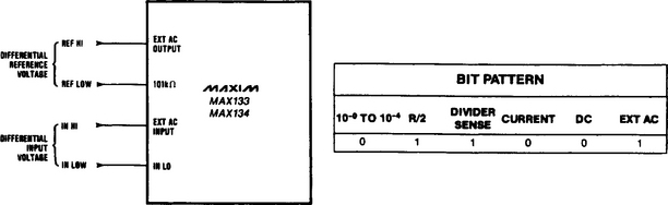
FIGURE 10-21 Configuration for differential reference input (Maxim Evaluation Kit Data Book, 1994, p.4-95)

FIGURE 10-22 Programming table for differential reference input (Maxim Evaluation Kit Data Book, 1994, p. 4-94)
The noninverting input of the integrator is connected to either REF LO or REF HI during deintegration. The integrator swing should be reduced if the integrator output goes within 0.5 V of either V+ or V−. In no case should either REF HI or REF LO be lower than (V− +1.5 V) or higher than (V+ −1.0 V).
10.7.5 Operation at Other Clock Frequencies
Noise performance can be improved when operating with clock frequencies lower than 32 kHz. However, the reading rate is reduced in proportion. With clock frequencies less than 10 kHz, leakage during the X10 phase introduces differential linearity errors at high temperatures.
Clock frequencies higher than 50 kHz are not recommended because the X10 period will not completely settle within the allotted time period, causing differential nonlinearity errors. Another potential problem at very high clock frequencies is that although the comparator delay is a fixed time period, the delay increases in terms of clock cycles as clock frequency increases. At very high clock frequencies, the residue cannot be fully deintegrated in the allotted number of clock cycles after having been multiplied by 10 in the X10 phase. When using a clock frequency other than 32,768 Hz, change the value of CINT to keep integrator swing at about 2 V.
10.7.6 Converting X2 to ± 40-mV Full-Scale
The sensitivity of the X2 mode is increased by the factor
In the normal DMM application, RINT1 = RINT2 and the X2 mode increases the sensitivity of the IC by a factor of 2. If the two resistors have a 9:1 ratio, the X2 bit increases the sensitivity by a factor of 10. This can be used to get l-μV resolution on a 40-mV scale.
10.7.7 Disabling the Active Filter
Because the source impedance in many data-acquisition systems is very low, the value of the filter resistors (RFILTER1 and RFILTER2) can be lowered to reduce the error caused by the ADC leakage current flowing through the resistors. If rapid settling is needed in a multichannel data-acquistion system, then the filter should be disabled. This is done by leaving the FILTER RESISTOR IN and FILTER RESISTOR OUT pins open and shorting the FILTER AMP OUT to FILTER AMP IN. However, do not leave the filter-amplifier connections open circuited. This can result in oscillation.