Data-Converter Terms and Design Characteristics
Much of the basic design information for a particular IC data converter can be obtained from the data sheet. Likewise, a typical data sheet describes a few specific applications for the data converter. However, converter data sheets often have two weak points. First, they assume that everyone understands all the terms used. Of more importance, the data sheets do not show how the listed parameters relate to design problems. To further complicate the situation, each manufacturer has a separate system of data sheets. It is impractical to discuss all data sheets herein. Instead, we discuss typical information found on the converter data sheets, and see how this information affects simplified design. We start with definitions of some basic terms.
2.1 Resolution and Accuracy
The terms resolution and accuracy are often interchanged (although incorrectly). In a DAC, resolution describes the smallest standard incremental change in output voltage. In an ADC, resolution is the amount of input voltage change required to increment the output between one code change and the next adjacent code change. Both definitions of resolution differ from the definition of accuracy, which is the absolute error incurred in measurement of a signal. In many data converters, accuracy does not match resolution. Let us consider some examples.
A converter with n switches can resolve one part in 2n. The least-significant increment is then 2−n, or one LSB. In contrast, the MSB carries a weight of 2−1. Resolution can be expressed in percentage of full scale, or in binary bits. For example, an ADC with 12-bit resolution can resolve one part in 212 (one part in 4096) or 0.0244% of full scale. A converter with 10 V full scale can resolve a 2.44-mV input change. Likewise, a 12-bit DAC shows an output-voltage change of 0.0244% of full scale when the binary input code is incremented one binary bit (1 LSB). Resolution is a design parameter rather than a performance specification (because resolution says nothing about accuracy or linearity).
A linearity specification (see Section 2.2) is sometimes used in place of accuracy in data converters, because linearity is more descriptive. When used, an accuracy specification describes the worst-case deviation of a DAC output voltage from a straight line drawn between zero and full scale. For example, a 12-bit DAC cannot have a conversion accuracy better than ±½ LSB or ± 1 part in 212+1 (±0.0122% of full scale) because of the finite resolution. This is the case in Fig. 2-1, if there are no other errors. Note that ±0.0122% full scale represents a deviation from 100% accuracy. Therefore, accuracy should be specified as 99.9878%. However, most data sheets would use 0.0122% as an accuracy specification, rather than an inaccuracy (tolerance or error) specification (to further confuse users).
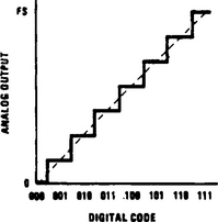
FIGURE 2-1 Linear DAC transfer curve (National Semiconductor, Linear Applications Handbook, 1994, p. 333)
In an ADC, accuracy describes the difference between the actual input voltage and the full-scale weighted equivalent of the binary output code, including all other errors (see Section 2.3). For example, if a 12-bit ADC is said to be ±1 LSB accurate, this is equivalent to ±0.0245%, or twice the minimum possible quantizing error of 0.0122%. In effect, an accuracy specification describes the maximum sum of all errors.
2.2 Linearity
Linearity specifications describe the departure from a linear transfer curve for an ADC or DAC. Linearity error does not include quantizing, offset, zero, or scale errors (see Section 2.3). Thus a specification of ±½ LSB linearity implies error, in addition to the inherent ±½ LSB quantizing or resolution error. This is shown in Fig. 2-2, in which a linearity error allows one or more of the steps to be greater or less than the ideal shown.
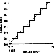
FIGURE 2-2 ADC transfer curve with ½ LSB offset at zero (National Semiconductor, Linear Applications Handbook, 1994, p. 334)
One of the problems with linearity specifications (or nonlinearity specifications, if you prefer) is that there two testing approaches. Figure 2-3 shows how these two approaches (the best-straight-line and endpoint-fit) produce different specifications for an ADC.

FIGURE 2-3 Best-straight-line and endpoint linear curves (Maxim New Releases Data Book, 1992, p. 7-9)
The best-straight-line approach makes no claim about zero error, full-scale error, or transfer-function slope but simply quantifies (in LSBs or percentages) deviation from the straight line that best approximates the transfer function. In effect, the best-straight-line method provides the lowest (or “best looking”) number. No points on the line are defined before the test. The result is a pure linearity specification that includes no other errors.
The endpoint-fit approach presets the ideal line between the measured endpoints of the data-converter transfer function. Deviations are measured without adjusting the position of the line for any optimum fit. As a result, the endpoint-fit linearity number is usually larger than that of the best-straight-line approach. However, both methods are valid ways of representing linearity (also called integral nonlinearity [INL] on some data sheets).
Figure 2-4 shows a 3-bit DAC transfer curve with no more than ±½ LSB nonlinearity, yet one step is of zero amplitude. This is still within the specification, because the maximum deviation from the ideal straight line is ± 1 LSB (½ LSB resolution error, plus ½ LSB nonlinearity).
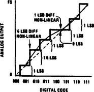
FIGURE 2-4 ±½ LSB nonlinearity curve (National Semiconductor, Linear Applications Handbook, 1994, p. 335)
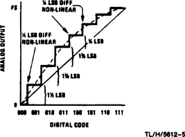
With any linearity error, there is differential nonlinearity (see Section 2.4). A ±½ LSB linearity specification guarantees monotonicity (see Section 2.5) and an equal or better than ±1 LSB differential nonlinearity (DNL). In the example of Fig. 2-4, the code transition from 100 to 101 is the worst possible nonlinearity (1 LSB high at code 100 to 1 LSB low at 110). Any fractional nonlinearity beyond ±½ LSB allows for a nonmonotonic transfer curve. Figure 2-5 shows a typical nonlinear curve, where the nonlinearity is 1 ¼ (LSB), yet the curve is smooth and monotonic.
2.3 Data Converter Errors
The following definitions can be applied to all data converters described in this book, and to virtually all data converters in general.
2.3.1 Quantizing Error
The term quantizing error is usually applied to an ADC. (The equivalent effect in a DAC is more properly called resolution error.) In any case, quantizing error is the maximum deviation from a straight-line transfer function of a perfect ADC. Because an ADC quantizes the analog input into a finite number of output codes, only an ADC with infinite resolution can show zero quantizing error. Figure 2-2 shows the transfer function of such an ADC, suitably offset ½ LSB at zero scale. This transfer function shows ±½ LSB maximum output error. If there were no offset, the error would be ![]() LSB as shown in Fig. 2-6. For example, a perfect 12-bit ADC shows a ±½ LSB error of ±0.0122%, whereas the quantizing error of an 8-bit ADC is ±½ part in 28 or ±0.195% of full scale.
LSB as shown in Fig. 2-6. For example, a perfect 12-bit ADC shows a ±½ LSB error of ±0.0122%, whereas the quantizing error of an 8-bit ADC is ±½ part in 28 or ±0.195% of full scale.

2.3.2 Scale Error
Scale error (also known as full-scale error) is the departure from design output voltage of DAC for a given input code (usually full-scale code). Figure 2-7 shows a transfer function with a linear 1 LSB scale error. In an ADC, scale error is the departure of actual input voltage from design input voltage for a full-scale output code.

FIGURE 2-7 Linear curve with 1 LSB scale error (National Semiconductor, Linear Applications Handbook, 1994, p. 334)
Scale errors can be caused by errors in reference voltage, ladder resistor values, or amplifier gain (see Chapter 1) and can be corrected by means of adjustments in output amplifier gain or reference voltage. For example, if the transfer curve resembles that of Fig. 2-5, a scale adjustment at ¾ scale could improve the overall ± accuracy compared with an adjustment at full scale.
2.3.3 Gain Error
In an ADC, gain error is essentially the same as scale error. In the case of a DAC with current and voltage-mode outputs, the current output can be to scale, but the voltage output might show some gain error. In any case, the amplifier-feedback resistors can be trimmed to correct gain-error problems.
2.3.4 Offset Error
Offset error (also known as zero error) is the output voltage of a DAC, with zero-code input. In an ADC, offset error is the required mean value of input voltage to set a zero-code output. Figure 2-8 shows a DAC transfer curve with ½ LSB offset at zero.

FIGURE 2-8 DAC transfer curve with ½ LSB offset at zero (National Semiconductor, Linear Applications Handbook, 1994, p. 334)
Offset error is usually caused by an input-offset voltage or current of the amplifier or comparator within the converter IC (see Chapter 1) and can be trimmed to zero with an external offset-zero potentiometer. Offset error can be expressed in percentage of full-scale or in a fraction of an LSB.
2.3.5 Hysteresis Error
The term hysteresis error usually applies to an ADC. The error causes the voltage at which an ADC code transition occurs to depend on the direction from which the transition is approached. Hysteresis error in an ADC is usually caused by hysteresis in the internal comparator (see Chapter 1). Excessive hysteresis is reduced by design of the converter. However, some slight hysteresis is inevitable. For our purposes, hysteresis is objectionable if it approaches ½ LSB.
2.3.6 Trimming Data-Converter Errors
As discussed in Chapter 1, some data-converter ICs provide pins for external trimming to offset any errors or to achieve a desired accuracy. In other cases, the accuracy is built in (usually at a higher cost). There are also instances in which greater accuracy or offset is simply not needed. Of course, if space is the ultimate consideration, you must use the converter without external components. Unfortunately, this might mean using a more expensive converter to get the required accuracy. The following points should be considered when pondering the trimmed as opposed to untrimmed accuracy tradeoff.
A typical low-cost 12-bit ADC (such as a MAX172) resolves a 5-V full-scale input range to 5V/4096, or 1.2 mV (1 LSB), but is not accurate to this level. The untrimmed full-scale error limit of the B-grade IC is 15 LSB, with an offset limit of 6 LSB. These guarantees allow reduced cost without sacrificing linearity, which is guaranteed at ½ LSB for the A-grade or 1 LSB for the B-grade device. Twelve-bit linearity is maintained (even on the lowest grade).
In simplified design, unadjusted full-scale and offset errors are often not critical. This is because such errors are constant, and errors in other parts of the signal path are often trimmed. As a general guideline, ADC accuracy and offset specifications do not need full 12-bit precision when:
1. Only signal changes, not absolute voltage levels, are of interest.
2. One is measuring transducers or sensors that do not have precise accuracy specifications (for example, the MAX172 B-grade 15-LSB full-scale error = 0.37%).
3. System calibration occurs elsewhere, either with manual trims or through a microprocessor or controller.
4. The ADC operates in a closed-loop control system in which gain and offset errors affect only loop dynamics and not accuracy.
From a simplified-design standpoint, if you use high-resolution ADCs with the required untrimmed accuracy, such accuracy must be 1 LSB or better. If not, you do not really eliminate trims but only reduce the required range of the trims.
2.4 Differential Nonlinearity
In an ADC, DNL indicates that the device is monotonic (see Section 2.5) or has no missing codes. DNL is the deviation of the analog span of each ADC output code from the ideal 1 LSB value. (Figure 2-9 shows some typical DNL errors.) For example, a DNL specification of ½ LSB means that a code is at least ½ LSB but no more than 1.5 LSB wide. If DNL is less than 1 LSB, no missing codes is assured. (Some data sheets list DNL and no missing codes as separate characteristics.)
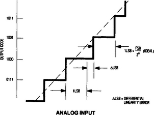
In a DAC, DNL indicates the difference between actual analog voltage change and the ideal (1 LSB) voltage change at any code change. For example, a DAC with a 1.5 LSB step at a code change is said to show a DNL of ½ LSB (see Figs. 2-4 and 2-5). DNL can be expressed in LSB or percentage of full-scale.
In simplified design, DNL specifications are as important as linearity specifications because the apparent quality of a data-converter curve can be markedly affected by DNL, even though linearity is good. For example, Fig. 2-4 shows a curve with ±½ LSB linearity and ± 1 LSB DNL. Figure 2-5 shows a curve with +1¼ LSB linearity and ±½ LSB DNL. In many applications, the curve of Fig. 2-5 would be preferred over that of Fig. 2-4 because the Fig. 2-5 curve is smoother. (In simple terms, DNL describes the smoothness of the curve and is thus of great importance to the user.)
Figure 2-10 shows an exaggerated example of DNL in which the DNL is ±2 LSB and the linearity specification is ± 1 LSB. This results in a transfer curve with a grossly degraded resolution. For example, the normal 8-step curve is reduced to three steps, and a 16-step curve (4-bit converter) with only 2 LSB DNL is reduced to six steps (a nonexistent 2.6-bit device!).
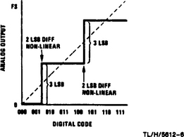
FIGURE 2-10 Exaggerated example of DNL (National Semiconductor, Linear Applications Handbook, 1994, p. 335)
Unfortunately, DNL is not always listed on data sheets by all manufacturers. One reason for this is that DNL is difficult to measure on a production-line basis. Listed or not, DNL can be as much as twice nonlinearity, but never more.
2.5 Monotonicity
Figure 2-11 shows a nonmonotonic DAC transfer curve. For the curve to be nonmonotonic, the linearity error must exceed ±½ LSB by no matter how little. The greater the linearity error, the more significant the negative step might be. On the other hand, a monotonic curve has no change in sign of the slope. All incremental elements of a monotonically increasing curve have positive or zero (but never negative) slope. The converse is true for decreasing curves.
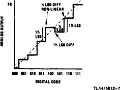
FIGURE 2-11 Nonmonotonic DAC transfer curve (National Semiconductor, Linear Applications Handbook, 1994, p. 336)
A converter showing more than ±½ LSB nonlinearity can still be monotonic up to a certain point, but not beyond that point. For example, a 12-bit DAC with ±½-bit linearity to 10 bits (not a true ±½ LSB) will be monotonic at 10 bits, but might or might not be monotonic at 12 bits (unless tested and guaranteed to be 12-bit monotonic). Finally, a nonmonotonic converter might be acceptable for some applications. However, nonmonotonic converters are disastrous in closed-loop servo systems, including DAC-controlled ADCs.
2.6 Settling Time and Slew Rate
As discussed in Section 1.2.7, settling time is a critical factor in converter performance and is often listed along with slew rate. Settling time is the elapsed time after a code transition for DAC output to reach final value within specified limits, usually ±½ LSB. Slew rate is an inherent limitation of the output amplifier in a DAC, and functions to limit the output voltage rate-of-change after code transitions.
Settling time is often summed with slew rate to obtain total elapsed time for the output to settle to final value. This is shown in Fig. 2-12, which delineates the part of total elapsed time considered to be slew rate and the part that is settling time. As shown, the total time is greater for a major code change than a minor code change because of amplifier slew limitations. However, settling time also can be different, depending on amplifier overload-recovery characteristics.

2.7 Conversion Rate
Both settling time and slew rate (as well as delay in counting circuits, ladder switches, and comparators) affect conversion rate (the speed at which an ADC or DAC can make repetitive data conversions). On some data sheets, conversion time is specified as a number of conversions per second. Other data sheets list conversion rate as the number of microseconds required to complete one conversion (including the effects of settling time). Some data sheets specify conversion rate for something less than full resolution, thus showing a misleading (high) rate.
2.8 Temperature Coefficient and Long-Term Drift
Temperature coefficient (TC) of the various components of a DAC or ADC can produce (or increase) any of several errors when the operating temperature varies. Zero-scale offset error can change because of the amplifier and comparator input-offset TC. Scale error can occur because of shifts in the reference, changes in ladder resistance, change in beta in current switches, or drift in amplifier gain-set resistors. Linearity and monotonicity of the DAC can be affected by different temperature drifts of the ladder resistors and switches. Many other characteristics can be affected by TC. In fact, with the possible exception of resolution and quantizing error, all data-converter characteristics can be affected by temperature changes.
Long-term drift, caused mainly by resistor and semiconductor aging, can affect all characteristics that temperature change can affect. The characteristics most commonly affected by long-term drift are linearity, monotonicity, scale, and offset. Scale changes because reference-voltage changes are usually the most important long-term change or drift problem.
2.9 Overshoot and Glitches
Both overshoot and glitches are essentially DAC problems. However, because most ADCs contain a DAC, ADCs also can be affected. Overshoot and glitches occur whenever a code transition occurs in a DAC. There are two causes. The current output of a DAC contains switching glitches because of possible asynchronous switching of the bit currents (expected to be worst at ½-scale transition when all bits are switched). Although such glitches are of extremely short duration, they could be ½ scale in amplitude. Although the glitches are generally attenuated at the DAC voltage output (because the amplifier is unable to slew at a very high rate), the glitches are coupled around the amplifier through the feedback network. In addition to the glitches, the output amplifier introduces some overshoot and some noncritical damped ringing. These problems can be minimized, but not entirely eliminated (except at the expense of slew rate and settling time, which are much more important).
2.10 Power Supply Rejection
Supply rejection relates to the ability of a DAC or ADC to maintain scale, offset, TC, slew rate, and linearity when the supply voltage is varied. The reference voltage must be constant (unless considering a multiplying DAC). Most affected are current sources (affecting linearity and scale) and amplifiers or comparators (affecting offset and slew rate). Supply rejection is usually specified as a percentage of full-scale change at or near full scale (at 25 °C).
2.11 Input Impedance and Output Drive
Input impedance of an ADC describes the load placed on the analog source. Output drive describes the digital load-driving capability of an ADC or the analog load-driving capacity of a DAC. Output drive is usually given as a current level or a voltage output into a given load.
2.12 Clock Rate
For an ADC, clock rate is the minimum or maximum pulse rate at which the counters can be driven. There is a fixed relation between minimum conversion rate and clock rate that depends on converter accuracy and type. All factors that affect the conversion rate of an ADC limit the clock rate.
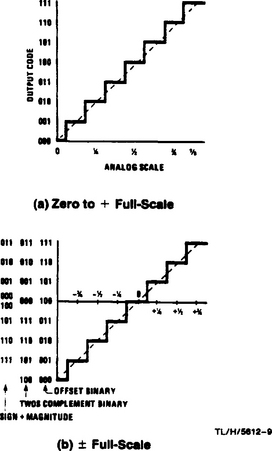
2.13 Data-Converter Codes
Data converters use most of the codes found in other digital equipment. Several types of DAC input, or ADC output, codes are in common (Fig. 2-13). Each code has advantages, depending on the system to be interfaced with the converter. The following is a summary of the most common data-converter codes.
2.13.1 Natural Binary
Natural (or simple) binary is the usual 2n code with 2, 4, 8, 16, … 2n progression. An input or output high, or 1, is considered a signal, whereas 0 is considered an absence of signal. This is a positive-true binary signal. Zero scale is all zeros, and full scale is all ones.
2.13.2 Complementary Binary
Complementary (or inverted) binary is the negative-true binary system. It is identical to natural binary except that all binary bits are inverted. Thus zero scale is all ones, and full scale is all zeros.
2.13.3 Binary Coded Decimal
Binary coded decimal (BCD) is the representation of decimal numbers in binary form. It is useful in ADC systems intended to drive decimal displays. The advantage of BCD over decimal is that only four lines are needed to represent 10 digits. The disadvantage of BCD is that a full 4 bits can represent 16 digits, whereas only 10 digits are represented in BCD. The full-scale resolution of a BCD-coded system is less than that of a binary-coded system. For example, a 12-bit BCD system has a resolution of only one part in 1,000 compared with one part in 4,098 for a binary system. This represents a loss of resolution of more than 4:1.
2.13.4 Offset Binary
Offset binary is a natural binary code, except that it is offset (usually ½ scale) to represent negative and positive values. Maximum negative scale is represented as all zeros and with maximum positive scale as all ones. Zero scale (actually center scale) is then represented as a leading 1 and all remaining 0s.
2.13.5 Two’s Complement Binary
Two’s complement binary is widely used to represent negative values. With two’s complement, zero and positive values are represented as in natural binary, and all negative values are represented in a two’s complement form (see Fig. 2-13). That is, the two’s complement of a number represents a negative value so that interface to a computer or microprocessor is simplified.
The two’s complement is formed by complementing each bit and then adding a 1. Any overflow is neglected. For example, the decimal number − 8 is represented in two’s complement as follows: start with a binary code of decimal 8 (off scale for ± representation in 4 bits, so not a valid code in the ± scale of 4 bits), which is 1000. Complement this number to 0111 and add 0001 to get 1000.
The offset-binary representation of the ± scale differs from the two’s complement representation only in that the MSB is complemented. The conversion from offset binary to two’s complement requires that only the MSB be inverted.
2.13.6 Sign Plus Magnitude
As shown in Fig. 2-13, sign plus magnitude contains polarity information in the MSB. (When the MSB is 1, the number is negative.) All other bits represent magnitude only. One code is used up providing a double code for zero (000 or 100). Sign plus magnitude code is used in certain instrument applications (such as digital volt-meters [DVMs]) and in audio circuits. The advantage in both applications is that only one bit has to be changed for small-scale changes when the value is near zero and plus and minus scales are symmetric.