Practical Design Considerations
Now that we know how data converters work and we have settled on some basic terms, let us discuss practical design considerations. The remaining chapters in this book describe how a specific IC data converter can be used. The information in this chapter applies to all data converters, both ADC and DAC, and is included primarily so that the reader can select a converter to suit a specific system need. This should keep overspecification (with the usual high cost) to a minimum.
When reading this chapter, and all subsequent chapters, keep in mind that specific parameters, test conditions, test circuits, and even definitions might vary from manufacturer to manufacturer. For practical production reasons, parameters might not be tested in the same way for all converter types, even those supplied by the same manufacturer. However, using the information in this and remaining chapters, you should be able to sort out and understand specifications (from any manufacturer) that apply to your application.
3.1 Digital Control Signals
Data converters are digital devices and thus require digital control signals. Each ADC must accept or provide digital control signals telling it or the external system what to do and when to do it. Control signals should be compatible with one or more types of logic (TTL, CMOS, ECL) in common use. Control-signal timing must be such that the converter (or system) accepts the signals. The following is a summary of control signals found in most practical applications.
3.1.1 Start Conversion
Start conversion (SC) is a digital signal to an ADC that initiates a single conversion cycle. An SC signal typically must be present at the fall (or rise) of the clock waveform to initiate the cycle. A DAC needs no SC signal. However, an SC signal can be provided to gate digital inputs to a DAC.
3.1.2 End of Conversion
End of conversion (EOC) is a digital signal from an ADC that informs the external system that the digital output data bits are valid. Typically, an EOC output can be connected to an SC input to cause the ADC to operate in a continuous-conversion mode. In noncontinuous systems, the SC signal is a command from the system to the ADC. A DAC does not supply an EOC signal.
3.2 Voltage References
As discussed in Chapter 1, data converters require a voltage reference. Most present-day IC converters have internal references. Figure 3-1 shows some typical examples. The suitability of a reference for a particular application depends mostly on accuracy and drift. As shown in Fig. 3-1, typical accuracy ranges from 0.2% to 1.63% for different ADCs.

FIGURE 3-1 Typical ADC internal reference accuracy and drift (Maxim New Releases Data Book, 1992, p. 7-10)
From a simplified-design standpoint, reference accuracy and temperature drift relate directly to full-scale errors. If absolute accuracy is required, a precision reference must be used. If the requirements are too demanding for the internal reference, many converter ICs also accept external references (and there are converter ICs without internal references). Keep in mind that references with higher untrimmed accuracy cost more. So, if you are concerned primarily with stability and repeatability over a given temperature range, look for a reference with a low temperature coefficient (TC), but with less accuracy and a lower cost. Also remember that the reference on some IC converters can be trimmed to a given accuracy. However, this involves external components (with added cost and space consumption).
3.2.1 Ratiometric Data Conversion
One solution to the reference-accuracy problem is to use a ratiometric system in which the same reference drives both the converter and the external system or device. With ratiometric, the actual reference-voltage value (along with the error and drift) does not affect the result. If the reference voltage increases with temperature (or vice versa) both the converter and system change by the same ratio. As a result, the reference voltage need not show perfect stability over time and temperature. Either the data converter or an external source can provide the reference. In many applications, the power-supply voltage can be used as the reference (if the system supply is free from noise).
Of course there are applications in which absolute accuracy is required. For example, a direct voltage measurement using a digital meter (based on use of an ADC) is absolute and requires absolute reference accuracy. A ratiometric system should not be used in such cases.
A ratiometric system can be used when the information to be converted is the output signal from a bridge-type transducer fed into an ADC. The bridge output (for example, from a load cell or pressure transducer) is a function of the quantity (weight, pressure) and the bridge-excitation voltage. If the converter reference (or an external reference) is used for bridge excitation, variations in reference voltage will be applied equally (and in the same ratio).
3.3 Multichannel Conversion
When many channels of data must be converted, special problems arise in selecting a data-converter IC or system. The following is a summary of these problems and possible solutions.
3.3.1 Data Converters with Built-in Multiplexers
Unless the information to be converted is in a system with unlimited space (and high cost can be tolerated), some form of multiplexer must be used. For example, when several analog inputs are measured, a signal multiplexer is usually used at the ADC input. The multiplexer can be external, or an ADC with internal multiplexer (such as shown in Fig. 3-2) can be used. Such ADC ICs also offer some performance advantages over an external multiplexer ADC combination, besides providing the advantage of component savings. Multiplexer-error contributions and settling-time delays are eliminated from system specifications because they are included in the ADC error and timing limits. For example, the MAX180 shown in Fig. 3-2 has a 7.5-μs conversion time. This includes the time used by the multiplexer, the track-and-hold (T/H), and the ADC function.

FIGURE 3-2 12-bit ADC with on-chip multiplexer, track-and-hold, and internal reference (Maxim New Releases Data Book, 1992, p. 7-11)
Another advantage of the single-chip ADC with built-in multiplexer is that the interface is simplified. Only one device has to be addressed. In the IC of Fig. 3-2, the same operation can be used to select a channel and start a conversion. This cuts down on decoding logic and saves power.
3.3.2 Data Converters with External Multiplexers
Although multiple-input ADCs provide both convenience and performance advantages, such ICs have limitations that a separate ADC and multiplexer can sometimes overcome. An example is when the relative timing of multiplexed signals is critical. A typical ADC with multiplexer (one-chip or not) measures each channel in sequence—channel 1 is read long before channel 8, and so on. In some systems, this might add error if the signals of interest occur at the same time (the relative phase might contain information that the channel scanning distorts).
One solution to the timing problem is to scan and convert at a fast rate so that the time delay between channels is reduced to insignificant levels. This requires higher clock speed (along with the usual higher cost and possibly higher power consumption). Another solution is to scan or sample all input channels at the same time, then multiplex through T/H circuits before conversion. This eliminates scan-timing errors. (CMOS converters work well with such an approach.)
Any data-converter system with multiple inputs works best when all input levels have a similar dynamic range. If filtering or widely different channel gain is needed in a system, an IC with internal multiplexing usually requires that each channel has its own signal-conditioning circuit (a repetitive and expensive solution). This problem can be overcome with a single filter and programmable amplifier between an external multiplexer output and an ADC input.
The IC of Fig. 3-2 uses this technique, but does not require an external multiplexer. The output of the six-channel multiplexer (mux) and the input of the ADC are on separate pins, so a lowpass filter can be connected between the two. (A lowpass filter, such as the MAX270, provides selectable fourth-order corner frequencies between 1 kHz and 20 kHz for different channels.)
The final advantage of a separate multiplexer is that greater fault protection can be provided. Most present-day ADC ICs do not have high-voltage fault protection because structures are too large. Even when input-limiting resistors and external clamp diodes are used on each channel, there can be problems. (Crosstalk, caused when inactive channels are driven beyond the supply voltage, is a typical problem.) If such small, but significant, errors cannot be tolerated, an external multiplexer with high fault protection is the best solution. For example, the MAX358 or MAX378 fault-protected analog multiplexers can withstand up to 70-V overloads without spilling overdrive signals through to selected channels (crosstalk).
3.4 Track and Hold
Many ADCs include T/H functions as part of the internal circuit (such as the IC of Fig. 3-2). The T/H prevents the input from moving during the successive-approximation conversion process. As a (theoretic) guideline, a T/H function is required if the input signal changes during the time required for conversion to ½ LSB.
It is often assumed that T/H is not required for high-speed ADCs because conversion is complete before any significant changes occur. Although this is generally true, there are limitations. For example, assume a 12-bit ADC with 3.3-μs conversion time and a 5-V full-scale range. Such an ADC resolves changes in inputs of less than a millivolt. Signals well below 1 kHz change by this amount in less than 3.3-μs conversion time. As a simplified-design guideline, a T/H function is required for input frequencies above about 10 Hz, if 12-bit performance is to be maintained in an ADC with 3- to 3.5-μs conversion time.
Another advantage of an ADC with T/H is that there are no transient loads on the signal source. ADCs without T/H (especially high-speed ADCs) affect the signal lines. If the signal source does not settle in time for the bit decision, the ADC comparator bases its decision on false information, resulting in converter noise and nonlinearity at best, and possible inaccuracy at worst. This is true even for low-frequency signals that do not violate the ½ LSB rule and causes many successive-approximation ADCs (and even some flash ADCs) to place high demands on the signal source, particularly with 12 bits and more.
A sampling ADC converter (with mux and T/H as shown in Fig. 3-2) demands very little from the signal source in terms of dynamic capability, even though the ADC is of the successive-approximation type. Current is drawn from the input source only once when the input is sampled, not on each bit test. This accommodates a much wider variety of signal sources without buffering.
3.5 Interfacing
The ideal data-converter interface is fast, requires a minimum of hardware (preferably the existing buses and control lines) and existing software (available microprocessor control signals). Unfortunately, the specific converter interface architecture that accomplishes this varies widely with application. Common microprocessors use 8- and 16-bit buses. Microcontrollers use 4- and 8-bit buses. Both can use serial interfaces.
Figure 3-3 shows the timing diagram of the control interface between a typical ADC (the MAX163/4/7) and a microprocessor. This particular ADC connects to either 8- or 16-bit buses, and has selectable interface modes using only one or two control lines. In one configuration, the microprocessor can start a conversion, perform other tasks, and then come back to read data. In the other mode, the microprocessor starts with a read (![]() ), and waits until the ADC supplies the answer. The microprocessor uses a
), and waits until the ADC supplies the answer. The microprocessor uses a ![]() output on the ADC to stretch the read cycle. This makes the ADC appear like a slow-memory device to the system.
output on the ADC to stretch the read cycle. This makes the ADC appear like a slow-memory device to the system.
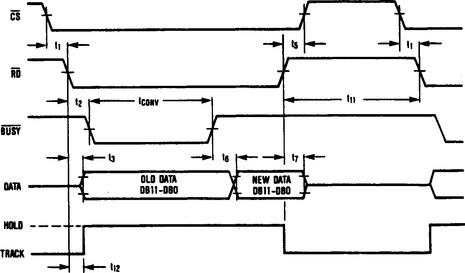
FIGURE 3-3 Timing diagram of control interface between ADC and microprocessor (Maxim New Releases Data Book, 1992, p. 7-13)
3.5.1 Serial Interface
Serial interfaces can provide major advantages, especially in data-acquisition designs, in which size and board space are often at a premium. Consider the space requirements of two equivalent 12-bit ADCs. A serial device (such as the MAX170) fits into an 8-pin package, whereas a parallel ADC (the MAX162/172) uses 24 pins. In addition, because of the narrow data path (typically no more than three lines) the serial device does not affect conversion time. Serial interfaces should also be considered when designing electrically isolated systems (see Section 3.5.2).
3.5.2 Electrical Isolation with Opto-Coupling
Some operating environments do not allow electrical connection between the signal source and the measuring system. This is a frequent safety requirement in industrial applications in which it is possible for the input signals to be “hot” in reference to the AC power line, either unintentionally or by design. The most common method for electrical isolation in data-conversion systems is opto-coupling. Figure 3-4 shows an ADC with full electrical isolation in which three opto-coupled lines are used (serial data, clock, and conversion start).

With opto-couplers to isolate data lines, the ADC transmits information, but without direct electrical connection to the microprocessor (or other system device). Both the ADC and analog input signal are isolated from the processor and system. A serial ADC works best because only the three interface lines require opto-couplers.
Isolation provided by the ADC of Fig. 3-4 also has the advantage of noise reduction by eliminating ground loops and by providing superior common-mode rejection to most differential-input devices. This is especially useful in large systems in which signals from many remote locations are returned to one point.
Each signal return line is likely to be at a slightly different potential, so ground-loop currents are almost certain.
3.6 Conversion Speed
Some ADC manufacturers specify operating speed in terms of conversion time (the time required for one conversion). Other manufacturers use conversions (or samples) per second. Although these two terms are closely related, the true conversion rate does not always translate exactly to the inverse of conversion time. This is because ADCs often require time between conversions.
Figure 3-5 shows the timing diagram of a typical ADC (the MAX167) that performs a conversion in 7.81 μs (12.5 clock cycles), if the start of the conversion is synchronous with a 1.6-MHz clock. Data-access timing limits prevent the next conversion from starting immediately. However, keeping the times as short as possible, and guaranteeing data-bus timing specifications over a given temperature range, minimizes dead time between conversions. This allows the ADC continuously to perform 100,000 samples per second, including the operating time of the internal T/H circuits.

The ADC of Fig. 3-5 can “pipe line” the output data bits to increase interface speed. This means that as each new conversion is started by a signal on ![]() (read), the results of the last conversion (the digital bits representing the analog input) immediately appear on the data bus. The data bits are always one conversion old but can be accessed without waiting. Separate read and write commands are not needed.
(read), the results of the last conversion (the digital bits representing the analog input) immediately appear on the data bus. The data bits are always one conversion old but can be accessed without waiting. Separate read and write commands are not needed.
3.7 AC Signal Processing
When an ADC measures an AC signal, deviations from the ideal-converter transfer function generate noise and distortion in the digital-output data. The severity of these distortions might not correlate with classic ADC specifications, such as offset, linearity, and full-scale error. In general, large offset and full-scale errors do little harm to AC performance. The effect on linearity usually depends more on the shape of the error rather than the amplitude. From a simplified-design standpoint, converter noise expressed as a portion of an LSB does not indicate the effect on dynamic signals. What is important for DC-signal measurements is not necessarily important for AC signals.
3.8 Noise Problems
Noise pickup can be a problem when converting any analog signal to digital, but it is particularly troublesome when the analog-signal amplitudes are small (about 100 mV or less). As a simplified-design guideline, make the ADC conversion as close to the source as practical. (This is easily done with small, serial-output ADCs such as the MAX170.) Another simplified-design technique is to amplify the analog inputs (again near the source) to the highest practical level. In any ADC or DAC system, try to minimize noise pickup by routing any low-level signals away from clock lines, relays, and any other noisy switching circuits.
3.8.1 Nodes Particularly Susceptible to Noise
The following circuit nodes or points often have noise problems:
1. ADC input pins not driven from a buffered source
2. The investing inputs of op amps
These nodes or points should be made as physically small as practical to reduce coupling from noise sources. Analog circuits should be separated from digital circuits on the board whenever practical. In the case of very low-level analog signals, separately shielded subcircuits should be used if possible.
3.8.2 Using Buffers
Some data converter systems (especially ADCs) might require buffers, particularly in circuits in which there are missing codes or noise, even when the source and physical layout are clean. The problem might be at the ADC input. Many successive-approximation ADCs (those without T/H) are difficult to drive and should have input buffers.
Use the following simplified-design test to determine if buffers are needed (or would greatly improve performance). Slow the system clock down to about half speed. This allows the input source more time to settle after being loaded by the ADC input circuits. If a slower clock cures the noise problem (restores any missing codes), the input signal probably needs a buffer. Try the circuit with a buffer at the normal clock speed as a final check.
3.8.3 Noise and the ADC Reference
In many data-acquisition applications, the fact that the ADC reference input also acts as an analog input is often overlooked. This is important because some ADC architectures are less effective than others in rejecting reference noise. For example, if the reference voltage settles poorly in response to current demands in the ADC IC, noise can result. So if you have noise that cannot be cured by any of the other methods described in this section, try an ADC with different architecture in the same circuit.
3.9 Practical Layout
The following tips apply to all of the simplified design examples in the remaining chapters of this book.
3.9.1 Single-Point Grounding
Try to connect all signal, ADC/DAC, and power grounds to a single point. This minimizes ground loops that could generate unwanted currents produced by stray magnetic fields. Single-point grounding also prevents the voltage drop in current-carrying lines from affecting the ground reference of more sensitive circuits.
3.9.2 Separate Power Supplies
If practical, use separate power supplies for the analog and digital circuits. Ideally, analog and digital circuits should be completely isolated from one another, especially for precision measurement applications. If separate supplies are not practical, connect the analog and digital circuits to the single system supply through separate RC filters.