
Simplified Design with a Typical ADC
This chapter is devoted to simplified-design approaches for a typical ADC IC. All of the general design information in Chapters 1 through 3 applies to the examples in this chapter. However, each data-converter IC has special design requirements, all of which are discussed in detail. The circuits in this chapter can be used immediately the way they are or, by altering component values, as a basis for simplified design of similar data-converter applications. The chapter concludes with a fully isolated 12-bit ADC using serial-to-parallel conversion.
4.1 General Description of ADC
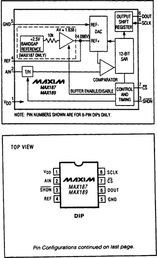
Figure 4-1 shows the functional block diagram and pin configuration for the ADC (a MAX187/189). This serial-bit IC operates from a single +5-V supply and accepts a 0-V to 5-V analog input. The ICs feature an 8.5-μs SAR, a 1.5-μs T/H, an on-chip clock, and a high-speed serial interface. An external clock accesses data from the interface, which communicates without external hardware to most digital processors and microcontrollers. The interface is compatible with SPI™, QSPI™, and Microwire™. The ICs digitize signals at a 75-ksps (75,000 samples per second), with a normal power consumption of 7.5 mW, and a shutdown power of 10 μW. The MAX187 has an on-chip buffered reference. The MAX189 requires an external reference.
4.2 Data-Converter Operation
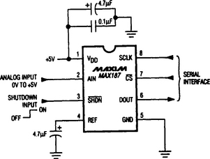
Figures 4-2 and 4-3 show the ADCs in their simplest configurations. Figure 4-4 shows the pin descriptions. As shown in Figure 4-1, the ICs use input T/H and a 12-bit SAR to convert an analog input signal to a digital 12-bit output, as described in Chapter 1. No external-hold capacitor is needed for the T/H. Conversion of input signals in the 0-V to Vref range are converted in 10 μs, including the T/H acquisition time. The internal reference of the MAX187 is trimmed to 4.096 V. Both ICs can accept external references from +2.5 V to Vdd.

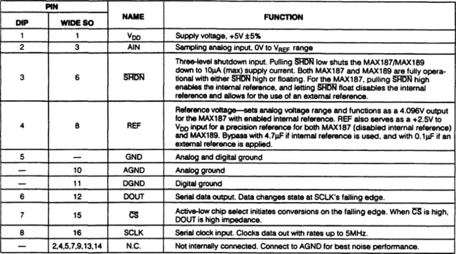
The serial interface requires only three digital lines, SCLK, ![]() , and DOUT (Fig. 4-4) to provide easy interface to microprocessors. There are two operating modes: normal and shutdown. Pulling the
, and DOUT (Fig. 4-4) to provide easy interface to microprocessors. There are two operating modes: normal and shutdown. Pulling the ![]() pin low shuts the IC down and reduces supply current to less than 10 μA. Pulling
pin low shuts the IC down and reduces supply current to less than 10 μA. Pulling ![]() high (or leaving the pin floating) puts the IC in the operating mode. A conversion is initiated by making
high (or leaving the pin floating) puts the IC in the operating mode. A conversion is initiated by making ![]() low. The conversion result is available at DOUT in unipolar serial format. A high bit that signals end of conversion (EOC) followed by the data bits (MSB first) makes up the serial data stream. The MAX187 internal reference is selected when
low. The conversion result is available at DOUT in unipolar serial format. A high bit that signals end of conversion (EOC) followed by the data bits (MSB first) makes up the serial data stream. The MAX187 internal reference is selected when ![]() is formed high.
is formed high. ![]() is left floating to select external reference.
is left floating to select external reference.
4.2.1 Analog Input
Figure 4-5 shows the equivalent analog-input circuits. The full-scale input voltage depends on the voltage at REF, as described in Fig. 4-4. Note that a bypass is recommended at the REF pin for both internal and external reference configurations.
4.2.2 Track and Hold
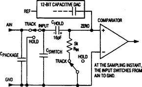
In the track mode, the analog signal is acquired and stored in the internal hold capacitor (CHOLD) (Fig. 4-5). In hold mode, the T/H switches open and maintains a constant input to the SAR circuits. During acquisition, the analog input (AIN) charges CHOLD. Bringing ![]() low ends the acquisition interval. At this instant, the T/H switches the input side of CHOLD to ground (GND). The retained charge on CHOLD represents a sample of the input, unbalancing the ZERO point at the comparator input.
low ends the acquisition interval. At this instant, the T/H switches the input side of CHOLD to ground (GND). The retained charge on CHOLD represents a sample of the input, unbalancing the ZERO point at the comparator input.
In the hold mode, the capacitive DAC adjusts during the remainder of the conversion cycle to restore the ZERO point to 0V, within the limits of a 12-bit resolution. This action is equivalent to transferring a charge from CHOLD to the binary-weighted capacitive DAC, which forms a digital representation of the analog input signal. At the end of conversion, the input side of CHOLD switches back to AIN, and CHOLD charges to the input signal again.
In any ADC with T/H at the input, the time required for the T/H to acquire an input signal is a function of how quickly the input capacitance is charged. If the input-signal source impedance is high, the acquisition time is longer, and more time must be allowed between conversions. The acquisition time for these ADCs is calculated as follows: acquisition time = 9 (Rs + Rin) 16 pF, where Rin is 5k, Rs is the source impedance of the input signal, and the time is never less than 1.5 μs. For simplified design, source impedances less than 5k do not significantly affect the AC performance of these ADCs.
4.2.3 Input Bandwidth
The input-tracking circuit has a 4.5-MHz small-signal bandwidth, and an 8 V/μs slew rate. It is possible to convert (or digitize) high-speed events and measure periodic signals when the bandwidths exceed the sampling rate. This requires undersampling, however, and is generally not recommended unless an ADC with a higher sampling rate is not practical. One problem with undersampling is aliasing of unwanted high-frequency signals into the frequency band of interest. This can be overcome with an anti-alias filter, but that requires additional components (see the MAX274/MAX275 continuous-time filter data sheet for filter information). For simplified design, use an ADC with a higher sampling rate (if possible), such as described in Chapter 5.
4.2.4 Input Protection
The ADCs in this chapter are provided with internal protection diodes that clamp the analog input to swing from GND − 0.3 V to Vdd + 0.3 V without damage. However, for accurate conversions near full scale, the input must not exceed Vdd by more than 50 mV or be lower than GND by 50 mV. If the analog input exceeds the supplies by more than 50 mV in either direction, limit the input current to 2 mA. Any larger currents can degrade conversion accuracy on these ADCs. There is usually a similar limit for most ADCs.
4.2.5 Analog Input-Drive Amplifiers
The input lines to AIN and GND should be kept as short as possible to minimize noise pickup (a classic guideline for all ADCs, and most ICs). Shield any leads that must be long. Because these ADCs have a T/H input, the drive requirements of the op amp driving AIN are less stringent that those in which no T/H is provided. (That is one of the major benefits of T/H inputs in an ADC.) A typical input capacitance for these ADCs is 16 pF.
The input amplifier must have sufficient bandwidth to handle the frequency of the input signal. The manufacturer recommends a MAX400 and 0P07 for lower frequencies and a MAX427 and OP27 for higher frequencies. Keep in mind that the allowed input frequency range is limited by the 75-ksps sample rate. Therefore, the maximum sinusoidal input frequency allowed is one-half or 37.5 kHz. Higher-frequency signals cause aliasing problems.
4.2.6 Internal Reference
The internal reference of the MAX187 is connected to the REF pin and to the internal DAC. This reference can source up to 0.6 mA for use by external components connected to the REF pin. Decouple the REF pin to ground with a 4.7-μF capacitor. The internal reference can be disabled when ![]() is left floating. This allows use of an external reference.
is left floating. This allows use of an external reference.
4.2.7 External Reference
If an external reference is used (always for MAX189 and when the MAX187 internal reference is disabled), stay within the voltage range from +2.5 V to Vdd. The external reference must be capable of delivering up to 350 μA with an output impedance of 10 ohms or less. Decouple the REF pin to ground with a minimum of 0.1 μF. If the reference has a high output impedance (or is noisy), use 4.7 μF for the bypass.
4.3 Serial Interface Considerations
Figure 4-6 shows the complete conversion sequence of the serial interface lines, including the shutdown sequence. Figures 4-7 and 4-8 show details of the interface timing sequence. The following paragraphs summarize the serial-interface functions.
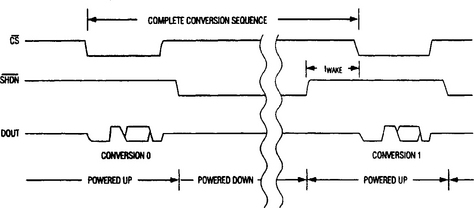
FIGURE 4-6 Complete conversion sequence of serial-interface lines including shutdown (Maxim New Releases Data Book, 1995, p. 7-52)


FIGURE 4-8 MAX187/189 detailed serial-interface timing (Maxim New Releases Data Book, 1995, p. 7-54)
4.3.1 Initialization and Conversion Start
When power is first applied, it takes the fully discharged 4.7-μF reference-bypass capacitor about 20 ms to provide adequate charge (for specified accuracy). With ![]() not pulled low, the ADCs are now ready to convert.
not pulled low, the ADCs are now ready to convert.
To start a conversion, pull ![]() low. At the falling edge of
low. At the falling edge of ![]() , the T/H enters the hold mode, and a conversion is initiated. After an internally timed 8.5-μs conversion period, the end of conversion is indicated when DOUT goes high. Data can then be shifted out serially with the external clock.
, the T/H enters the hold mode, and a conversion is initiated. After an internally timed 8.5-μs conversion period, the end of conversion is indicated when DOUT goes high. Data can then be shifted out serially with the external clock.
4.3.2 Reducing Supply Current
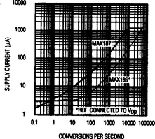
You can reduce power consumption considerably by shutting down the ICs between conversions. This is shown in Fig. 4-9. Because the MAX189 uses an external reference voltage, it “wakes up” faster than the MAX187 and thus provides lower average supply currents. The wakeup time (tWAKE) is the time from deassertion of ![]() to the time when a conversion can be initiated. For the MAX187, this time is 2 μs. For the MAX189, this time depends on the time in shutdown (Fig. 4-10). This is because the external 4.7-μs reference bypass capacitor loses its charge slowly during shutdown.
to the time when a conversion can be initiated. For the MAX187, this time is 2 μs. For the MAX189, this time depends on the time in shutdown (Fig. 4-10). This is because the external 4.7-μs reference bypass capacitor loses its charge slowly during shutdown.

4.3.3 External Clock
The actual conversion does not need the external clock. This frees the microprocessor from the burden of running the SAR conversion clock and allows the conversion result to be read back at the convenience of the microprocessor at any clock rate from 0 MHz to 5 MHz. The clock duty cycle is unrestricted if each clock phase is at least 100 ns. Do not run the clock while a conversion is in progress.
4.3.4 Timing and Control
As shown in Figs. 4-7 and 4-8, conversion-start and data-read operations are controlled by the ![]() and SCLK digital inputs. A
and SCLK digital inputs. A ![]() falling edge initiated a conversion sequence: the T/H falling edge holds input voltage, the ADC begins to convert, and DOUT changes from high impedance to logic low. SCLK must be kept inactive during the conversion. An internal register stores the data when the conversion is in progress.
falling edge initiated a conversion sequence: the T/H falling edge holds input voltage, the ADC begins to convert, and DOUT changes from high impedance to logic low. SCLK must be kept inactive during the conversion. An internal register stores the data when the conversion is in progress.
End of conversion (EOC) is indicated by DOUT going high. The DOUT rising edge can be used as a framing signal. SCLK shifts the data out of the register any time after the conversion is complete. The DOUT transitions occur on the SCLK falling edge. The next falling clock-edge produces the MSB of the conversion at DOUT, followed by the remaining bits.
Because there are 12 data bits and one leading high bit, at least 13 falling clock edges are needed to shift out a full set of bits. Extra clock pulses after the conversion result has been clocked out and before a rising edge of ![]() produce trailing 0s at DOUT and have no effect on converter operation.
produce trailing 0s at DOUT and have no effect on converter operation.
To get minimum cycle time, use the DOUT rising edge as the EOC signal. Clock out the data with 13 clock cycles at full speed, and raise ![]() after the LSB of the conversion has been read. After the specified minimum acquisition time (tACQ),
after the LSB of the conversion has been read. After the specified minimum acquisition time (tACQ), ![]() can be pulled low again to initiate the next conversion.
can be pulled low again to initiate the next conversion.
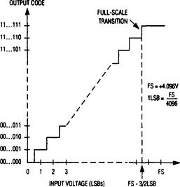
4.3.5 Output Coding and Transfer Function
As shown in Fig. 4-11, the data output from these ADCs is binary (unipolar), and code transitions occur halfway between successive integer LSB values. If Vref is +4.096 V (the trimmed value for the MAX187), then 1 LSB = 1.00 mV or 4.096V/4096.
4.4 Dynamic Performance Characteristics and Testing
As discussed in Chapter 2, ADCs are often tested for such characteristics as zero error, full-scale error, integral nonlinearity (INL), and differential nonlinearity (DNL). These tests are generally sufficient when the ADC is used to convert DC and slowly varying signals. However, when the ADC is used with dynamic input signals (wideband signal processing), other tests and parameters are of much greater importance. The following paragraphs summarize the most important dynamic tests from a simplified-design standpoint.
4.4.1 Fast Fourier Transforms
Figure 4-12 shows a fast fourier transform (FFT) plot using a spectrum analyzer for the MAX187/189. Such tests guarantee the dynamic frequency response, distortion, and noise at the rated throughput (combination of sampling frequency and total or test frequency) of the ADC. The test involves applying a low-frequency sine wave to the ADC input and recording the digital conversion results for a specified time. The data bits are then analyzed using an FFT algorithm that determines the spectral content. Conversion errors are seen as spectral elements outside the fundamental input frequency.

4.4.2 SINAD and Effective Number of Bits
SINAD (signal-to-noise plus distortion) is the ratio of the RMS amplitude of the fundamental input frequency to the RMS amplitude of all other ADC output signals. The input bandwidth is limited to frequencies above DC and below one-half of the ADC sample (conversion) rate.
The theoretic minimum ADC noise is caused by quantization error and is a direct result of the resolution of the ADC: SINAD = (6.02N + 1.76) dB, where N is the number of bits of resolution. An ideal 12-bit ADC can therefore do no better than 74 dB. However, as shown in Fig. 4-12, there is an output signal (at about 12 kHz) greater than 80 dB above signals of other frequencies.
The effective number of bits (or effective resolution) that can be provided by an ADC is determined by transposing the SINAD equation and substituting the measured SINAD: N = (SINAD – 1.76)/(6.02). Figure 4-13 shows the effective number of bits as a function of input frequency for the MAX187/189.

4.4.3 Total Harmonic Distortion
If a pure sine wave is sampled by an ADC at greater than the Nyquist frequency, the nonlinearities in the transfer function of the ADC produce harmonics of the input frequency present in the sampled output data. For an ADC, total harmonic distortion (THD) is the ratio of the RMS sum of all harmonics (in the frequency band above DC and below one-half the sample rate, but not including the DC component) to the RMS amplitude of the fundamental frequency. This is expressed as:
where V1 is the fundamental RMS amplitude, and V2 through VN are the amplitudes of the second through Nth harmonics. (The THD specification for the MAX187/189 is − 80 dB maximum, with a 10-kHz sine wave, from 0 V to 4.096 Vp–p, sampled at 75 ksps).
4.4.4 Using the Dynamic Characteristics
For simplified design, it is not usually necessary to test all the dynamic characteristics. Simply use the ADC data-sheet characteristics. For example, if you are concerned with accuracy, the relative accuracy (a DC specification) for the top of the line (MAX187A/MAX189B) is ±½ LSB. Figure 4-13 shows that the effective bits (or effective resolution) is within ½ LSB at input frequencies up to and more than 20 kHz. Therefore it is reasonable to assume that both accuracy and resolution are within the ½-bit limit over the same input-frequency range.
One exception to this simplified rule is a situation in which the input frequency is near the test limits or the rated limits of the ADC. Should that occur, you can test the ADC in a basic circuit (Figs. 4-2 and 4-3), as described in Section 1.4.9, at the maximum input frequency. If the ADC performs properly, but you are still unsure, increase the input frequency to well beyond anticipated value (say at 1.5 or 2 times the maximum), and repeat the accuracy tests. If the ADC does not provide the required accuracy at (or slightly above) the maximum frequency, it may be necessary to use another ADC (probably at greater expense). Chapter 5 describes ADCs suitable for high-frequency input signals.
4.5 Applications Data
The remainder of this chapter describes how the MAX187/189 can be used for specific applications.
4.5.1 Standard Interfaces (General Instructions)
Figure 4-14 shows the basic connections for interface between the MAX187/189 and the three common or standard serial-interface configurations. Keep the following in mind when using any of the three interfaces.

FIGURE 4-14 MAX187/189 interface to three common configurations (Maxim New Releases Data Book, 1995, p. 7-56)
Set the microprocessor or CPU (central-processing unit) serial interface in the master mode so that the CPU will generate the serial clock. Choose a clock frequency up to 2.5 MHz.
Use a general-purpose I/O (input-output) line on the CPU to pull ![]() low. Keep SCLK low.
low. Keep SCLK low.
Wait for the maximum conversion time (8.5 μs) specified before activating SCLK. As an alternative, look for a DOUT rising edge to determine the end of conversion.
Activate SCLK for a minimum of 13 clock cycles. The first falling clock edge will produce the MSB of the DOUT conversion. The transition for DOUT data occurs on the SCLK falling edge and is available in MSB-first format. Observe the SCLK to DOUT valid-timing characteristics (Figs. 4-6 through 4-8). Data can be clocked into the microprocessor on the SCLK rising edge.
Pull ![]() high at or after the 13th falling clock-edge. If
high at or after the 13th falling clock-edge. If ![]() remains low, trailing zeros are clocked out after the LSB.
remains low, trailing zeros are clocked out after the LSB.
With ![]() high, wait the minimum specified time (tCS) before launching a new conversion by pulling
high, wait the minimum specified time (tCS) before launching a new conversion by pulling ![]() low. (The minimum tCS is 500 ns for these ADCs.) If a conversion is aborted by pulling
low. (The minimum tCS is 500 ns for these ADCs.) If a conversion is aborted by pulling ![]() high before the conversion ends, wait for the minimum acquisition time (tACQ) before starting a new conversion. (The minimum tACQ is 1.5 μs.)
high before the conversion ends, wait for the minimum acquisition time (tACQ) before starting a new conversion. (The minimum tACQ is 1.5 μs.)
The data bits can be output in 1-byte chunks or continuously (Fig. 4.7). The bytes contain the result of the conversion, padded with one leading 1, and trailing 0s, if SCLK is still active with ![]() kept low.
kept low.
4.5.2 SPI™ and Microwire™ Interface
Figure 4-15 shows the serial interface timing when the MAX187/189 is used with SPI™ or Microwire™. (Note that with SPI™, it is necessary to set the interface CPOL and CPHA lines to 0.)

FIGURE 4-15 Serial interface timing for SPI™ or Microwire™ (Maxim New Releases Data Book, 1995, p. 7-57)
Conversion starts with a ![]() falling edge. DOUT goes low, indicating a conversion in progress. Wait until DOUT goes high (or the maximum specified 8.5 μs conversion time). Two consecutive 1-byte reads are required to obtain the full 12 bits. Output-data (DOUT) transitions occur on the SCLK falling edge and are clocked into the microprocessor on the SCLK rising edge. As shown in Fig. 4-15, the first byte contains a leading 1 as well as 7 bits of conversion. The second byte contains the remaining 5 bits and three trailing zeros.
falling edge. DOUT goes low, indicating a conversion in progress. Wait until DOUT goes high (or the maximum specified 8.5 μs conversion time). Two consecutive 1-byte reads are required to obtain the full 12 bits. Output-data (DOUT) transitions occur on the SCLK falling edge and are clocked into the microprocessor on the SCLK rising edge. As shown in Fig. 4-15, the first byte contains a leading 1 as well as 7 bits of conversion. The second byte contains the remaining 5 bits and three trailing zeros.
4.5.3 QSPI™ Interface
Figure 4-16 shows the serial interface timing when the MAX187/189 is used with QSPI™. (Again, it is necessary to set the interface CPOL and CPHA lines to 0.) Unlike SPI™, which requires two 1-byte reads to acquire the 12 bits of data from the ADC, QSPI™ allows the minimum number of clock cycles necessary to clock the data. The ADCs require 13 clock cycles from the microprocessor to clock out the 12 bits of data with no trailing 0s. The minimum clock frequency to ensure compatibility with QSPI™ is 2.77 MHz.

4.5.4 Fully Isolated Serial-to-Parallel Conversion
Figure 4-17 shows the MAX187 connected to provide full 12-bit ADC operation with serial-to-parallel conversion. This circuit operates from a single 5-V supply and is fully isolated using opto-couplers. The circuit is well suited to industrial applications in which the control electronics must be separated or isolated from hazardous electrical conditions. The circuit also provides noise immunity and prevents excessive current flow where there are different ground levels between the ADC and the rest of the system. The circuit does not require expensive isolation amplifiers and is cost effective because the opto-isolation is in the serial link (between the ADC and serial-parallel converters).

FIGURE 4-17 12-bit fully isolated ADC with serial-to-parallel conversion (Maxim New Releases Data Book, 1995, p. 7-58)
The ADC results are transmitted across a 1,500-V isolation barrier provided by three 6N136 opto-isolators. (Isolated power must be supplied to the ADC and the isolated side of the opto-couplers.) The 74HC595 three-state shift registers are used to convert the serial-data bits into a 12-bit parallel-data output. Conversion speed is limited by the delay through the opto-isolators. With a 140-kHz clock, conversion time is 100 μs. The circuit also can be used without the opto-couplers if electrical isolation is not required. When the opto-couplers are eliminated, the clock can increased up to 2.9 MHz without violating the 20-ns set-up time required by the shift registers.
4.5.5 Practical Considerations for the MAX187/189
Figure 4-18 shows the recommended power-supply and grounding connections. The following points should be considered when one uses the MAX187/189, or any other similar ADC.
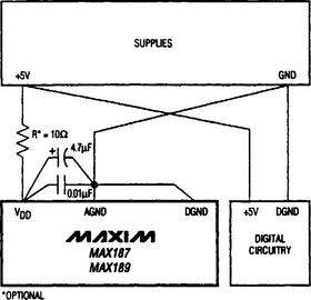
FIGURE 4-18 Recommended power-supply and grounding connections (Maxim New Releases Data Book, 1995, p. 7-59)
Use the single-point or “star” grounding system shown in Fig. 4-18 at the GND terminal. This should be separate from the logic ground. All other analog grounds should be connected to the single-point ground. Connect DGND to the star or single-point ground for further noise reduction. However, no other digital-system ground should be connected to the single-point analog ground. The ground return to the power supply for the single-point ground should be low impedance and as short as possible for noise-free operation.
High-frequency noise in the Vdd power supply can affect the high-speed comparator in the ADC (Fig. 4-1). Bypass this supply to the single-point analog ground with 0.01-μF and 4.7-μF capacitors as shown in Fig. 4-18. Keep capacitor leads short for best supply-noise rejection. If the +5-V supply is very noisy, a 10-ohm resistor can be connected as a lowpass filter to attenuate supply noise as shown in Fig. 4-18.
As is the case with any ADC (and most ICs), use PC boards, not wire-wrap boards, for all final assembly. Keep digital and analog signal lines separated from each other (whenever possible). In any case, do not run analog and digital (especially clock) lines parallel to one another or run digital lines underneath the ADC package.