Simplified Design with Serial-Interface DAC
This chapter is devoted to simplified-design approaches for a typical DAC with three-wire serial interface. All the general design information in Chapters 1 through 3 applies to the examples in this chapter. The circuits in this chapter can be used immediately the way they are or, with alterations in component values, as a basis for simplified design of similar data-converter applications. The chapter concludes with a typical bipolar output circuit.
6.1 General Description of DAC
Figure 6-1 shows the functional block diagram and pin configuration for a DAC (a MAX512/513). This IC contains three 8-bit, voltage-output DACs (DAC A, DAC B, DAC C). Output buffer-amplifiers for DAC A and DAC B provide voltage outputs and are included in the IC to reduce external component count. The output buffer for DAC A can source or sink 5 mA to within 0.5 V of Vdd or Vss. DAC B can can source or sink 0.5 mA to within 0.5 V of Vdd or Vss. DAC C is unbuffered, providing a third voltage output with increased accuracy. The MAX512 operates with a single +5 V ± 10% supply, and the MAX513 operates with a +2.7-V to +3.6-V supply. Both DACs can also operate with split supplies.

FIGURE 6-1 Functional block diagram and pin configuration of MAX512/513 (Maxim New Releases Data Book, 1995, p. 9-7)
The DACs are well suited for portable and battery-operated applications because of ultra-low power consumption and the DIP/SO IC package. Operating supply current is 1 mA, dropping to less than 1 μA at shutdown. Any of the three DACs can be independently shut down. In the shutdown mode, the reference-resistor ladder network of the DAC is disconnected from the reference input, minimizing system power consumption.
The three-wire serial interface has a maximum operating frequency of 5 MHz and is compatible with SPI™, QSPI™, and Microwire™. The serial-input shift register is 16 bits long and consists of 8 bits of DAC input data and 8 bits for DAC selection and shutdown. The DAC registers can be loaded independently or in parallel at the positive edge of ![]() . A latched-logic output is also available for auxiliary control.
. A latched-logic output is also available for auxiliary control.
SPI™ and QSPI™ are trademarks of Motorola. Microwire™ is a trademark of National Semiconductor.
6.2 Data-Converter Operation
Figures 6-2 and 6-3 show the pin descriptions and simplified circuit diagram, respectively. The DACs are “inverted” R–2R ladder networks using complementary switches that convert 8-bit digital inputs into equivalent analog output voltages in proportion to the applied reference voltages. (Compare Fig. 6-3 with the circuits of Figs. 1-1 and 1-2.)
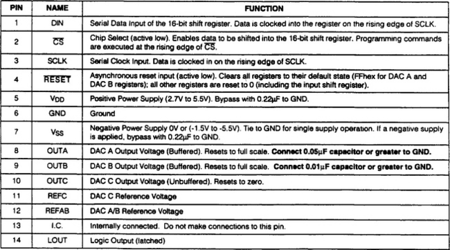

The DACs have two reference inputs (see Fig. 6-1). One reference (REFab) is shared by DAC A and DAC B. The REFc reference is used only by DAC C. These reference inputs allow different full-scale output voltages, and different output polarities, for the DAC pair A/B and DAC C. All three DACs within the IC operate in either single-supply or dual-supply modes, as determined by Vss. If Vss is within approximately −0.5 V of GND, single-supply mode is assumed. If Vss is less than −1.5 V, the DACs are in dual-supply mode.
6.3 Reference Inputs versus DAC Output Range
The voltage at the reference inputs sets the full-scale output of the DACs in the usual manner. The input impedance of the reference inputs is code dependent. The lowest value, about 12 kohms for REFc (8 kohms for REFab), occurs when the digital input code to be converted is 01010101 (which is 55 in hex code). The maximum input impedance (infinity) occurs when the input code is zero.
In the shutdown mode, the selected DAC output is set to zero. The value stored in the DAC register remains unchanged. This removes the load from the reference input to save power. Bringing the DACs out of shutdown restores the DAC output voltage. Because the input resistance at the reference is code dependent, the DAC reference sources should have an output impedance of no more than 5 ohms. The input capacitance at the reference input pins is also code dependent, and typically does not exceed 25 pF.
The reference voltage on REFab can be anywhere between the power-supply limits (or rails). In dual-supply mode, a positive input voltage on REFab should be less than (Vdd — 1.5 V) to avoid saturating the buffer amplifiers. The reference voltage includes the negative supply rail (see Section 6.4). The REFc input accepts positive voltages up to Vdd and should not be forced below ground. The absolute difference between any reference voltage and GND should not exceed 6 V.
6.4 Output Buffer Amplifiers (DAC A/DAC B)
As shown in Fig. 6-1, the DAC A and DAC B voltage outputs are internally buffered. The buffer amplifiers have a rail-to-rail (Vss to Vdd) output-voltage range. In single-supply mode, the DAC outputs A and B are internally divided by two and the buffer is set to a gain of two, eliminating the need for a buffer input-voltage range to the positive-supply rail. In dual-supply mode, the DAC outputs are not attenuated, and the buffer is set to unity gain.
Although only necessary for negative output voltages, the dual-supply mode can be used even if the desired DAC output voltage is positive. Possible errors associated with the divide-by-two attenuator and gain-of-two buffers in the single-supply mode are eliminated in dual-supply mode. However, do not use reference voltages higher than (Vdd – 1.5 V) for dual supply.
The DAC A output amplifier can source and sink up to 5 mA (0.5 mA for DAC B). The amplifier is unity-gain stable with a capacitive load of 0.05 μF (0.01 μF for DAC) or greater. The slew rate is limited by the load capacitor and is typically 0.1 V/μs with a 0.1-μF load (0.01 μF for DAC B). (If you are not familiar with amplifier terms such as slew rate and unity gain, read my Simplified Design of IC Amplifiers (Butterworth–Heinemann, 1996.)
6.5 Unbuffered Output (DAC C)
The output of DAC C is unbuffered and has a typical output impedance of 24 k. The output can be used to drive a high-impedance load, such as an op amp or comparator, and has 35-μs typical settling time to ½ LSB with a single 3-V supply. Use DAC C if a a quick, dynamic response is required.
6.6 Shutdown Mode
When programmed to shutdown mode, the outputs of DAC A and DAC B go into a high-impedance state where virtually no current flows into or out of the buffer amplifiers. The output of DAC C goes to 0 V when shut down. In shutdown, both reference inputs are high impedance (typically 2 M) to conserve current drain from the system reference. As a result, the system reference does not have to be powered down. The logic output (Lout) remains active in shutdown. When coming out of shutdown, the DAC outputs return to the values kept in the registers. The recovery time is equivalent to the DAC settling time.
6.7 Reset
The ![]() input is active low. When asserted (
input is active low. When asserted (![]() = 0), DAC A and DAC B are set to full scale (FF in hex) and active. DAC C is set to zero code (00 in hex) and active. The 16-bit serial register is cleared to 0000 in hex. Lout is reset to zero.
= 0), DAC A and DAC B are set to full scale (FF in hex) and active. DAC C is set to zero code (00 in hex) and active. The 16-bit serial register is cleared to 0000 in hex. Lout is reset to zero.
6.8 Serial Interface
Figures 6-4 and 6-5 show the basic serial-interface timing and input shift-register configuration, respectively. Figures 6-6 and 6-7 show the detailed timing and timing characteristics, respectively. An active-low chip select (![]() ) enables the shift register to receive data bits from the serial data input. Data bits are clocked into the shift register on every rising edge of the serial-clock signal (SCLK). The clock frequency can be as high as 5 MHz.
) enables the shift register to receive data bits from the serial data input. Data bits are clocked into the shift register on every rising edge of the serial-clock signal (SCLK). The clock frequency can be as high as 5 MHz.

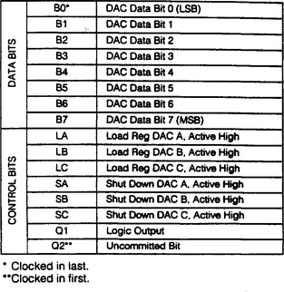
FIGURE 6-5 MAX512/513 input shift-register configuration (Maxim New Releases Data Book, 1995, p. 9-16)
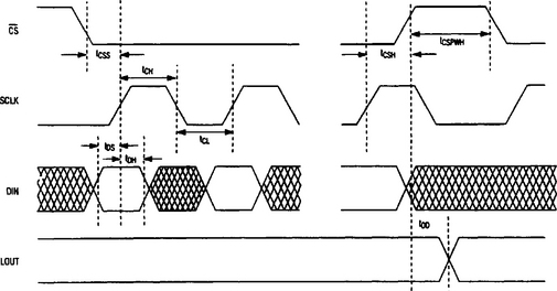

Data bits are sent MSB first and can be transmitted in one 16-bit word. The write cycle can be interrupted at any time when ![]() is kept active (low). This allows two 8-bit-wide transfers, if desired. After all 16 bits are clocked into the input shift register, the rising edge of
is kept active (low). This allows two 8-bit-wide transfers, if desired. After all 16 bits are clocked into the input shift register, the rising edge of ![]() updates the DAC outputs, the shutdown status, and the status of the logic output. Because of their single-buffered structure, DACs cannot be simultaneously updated to different digital values.
updates the DAC outputs, the shutdown status, and the status of the logic output. Because of their single-buffered structure, DACs cannot be simultaneously updated to different digital values.
6.9 Data Format and Control Codes
Figure 6-8 describes the serial-input data format. The 16-bit input word consists of an 8-bit control byte and an 8-bit data byte. The 8-bit control byte is not decoded internally. Every control bit performs one function. Data bits are clocked in starting with Q2 (uncommitted bit), followed by the remaining control bits and the data byte. The LSB of the data byte (B0) is the last bit clocked into the shift register.

Figure 6-9 shows an example of a 16-bit input word. In this example, 128 in decimal (or 80 in hex) is loaded into the DAC registers A and B, which are both active. DAC C is shutdown, and the contents of the DAC C register remain unchanged; LOUT is reset to 0.

6.10 Digital Inputs
The digital inputs are compatible with CMOS logic. Supply current increases slightly when the logic inputs are toggled through the transition zone between (0.3) (Vdd) and (0.7) (Vdd).
6.11 Digital Output
The latched digital output (Lout) has a 1.6-mA source capability with a (Vdd – 0.4 V) output level. With a 1.6-mA sink current, the output voltage at Lout is guaranteed to be no more than 0.4 V. The Lout signal can be used for digital auxiliary control. However, Lout remains fully active during shutdown mode.
6.12 Microprocessor Interfacing
The serial interface is compatible with Microwire™, SPI™, and QSPI™. For SPI™ and QSPI™, clear the CPOL and CPHA bits (CPOL = 0 and CPHA = 0). As described in SPI™ and QSPI™ literature, CPOL = 0 sets the inactive state of the clock to zero, and CPHA = 0 changes data at the falling edge of SCLK. This setting allows both SPI™ and QSPI™ to run at full clock speeds (0.5 MHz and 4 MHz, respectively).
If the microprocessor does not have a serial port, three bits of a parallel port can be used to emulate a serial port by bit manipulation. Operate the serial clock only when necessary to minimize digital feedthrough at the voltage outputs.
6.13 Applications Data
The rest of this chapter describes how the MAX512/513 can be used for specific applications.
6.13.1 DAC with Bipolar Output
Figure 6-10 shows the MAX512/513 used with two Maxim ICL7612A op amps to provide a bipolar output. Figure 6-11 shows the bipolar code table. These op amps have rail-to-rail input common-mode range and rail-to-rail output-voltage swing, making the circuit of Fig. 6-10 ideal for a high output-voltage swing from low supply voltages.

FIGURE 6-10 MAX512/513 used to provide a bipolar output (Maxim New Releases Data Book, 1995, p. 9-20)
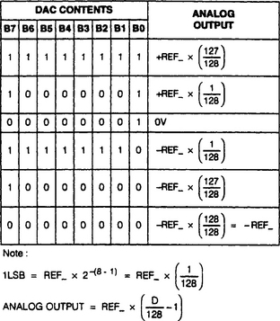
There are two ways to obtain rail-to-rail outputs. First, operate the DACs with a single supply and a positive reference voltage. Second, use dual supplies with a positive or negative voltage at REFab and a positive voltage at REFc. In either case, the op amps require dual supplies. When dual supplies are used, possible errors associated with the divide-by-two attenuator and gain-of-two buffer are eliminated (see Section 6.4).
With dual supplies, DAC A and DAC B can perform four-quadrant multiplication. In the dual-supply mode, REFab ranges from Vss to (Vdd – 1.5 V). Because REFc accepts only positive inputs, DAC C performs only two-quadrant multiplication.
6.13.2 Operating Voltages
Operating voltages for the circuit of Fig. 6-10 depend on the DAC used (MAX512 or MAX513). The MAX512 is fully specified to operation with Vdd = 5 V ± 10% and Vss = GND = 0. The MAX513 is specified for single-supply operation with Vdd ranging from 2.7 V to 3.6 V, covering all commonly used supply voltages in 3-V systems. Both DACs can be used with a negative supply ranging from−1.5 V to 5.5 V. Using a negative supply typically improves zero-code error and settling time.
The two separate reference inputs for the DAC pair A/B and the unbuffered output C allow different full-scale output voltages. If a negative supply is used, the separate reference inputs allow different output polarities. In dual-supply mode, REFab can vary from Vss to (Vdd−1.5 V). In single-supply, the range for REFab is 0 V to Vdd. REFc can range from GND to Vdd. Never force REFc below ground.
Although power-supply sequencing is not critical, make sure that Vss is never more than 0.3 V above ground if a negative supply is used. Also do not apply signals to the digital inputs until the DAC is powered up. If this is not possible, add current-limiting resistors to the digital inputs.
6.13.3 Bypasses and Grounds
In single-supply operation (Vss = GND), GND and Vss should be connected to the highest quality ground available. Bypass Vdd with a 0.1-μF to 0.22-μF capacitor to ground (see Fig. 6-10). For dual-supply operation, bypass Vss with a 0.1-μF to 0.22-μF capacitor to GND. (Note that in Fig. 6-10, ![]() is tied to Vdd, eliminating the need for an external reset signal.)
is tied to Vdd, eliminating the need for an external reset signal.)
The reference inputs can be used without bypassing. However, for the best line-load transient response and noise performance, bypass the reference inputs with 0.1-μF to 4.7-μF capacitors to GND.
6.13.4 PC-Board Layout
As always, careful PC-board layout minimizes crosstalk among DAC output, reference inputs, and digital inputs. Separate analog lines by placing ground traces between the lines. Make sure that high-frequency digital lines are not routed in parallel to analog lines.
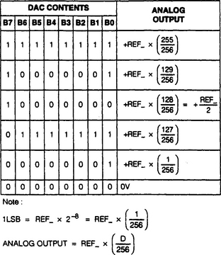
6.13.5 Unipolar Output
Figure 6-12 shows the code table when a unipolar output is required. With unipolar, the output voltage and the reference voltage have the same polarity. Both the MAX512 and MAX513 can be used with a single supply if the reference voltages are positive. With a negative supply, the REFab voltage can vary from Vss to approximately (Vdd – 1.5 V), allowing two-quadrant multiplication.
6.13.6 RF Applications
Figure 6-13 shows how DAC A and DAC B can provide negative bias for two RF amplifiers using gallium-arsenide field-effect transistor, GaAs FETs. Such FETs require that the gate be negatively biased to ensure that there is no drain current. In a typical application, power to the RF amplifiers should not be turned on until the bias voltages provided by the DACs are fully established. The supply should be turned off before the bias voltage is switched off.
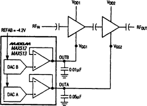
FIGURE 6-13 MAX512/513 used to provide negative bias for two GaAs FET RF amplifiers (Maxim New Releases Data Book, 1995, p. 9-20)
The DAC A and DAC B output can be used for controlling VCOs in mobile radios or cellular phones and to control for varactor and PIN-diode circuits. The unbuffered DAC C provides a span within GND and Vdd and is individually set at REFc. A typical use for DAC C is to set or adjust offset and gain in an RF system.