
Low-Power Data-Acquisition System
This chapter describes an ADC (the MAX192) that contains all major components of a data-acquisition system. Because the ADC requires very low power (1.5-mA operating and 2-μA power-down), the device can provide data acquisition for battery-powered instruments and battery management. The ADC is also well suited for robotic, portable data logging, medical instruments, and any other devices that operate from a single 5-V supply.
9.1 General Description of ADC
Figure 9-1 shows the functional block diagram of the ADC. The IC contains the elements of a 10-bit data-acquisition system that combines an eight-channel multiplexer, high-bandwidth track-and-hold, and serial interface with high conversion speed and ultralow power consumption. The analog inputs are software configurable for single-ended and differential (unipolar-bipolar) operation.

A four-wire serial interface connects directly to SPI™, QSPI™, and Microwire™ devices by means of external logic. A serial strobe output allows direct connection to TMS320-family digital signal processors. SPI and QSPI are trademarks of Motorola. Microwire is a trademark of National Semiconductor.
The IC uses either an internal clock or an external serial-interface clock to perform SAR ADC conversions. The serial interface can operate beyond 4 MHz when the internal clock is used. The IC has an internal 4.096-V reference with a typical drift of ±30 ppm. A reference buffer-amplifier simplifies gain trim. Two sub-LSBs reduce quantization errors.
A hardwired ![]() (shutdown) pin is provided, and there are two software-selectable power-down modes. Accessing the serial interface automatically powers up the device, and the quick turn-on time allows the IC to be shut down between conversions. With powering down between conversions, supply current can be cut to less than 10 μA (at reduced sampling rates).
(shutdown) pin is provided, and there are two software-selectable power-down modes. Accessing the serial interface automatically powers up the device, and the quick turn-on time allows the IC to be shut down between conversions. With powering down between conversions, supply current can be cut to less than 10 μA (at reduced sampling rates).
The device is available in 20-pin DIP and SO packages and in an SSOP that occupies 30% less than an eight-pin DIP.
9.2 Data-Converter Operation
Figure 9-2 shows the pin descriptions for the block diagram of Fig. 9-1. Figure 9-3 shows the IC in a typical operating circuit. As shown, the IC uses a successive-approximation conversion technique and input track-and-hold (T/H) circuitry to convert an analog signal to a 10-bit digital output. A flexible serial interface provides easy interface to microprocessors.


9.2.1 Pseudodifferential Input
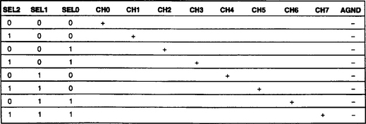
Figure 9-4 shows the sampling architecture of the analog input circuit. In the single-ended mode, IN+ is internally switched to CH0-CH7 and IN– is switched to AGND. In the differential mode, IN+ and IN– are selected from pairs of CH0/CH1, CH2/CH3, CH4/CH5, and CH6/CH7. Figures 9-5 and 9-6 show channel selection for single-ended and differential modes, respectively.
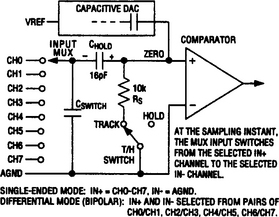
FIGURE 9-4 Sampling architecture of analog input circuit (Maxim New Releases Data Book, 1995, p. 7-67)

In the differential mode, IN– and IN+ are internally switched to either one of the analog inputs. This configuration is pseudodifferential in that only the signal at IN+ is sampled. The return side (IN–) must remain stable within ±0.5 LSB (±0.1 LSB for best results) with respect to AGND during a conversion. To stabilize the return side, connect a 0.1-μF capacitor from AIN– (the selected analog input, respectively) to AGND.
During the acquisition interval, the channel selected as the positive input (IN+) charges capacitor CHOLD. The acquisition interval spans three SCLK cycles and ends on the falling clock (SCLK) edge after the last bit of the input control word has been entered. At the end of the acquisition interval, the T/H switch opens, retaining the charge on CHOLD as a sample of the signal at N +.
The conversion interval begins with the input multiplexer switching CHOLD from the positive input (IN+) to the negative input (IN–). In the single-ended mode, IN– is simply at AGND. This unbalances the ZERO node at the comparator input. The capacitive DAC adjusts during the remainder of the conversion cycle to restore the ZERO node to 0 V (within the resolution limits). This action is equivalent to transferring a charge of 16 pF X (Vin+ – Vin –) from CHOLD to the binary-weighted capacitive DAC, which forms a digital representation of the analog input signal.
9.2.2 Track and Hold
The T/H function enters the tracking mode on the falling clock edge after the fifth bit of the 8-bit control word has been shifted in. The T/H enters the hold mode on the falling clock edge after the eighth bit of the control word has been shifted in.
If the converter is set up for single-ended inputs, IN– is connected to AGND, and the converter samples the +input. If the converter is set up for differential inputs, IN– connects to the –input, and the difference of IN+ – IN– is sampled. At the end of conversion, the positive input connects back to IN+, and CHOLD charges to the input signal.
The time required for the T/H to acquire an input signal is a function of how quickly the input capacitance is charged. If the input-signal source impedance is high, the acquisition time lengthens, and more time must be allowed between conversions. Acquisition time is calculated as follows:
where RIN = 5 k, RS = the source impedance of the input signal, and tAZ is never less than 1.5 μs. Source impedances less than 5 k do not significantly affect the AC performance of the ADC.
9.2.3 Input Bandwidth
The input-tracking circuits have a 4.5-MHz small-signal bandwidth. This makes it possible to use undersampling techniques to digitize high-speed transient events and measure periodic signals with bandwidths that exceed the ADC sampling rate. As discussed in Chapter 4, undersampling can cause aliasing problems, so anti-aliasing filters are recommended. (See the data sheets for the MAX291-MAX297 filters.)
9.2.4 Analog Input Range and Input Protection
Internal protection diodes, which clamp the analog input to Vdd and AGND, allow the channel input pins to swing from AGND – 0.3 V to Vdd + 0.3 V without damage. However, for accurate conversions near full scale, the inputs must not exceed Vdd by more than 50 mV or be lower than AGND by 50 mV.
It is important that if an off-channel analog input exceeds the supplies by more than 50 mV, current will flow through the protection diodes on that input. If this current exceeds 2 mA, the accuracy of the on-channel conversion will be degraded.
The IC can be configured for differential (unipolar or bipolar) or single-ended (unipolar only) inputs, as selected by bits 2 and 3 of the control byte. Figure 9-7 shows the control-byte format. Tables 1 and 2 in Fig. 9-7 refer to Figs. 9-5 and 9-6 in this book.

In the single-ended mode, set the UNI/BIP bit to unipolar. In this mode, analog inputs are internally referenced to AGND with a full-scale input range from 0 V to Vref.
In the differential mode, both unipolar and bipolar settings can be used. Choosing unipolar mode sets the differential input range at 0 V to Vref. The output code is invalid (code 0) when a negative differential input is applied.
The bipolar mode sets the differential input range to ± Vref/2. In the bipolar differential mode, the common-mode input range includes both supply rails. Figure 9-8 shows both unipolar and differential-bipolar ranges.
9.2.5 A Quick-Look Circuit
Figure 9-9 shows a test circuit for evaluating performance of the IC. The IC requires that a control byte be written to Din before each conversion. Tying Din to +5 V feeds in continuous control bytes that trigger single-ended conversions on CH7 (in external clock mode) without powering down between conversions.
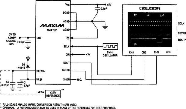
In the external-clock mode, the SSTRB output pulses high for one clock period before the MSB of the conversion result comes out of Dout. Varying the analog input to CH7 should alter the sequence of bits from Dout. A total of 15 clock cycles is required per conversion. All transitions of the SSTRB and Dout outputs occur on the falling edge of SCLK.
9.2.6 Starting a Conversion
One starts a conversion by clocking a control byte (Fig. 9-7) into Din. Each rising edge on SCLK, with ![]() low, clocks a bit from Din into the internal shift register. After
low, clocks a bit from Din into the internal shift register. After ![]() falls, the first arriving logic-1 bit defines the MSB of the control byte. Until this first “start” bit arrives, any number of logic-0 bits can be clocked into Din with no effect.
falls, the first arriving logic-1 bit defines the MSB of the control byte. Until this first “start” bit arrives, any number of logic-0 bits can be clocked into Din with no effect.
For operation with SPI, select the correct clock polarity and sampling edge in the SPI control registers (set CPOL and CPHA to 0). Microwire and SPI both transmit a byte and receive a byte at the same time. Using Fig. 9-3 as an example, the simplest software interface requires only three 8-bit transfers to perform a conversion (one 8-bit transfer to configure the ADC and two more 8-bit transfers to clock out the 12-bit conversion result).
The following sequence shows how the operating circuit of Fig. 9-3 can be set up to provide a conversion. Figure 9-10 shows timing for the sequence. Make certain that the CPU serial interface runs in a master mode so that the CPU generates the serial clock. Choose a clock frequency from 100 kHz to 2 MHz.
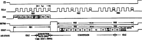
1. Set up the control byte for external clock mode (Fig. 9-7). Call this TB1. TB1 should be of the format: 1XXXXX11 binary, where the Xs denote the particular channel and conversion-mode selected. (The MSB 1 defines the beginning of the control byte; the last two 1s, bit-1 and bit-0, indicate external clock.)
2. Use a general-purpose I/O line on the CPU to pull CS low (to select the MAX192).
3. Transmit TB1 and simultaneously receive a byte. Call this byte RB1 (and ignore it).
4. Transmit a byte of all zeros, and simultaneously receive byte RB2.
5. Transmit a byte of all zeros, and simultaneously receive byte RB3.
As shown in Fig. 9-10, bytes RB2 and RB3 contain the result of the conversion, padded with one leading 0, two sub-LSB bits, and three trailing 0s. The total conversion time is a function of the serial-clock frequency and the amount of dead time between 8-bit transfers. Make sure that the conversion time does not exceed 120 μs.
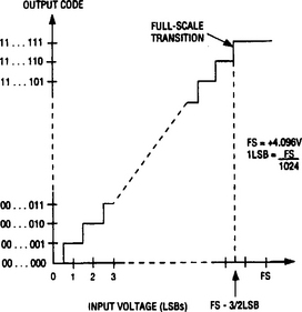
Figures 9-11 and 9-12 show the transfer functions for unipolar and differential-bipolar functions, respectively. For a unipolar input, the digital output is straight binary. For bipolar inputs in the differential mode, the digital output is two’s-complement. In both cases, data bits are clocked out at the falling edge of SCLK in MSB-first format.

9.2.7 Clock Modes
The IC can use either an external serial clock or an internal clock to perform conversion. However, in both clock modes, the external clock shifts data in and out of the IC. The T/H acquires the input signal as the last three bits of the control bytes are clocked in to Din. Bits PD1 and PD0 of the control byte (Fig. 9-7) program the clock mode.
9.2.8 External Clock
Figures 9-13 and 9-14 show the serial-interface and external-clock timing, respectively. In the external-clock mode, the external clock not only shifts data in and out but also drives the ADC conversion process. SSTRB pulses (Fig. 9-2) go high for one clock period after the last bit of the control byte. Successive-approximation bit decisions are made and appear at Dout on each of the next 12 SCLK falling edges (see Fig. 9-10). The first 10 bits are the true data bits, and the last two are sub-LSB bits.


SSTRB and Dout go into a high-impedance state when ![]() goes high, after the next
goes high, after the next ![]() falling edge. SSTRB outputs a logic low.
falling edge. SSTRB outputs a logic low.
The conversion must be complete in a minimum time. If not, the droop on the S/H capacitors might degrade conversion results. As a simplified-design guideline, use the internal-clock mode if the clock period exceeds 10 μs, or if the serial-clock interruptions could cause the conversion interval to exceed 120 μs.
9.2.9 Internal Clock
Figures 9-15 and 9-16 show the internal-clock timing and SSTRB (internal-clock) timing, respectively. In the internal-clock mode, the IC uses the internal clock for processing the conversion steps and the external clock for shifting data in and out. This frees the microprocessor from running the SAR-conversion clock and allows conversion results to be read back at the convenience of the processor at any clock rate from zero to about 10 MHz.

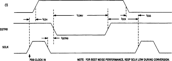
SSTRB goes low at the start of the conversion and then goes high when the conversion is complete. SSTRB is low for a maximum of 10 μs, during which time SCLK should remain low (for best noise performance). An internal register stores data when the conversion is in progress. SCLK clocks the data out of this register at any time after the conversion is complete.
After SSTRB goes high, the next falling clock edge produces the MSB of the conversion at Dout followed by the remaining bits in MSB-first format, as shown in Fig. 9-15. ![]() does not have to be held low after a conversion is started.
does not have to be held low after a conversion is started.
Pulling ![]() high prevents data from being clocked into the IC but does not adversely affect an internal-clock conversion already in progress. When internal-clock mode is selected, SSTRB does not go into a high-impedance state when
high prevents data from being clocked into the IC but does not adversely affect an internal-clock conversion already in progress. When internal-clock mode is selected, SSTRB does not go into a high-impedance state when ![]() goes high.
goes high.
In the internal-clock mode, data can be shifted in and out of the IC at clock rates exceeding 4.0 MHz, provided the minimum acquisition time (tAZ) is kept above 1.5 μs (see Section 9.2.2).
9.2.10 Data Framing
Figure 9-17 shows the serial-interface timing necessary to perform a conversion every 15 SCLK cycles in the external-clock mode. Figure 9-18 shows the timing for conversion every 16 SCLK cycles in external clock. As shown, the falling edge of ![]() does not start a conversion. Instead, the first logic-high clocked into Din is interpreted as a start bit and defines the first bit of the control byte (see Fig. 9-7). A conversion starts on the falling edge of SCLK, after the eighth bit of the control byte (the PD0 bit) is clocked into Din. The start bit is defined as follows:
does not start a conversion. Instead, the first logic-high clocked into Din is interpreted as a start bit and defines the first bit of the control byte (see Fig. 9-7). A conversion starts on the falling edge of SCLK, after the eighth bit of the control byte (the PD0 bit) is clocked into Din. The start bit is defined as follows:

FIGURE 9-17 Serial-interface timing for conversion every 15 cycles (Maxim New Releases Data Book, 1995, p. 7-74)

FIGURE 9-18 Serial-interface timing for conversion every 16 cycles (Maxim New Releases Data Book, 1995, p. 7-74)
The first high bit clocked into Din with ![]() low any time the converter is idle (after Vdd is applied)
low any time the converter is idle (after Vdd is applied)
The first high bit clocked into Din after bit 3 of a conversion in progress is clocked onto the Dout pin.
If a falling edge on ![]() forces a start bit before bit 3 (B3) becomes available, then the current conversion is terminated, and a new conversion is started. As a result, the fastest that the MAX192 can run is 15 clocks per conversion. Many microprocessors require that conversions occur in multiplies of eight SCLK clocks. As a result, 16 clocks per conversion typically is the fastest that a microprocessor can drive the MAX192.
forces a start bit before bit 3 (B3) becomes available, then the current conversion is terminated, and a new conversion is started. As a result, the fastest that the MAX192 can run is 15 clocks per conversion. Many microprocessors require that conversions occur in multiplies of eight SCLK clocks. As a result, 16 clocks per conversion typically is the fastest that a microprocessor can drive the MAX192.
9.3 Applications Information
The rest of this chapter is devoted to applications information for the MAX192.
9.3.1 Power-On Reset
When power is first applied, and if ![]() is not pulled low, internal power-on reset circuits activate the MAX192 in the internal-clock mode. The IC is ready to convert when SSTRB goes high. After the power supplies have been stabilized, the internal reset time is 100 μs, and no conversion should be performed during this phase. SSTRB is high on power-up, and if
is not pulled low, internal power-on reset circuits activate the MAX192 in the internal-clock mode. The IC is ready to convert when SSTRB goes high. After the power supplies have been stabilized, the internal reset time is 100 μs, and no conversion should be performed during this phase. SSTRB is high on power-up, and if ![]() is low, the first logic-1 on Din will be interpreted as a start bit. Until a conversion takes place, Dout shifts out 0s.
is low, the first logic-1 on Din will be interpreted as a start bit. Until a conversion takes place, Dout shifts out 0s.
9.3.2 Reference-Buffer Compensation
In addition to the shutdown function, the SHDN pin selects internal or external compensation. This compensation affects both power-up time and maximum conversion speed. Compensated or not, the minimum clock rate is 100 kHz because of the S/H charge-discharge.
To select external compensation, leave ![]() floating as shown in Fig. 9-3. Also use a 4.7-μF (or larger value) capacitor at Vref as shown. This ensures stability and allows operation of the converter at the full clock speed of 2 MHz. External compensation increases power-up time (see Section 9.3.3).
floating as shown in Fig. 9-3. Also use a 4.7-μF (or larger value) capacitor at Vref as shown. This ensures stability and allows operation of the converter at the full clock speed of 2 MHz. External compensation increases power-up time (see Section 9.3.3).
To select internal compensation, pull ![]() high, and do not use an external capacitor at Vref. Internal compensation allows the shortest power-up time but is available only with an external clock and reduces the maximum clock rate to 400 kHz.
high, and do not use an external capacitor at Vref. Internal compensation allows the shortest power-up time but is available only with an external clock and reduces the maximum clock rate to 400 kHz.
9.3.3 Choosing Power-Down Mode
Figure 9-19 shows how the choice of reference-buffer compensation and power-down mode affects both power-up delay and maximum sample rate. Figure 9-20 shows the software codes for selecting shutdown and clock modes. Figure 9-21 shows the code for hard-wired shutdown and compensation mode. Figure 14c referred to in Fig. 9-19 is Fig. 9-22 in this book.

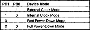
FIGURE 9-20 Software codes for shutdown and clock modes (Maxim New Releases Data Book, 1995, p. 7-76)
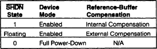
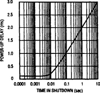
FIGURE 9-22 Typical power-up delay versus time in shutdown (Maxim New Releases Data Book, 1995, p. 7-77)
It is possible to save power by placing a converter in a low-current shutdown or power-down state between conversions. In this converter, you can select (through software) either full power-down or fast power-down via bits 7 and 8 of the Din control byte when ![]() is high, as shown in Figs. 9-7 and 9-20. When
is high, as shown in Figs. 9-7 and 9-20. When ![]() is pulled low, the converter is completely shut down. This is because
is pulled low, the converter is completely shut down. This is because ![]() overrides bits 7 and 8 of the DIN word, as shown in Fig. 9-21. Full power-down mode turns off all chip functions that draw quiescent current, typically reducing Idd to 2 μA.
overrides bits 7 and 8 of the DIN word, as shown in Fig. 9-21. Full power-down mode turns off all chip functions that draw quiescent current, typically reducing Idd to 2 μA.
Fast power-down mode turns off all circuits except the reference. With fast power-down, the supply current is 30 μA. When internal compensation is used with fast power-down, the power-up time is about 5 μs. Keep in mind that in both software shutdown modes (full or fast), the serial interface remains operational, but the ADC does not convert.
Figures 9-23 and 9-24 show the timing diagrams for power-down using external-clock and internal-clock modes, respectively. Figure 9-25 shows the overall power-up sequence for both full and fast power-down modes (FULLPD and FASTPD).


When external compensation is used (4.7-μF capacitor at Vref; see Fig. 9-3), and the capacitor is fully discharged, the power-up time is 20 ms. In fast power-down, the start-up time can be minimized by use of low-leakage capacitors that will not discharge more than ½ LSB during shutdown. (Remember that the capacitor must supply the current into the reference, about 1.5 μA, during shutdown, and must supply transient current at power-up.)
9.3.4 Software Power-Down
As shown in Fig. 9-20, control-byte bits PD0 and PD1 select both the power-down mode and clock mode. When software power-down is used, the ADC continues to operate in the last-specified clock mode until conversion is complete. Then the ADC powers down into a low quiescent state. In the internal-clock mode, the interface remains active, and conversion results can be clocked out during software power-down.
The first logic-1 bit on MDin is interpreted as a start bit. This powers up the IC. After the start bit, the data-input word, or control byte, also determines clock and power-down modes. For example, if the Din word is such that PD1 is a logic-1, then the IC remains powered up. If PD1 is a logic-0, a power-down resumes after one conversion.
9.3.5 Hardware Power-Down
As shown in Fig. 9-21, the ![]() pin selects either internal or external reference compensation and places the IC in full power-down mode. Unlike software power-down, conversion is not complete during hardware power-down. Instead, conversion stops immediately when
pin selects either internal or external reference compensation and places the IC in full power-down mode. Unlike software power-down, conversion is not complete during hardware power-down. Instead, conversion stops immediately when ![]() is brought low.
is brought low.
9.3.6 Power Consumption with Full Power-Down
Figure 9-26 shows the power consumption for one- or eight-channel conversions using full power-down mode and internal reference compensation. A 0.01-μF bypass capacitor (C2 in Fig. 9-3) at REFADJ forms an RC filter with the internal 20-k reference resistor, resulting in a 0.2-ms time constant.
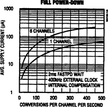
To achieve full 10-bit accuracy, 10 time constants, or 2 ms, are required after power-up. Waiting 2 ms in the fast power-down mode instead of full power-up reduces the power consumption by a factor of 10 or more. This is done by means of the sequence shown in Fig. 9-25.
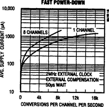
9.3.7 Power Consumption with Fast Power-Down
Figure 9-27 shows the power consumption with external-reference compensation in fast power-down with one and eight channels converted. The external 4.7-μF compensation (Fig. 9-3) requires a 50-μs wait after power-up (accomplished by 75 idle clocks after a dummy conversion). This configuration combines fast multichannel conversion with the lowest power consumption.
9.3.8 Full Power-Down versus Fast Power-Down
As shown in Figs. 9-26 and 9-27, the tradeoff from a simplified-design standpoint is speed versus power. If power consumption is critical, keep the clock (and conversion speed) less than 500 kHz and use full power-down (Fig. 9-26). This allows eight channels of conversion (with more than 400 conversions per channel per second), with an average supply current of 200 μA, or less. If speed is all-important, use fast power-down and an external clock of 2 MHz. This allows eight channels of conversion (with more than 8,000 conversions per channel per second) with about 1,500 μA of supply current.
The full power-down mode can be used in other configurations. An example is a situation in which the IC is inactive for long periods of time but intermittent bursts of high-speed conversions are required. Such a change must be made in software.
9.3.9 External versus Internal Reference
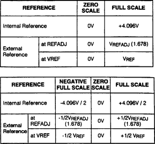
Either an external or the internal reference can be used. Diode D1 (see Fig. 9-3) ensures correct startup. Any standard signal diode can be used for D1. When an external reference is required, the reference can be connected directly at the Vref terminal or at the REFADJ pin. (Either pin can be used because the internally trimmed 2.46-V reference is buffered with a gain of 1.678 to scale an external 2.5-V reference at REFADJ to 4.096 V at Vref, as shown in Fig. 9-1.)
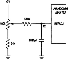
With internal reference, the full-scale range is 4.096 V for unipolar inputs and ±2.048 V for differential bipolar inputs. The internal reference can be adjusted using the circuit of Fig. 9-28. This circuit provides for ±1.5% adjustment of the internal reference.
With external reference, the reference is connected to the input of the internal buffer-amplifier (REFADJ) or to the output at Vref (see Fig. 9-1). The REFADJ input impedance is typically 20 k. The Vref impedance is a minimum of 12 k (for DC).
During conversion, an external reference at Vref must be able to deliver up to 350 μA DC load current and have an output impedance of 10 ohms or less. If the reference has higher output impedance or is noisy, bypass the reference close to the Vref pin with a 4.7-μF capacitor (see Fig. 9-3).
It is not necessary to use an external buffer when the reference is applied to the buffered REFADJ input. However, when using the direct Vref input, disable the internal buffer by tying REFADJ to Vdd.
9.3.10 Transfer Function and Gain Adjust
Figure 9-11 shows the nominal, unipolar I/O transfer function in which a typical circuit is used, such as that of Fig. 9-1. Figure 9-12 shows the differential bipolar I/O transfer function. Code transitions occur halfway between successive integer LSB values. The adjustment circuit for the internal reference (see Fig. 9-28) can be used to set the ADC gain within ±1.5%. This corresponds to ± 15 LSBs of gain-adjustment range.
9.3.11 Layout, Grounding, and Bypassing
Figure 9-29 shows the recommended grounding and bypassing connections. A single-point analog ground (“star” ground point) should be established at AGND separate from the logic ground. All other analog grounds and the DGND should be connected to this ground. No other digital-system grounds should be connected to the single-point analog ground. The ground return to the power supply for this ground should be low impedance and as short as possible for noise-free operation.
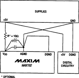
FIGURE 9-29 Recommended grounding and bypassing connections (Maxim New Releases Data Book, 1995, p. 7-79)
High-frequency noise in the Vdd power supply (+5 V) can affect the high-speed comparator in the ADC. If the +5-V supply is very noisy, connect a 10-ohm resistor as shown in Fig. 9-29. The resistor acts as a low-pass filter. Also bypass the +5-V supply to the single-point analog ground with 0.1-μF and 4.7-μF bypass capacitors as shown. Keep the capacitors as close to the IC as possible. The best noise rejection is when the capacitor leads are as short as possible.
As always, for best performance, use PC boards, not wire-wrap boards. Make sure that digital and analog signal lines are separated from each other. Do not run analog and digital (especially clock) lines parallel to one another or digital lines beneath the ADC package.
9.3.12 Interfacing with QSPI
Figure 9-30 shows the interconnections between the MAX192 and a Motorola MC68HC16 for QSPI operation. Figures 9-31 and 9-32 show the assembly code listing. (I have not verified this listing.) Figure 9-33 shows timing for the connections of Fig. 9-30 and the listing of Figs. 9-31 and 9-32.


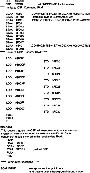
FIGURE 9-32 Continued assembly code listing for QSPI operation (Maxim New Releases Data Book, 1995, p. 7-82)
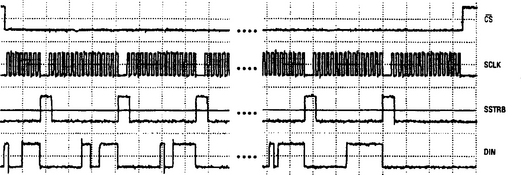
This QSPI configuration can be programmed to perform a conversion on each of the eight channels. The result is stored in memory without taxing the CPU because QSPI incorporates its own microsequencer.
In the external-clock mode, the MAX192 performs a single-ended, unipolar conversion on each of the eight analog-input channels. The first byte clocked into the MAX192 is the control byte, which triggers the first conversion on CHO. The last two bytes clocked into the MAX192 are all 0. These last two bytes clock out the results of the CH7 conversion.
9.3.13 Interfacing with TMS320
Figure 9-34 shows the basic interconnections between the MAX192 and a TMS320. The circuit is operating in the external-clock mode. Use the following steps to initiate a conversion in the MAX192 and to read the results. Figure 9-35 shows the serial-interface timing.
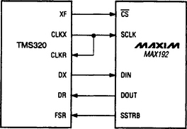

1. Configure the TMS320 with CLKX (transmit clock) as an active-high output clock and CLKR (TMS320 receive clock) as an active-high input clock. CLKX and CLKR of the TMS320 are tied together with the SCLK input of the MAX192.
2. Drive the MAX192 ![]() low via the XF port of the TMS320 to enable data to be clocked into the Din of the MAX192.
low via the XF port of the TMS320 to enable data to be clocked into the Din of the MAX192.
3. Write an 8-bit word (1XXXXX11) to the MAX192 to initiate a conversion and to place the ADC in the external-clock mode. Refer to Fig. 9-7 to select the proper XXXXX bit values for the specific application.
4. Monitor the SSTRB output of the MAX192 through the FSR input of the TMS320. A falling edge on the SSTRB output indicates that the conversion is in progress and data bits are ready to be received from the MAX192. The TMS320 reads in one data bit on each of the next 16 rising edges of SCLK. These data bits represent the 10-bit conversion result and two sub-LSBs, followed by four trailing bits, which should be ignored.
5. Pull ![]() high to disable the MAX192 until the next conversion is initiated.
high to disable the MAX192 until the next conversion is initiated.