
Simplified Design with Parallel-Input DAC
This chapter is devoted to simplified-design approaches for a typical DAC with parallel input. All the general design information in Chapters 1 through 3 applies to the examples in this chapter. The circuits in this chapter can be used immediately the way they are or, with alterations in component values, as a basis for simplified design of similar data-converter applications. The chapter concludes with a typical four-quadrant multiplication circuit.
7.1 General Description of DAC
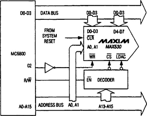
Figure 7-1 shows the functional block diagram and pin configuration for the DAC (a MAX530). The IC is a low-power, 12-bit, voltage-output DAC that uses single +5-V or dual ±5-V supplies. The DAC has an on-chip voltage reference, and an output buffer-amplifier. Operating current is 250 mA from a single +5-V supply, making the DAC useful for portable and battery-powered applications. The available SSOP (shrink small outline package) measures only 0.1 square inch, using less board area than an 8-pin DIP. Twelve-bit resolution is achieved through laser trimming of the DAC, op amp, and references. No further adjustments are required.
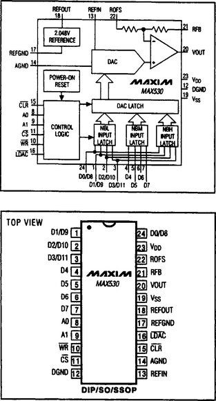
FIGURE 7-1 Functional block diagram and pin configuration of MAX530 (Maxim New Releases Data Book, 1995, p. 9-23)
Internal gain-setting resistors can be used to define a DAC output-voltage range of 0 V to +2.048 V, 0 V to +4.096 V, or ±2.048 V. Four-quadrant multiplication is possible without external resistors or op amps. The parallel logic inputs are double buffered and are compatible with 4-bit, 8-bit, and 16-bit microprocessors.
7.2 Data-Converter Operation
Figures 7-2 and 7-3 show the pin descriptions and simplified circuit diagram, respectively. The MAX530 consists of a parallel-input logic interface, a 12-bit R-2R ladder, a reference, and an op amp. Figure 7-1 shows the control lines and signal flow through the input data latch to the DAC latch and the 2.048-V reference and output op amp.


7.3 R-2R Ladder
As shown in Fig. 7-3, the MAX530 uses an “inverted” R-2R ladder network with a BiCMOS op amp to convert 12-bit digital data into analog voltage levels. In a standard DAC (see Chapters 1 through 3), the REFin pin is the current output and is connected to the summing junction, or virtual ground, of an op amp. This makes the output voltage of a standard DAC the inverse of the reference voltage. In the inverted configuration of the MAX530, the ladder output voltage is of the same polarity as the reference input. This makes the MAX530 suitable for single-supply operation. The BiCMOS op amp is then used to buffer, invert, or amplify the ladder signal, as necessary.
Ladder resistors are nominally 80 k to conserve power and are laser trimmed for gain and linearity. The input impedance at REFin is code dependent. When the DAC register is all 0s, all legs of the ladder are grounded and REFin is open or no-load. Maximum loading (minimum REFin impedance) occurs at code 010101 (or 555 in hex code). Minimum reference input impedance at this code is guaranteed to be not less than 40 k.
The REFin and REFout pins allow the user to choose between driving the R-2R ladder with the on-chip reference or with an external reference. REFin can be below analog ground when dual supplies are used.
7.4 Internal Reference
The on-chip reference is laser trimmed to generate 2.048 V at REFout. The output stage can source and sink current so REFout can settle to the correct voltage quickly in response to code-dependent loading changes. Typical source current is 5 mA, with a sink current of 100 μA.
REFout connects the internal reference to the R-2R DAC ladder at REFin. The R-2R ladder draws 50 μA maximum load current. If any other connection is made to REFout, make certain that the total load current is less than 100 μA to avoid gain errors. A separate REFgnd pin is provided to isolate reference currents from other analog and digital ground currents. When the internal reference is used, REFgnd must be connected to AGND. In applications in which the internal reference is not used, connect REFgnd to Vdd. This shuts down the reference and saves about 100 μA of Vdd supply current.
7.5 Internal Reference Noise
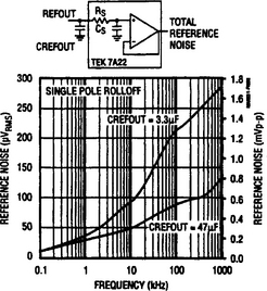
Figure 7-4 shows the noise characteristics of the internal reference. To get the specified noise performance, connect a 33-μF capacitor from REFout to REFgnd. Using smaller capacitance values increases noise. Using values less than 3.3 μF can compromise stability of the reference. For lowest possible noise, insert a buffered RC filter between REFout and REFin.
7.6 Output Buffer-Amplifier
The output buffer-amplifier uses a folded-cascade input stage and a type AB output stage. (Those not familiar with amplifier circuits are invited to read Simplified Design of IC Amplifiers, Butterworth–Heinemann, 1996.) Large-output devices with low series resistance allow the output to swing to ground in single-supply operation. The output buffer is unity-gain stable. Input-offset voltage and supply current are laser trimmed. Settling time is 25 μs to 0.01% of full scale. The output is short-circuit protected and can drive a 2-k load with more than 100 pF of load capacitance.
The output can be placed in unity-gain (G = 1), in a gain of two (G = 2), or in bipolar-output mode using the ROFS and RFB pins (Figs. 7-1 and 7-2). These pins are used to define the DAC output-voltage range of 0 V to +2.048 V, 0 V to +4.096 V, or ±2.048 V, by connecting ROFS to Vout, GND, or REFin, as shown in Fig. 7-5. RFB is always connected to Vout.

7.7 External Reference
If an external reference is required, the manufacturer recommends a MAX873A (2.5 V, ±15-mV initial accuracy, 7-ppm V°C maximum temperature coefficient). In any event, the external reference must be in the range (Vss + 2 V) to (Vdd – 2 V) for dual-supply, unity-gain operation. If single-supply, unity-gain is used, the external reference must be positive and must not exceed (Vdd – 2 V).
As always, the reference voltage determines the DAC full-scale output. Because of the code-dependent nature of reference input impedances (see Section 7.3), a high-quality, low-output-impedance amplifier should be used to drive REFin. (The manufacturer recommends a MAX480.)
7.8 Reset Functions
An internal power-on reset (POR) circuit forces the DAC register to reset to all 0s when Vdd is first applied. The POR pulse is typically 1.3 μs. However, it might take as long as 2 ms for the internal reference to charge the large filter capacitor and settle to the trimmed value.
In addition to POR, a clear (![]() ) pin, when held low, sets the DAC register to all Os.
) pin, when held low, sets the DAC register to all Os. ![]() operates asynchronously and independently from chip select (
operates asynchronously and independently from chip select (![]() ). With the DAC input at all 0s, the op-amp output is at 0 for unity-gain and G = 2 configurations.
). With the DAC input at all 0s, the op-amp output is at 0 for unity-gain and G = 2 configurations.
7.9 Shutdown Mode
Figure 7-6 shows the MAX530 connected for low-current shutdown mode. The MAX530 is designed for low power consumption, and the circuit of Fig. 7-6 requires the minimum shutdown current because of the following. In single-supply mode (Vdd = +5 V, Vss = GND), the initial supply current is typically 160 μA, including the reference, op amp, and DAC. This low current occurs when the power-on reset circuit clears the DAC to all 0s and forces the op-amp output to zero. Under these conditions, there is no internal load on the reference (DAC = 000 in hex, REFin = infinity) and the op amp operates at minimum quiescent current. The ![]() signal resets the MAX530 to these same conditions and can be used to control a power-saving mode when the DAC is not being used by the system.
signal resets the MAX530 to these same conditions and can be used to control a power-saving mode when the DAC is not being used by the system.
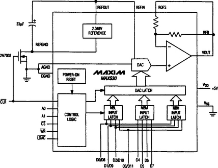
An additional 110 μA of supply current can be saved when the internal reference is not used by connecting REFgnd to Vdd (through ![]() ), as shown in Fig. 7-6. The low on-resistance of the 2N7002 FET turns off the internal resistance. When
), as shown in Fig. 7-6. The low on-resistance of the 2N7002 FET turns off the internal resistance. When ![]() is high, the FET pulls REFgnd to AGND, and both the reference and DAC operate normally. When
is high, the FET pulls REFgnd to AGND, and both the reference and DAC operate normally. When ![]() goes low, REFgnd is pulled up to Vdd and the reference is shut down. At the same time,
goes low, REFgnd is pulled up to Vdd and the reference is shut down. At the same time, ![]() resets the DAC register to all 0s, and the op-amp output goes to 0 V for unity-gain and G = 2 operating modes. This reduces the total single-supply operating current from 250 μA (400 μA max) to typically 40 μA in the shutdown mode.
resets the DAC register to all 0s, and the op-amp output goes to 0 V for unity-gain and G = 2 operating modes. This reduces the total single-supply operating current from 250 μA (400 μA max) to typically 40 μA in the shutdown mode.
A small error voltage is added to the reference output by the reference current flowing through the FET. (The FET on-resistance should be less than 5 ohms.) A typical reference current of 100 μA adds about 0.5 mV to REFout. Because the reference current and on-resistance increase with temperature, the overall temperature coefficient degrades slightly.
As data bits are loaded into the DAC and the output moves above GND, the op-amp quiescent current increases to the nominal value, and the total operating current averages 250 μA. Using dual supplies (±5 V), the op amp is fully biased continuously, and the Vdd supply current is more constant at 250 μA. The Vss current is typically 150 μA.
The MAX530 logic inputs are compatible with TTL and CMOS. However, to get the lowest power dissipation, drive the digital inputs with rail-to-rail CMOS. With TTL logic levels, the power requirement increases by a factor of about 2.
7.10 Parallel Logic Interface
Figures 7-7 and 7-8 show the input addressing scheme and write-cycle timing diagram, respectively. The MAX530 uses 8 data pins and double-buffered logic inputs to load data as 4 + 4 + 4, or 8 + 4. This makes it possible to interface with 4-bit, 8-bit, and 16-bit microprocessors. The 12-bit DAC latch is updated simultaneously through the control signal ![]() . Signals A0, A1,
. Signals A0, A1, ![]() , and
, and ![]() select which input latches to update.
select which input latches to update.
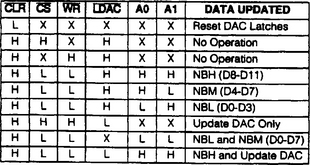
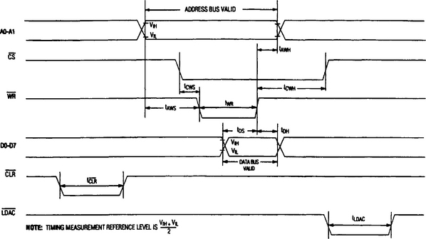
The 12 data bits are broken down into nibbles (NB). NBL is the enable signal for the lowest 4 bits, NBM is the enable for the middle 4 bits, and NBH is the enable for the highest and most important 4 bits.
7.11 4-Bit Microprocessor Interface
Figures 7-9 and 7-10 show the basic connections and timing sequence, respectively, for a 4-bit microprocessor interface. The 4 low bits (D0-D3) are connected in parallel to the other 4 bits (D4-D7) and then to the microprocessor bus. Address lines A0 and A1 enable the input-data latches for high, middle, or low data nibbles. The microprocessor sends ![]() and
and ![]() ) signals to latch in each of three nibbles in three cycles when the data bits are valid.
) signals to latch in each of three nibbles in three cycles when the data bits are valid.

7.12 8-Bit or 16-Bit Microprocessor Interface
Figures 7-11 and 7-12 show the basic connections and timing sequence, respectively, for an 8-bit or 16-bit microprocessor interface, using the ![]() function. Figure 7-13 shows the timing sequence when the
function. Figure 7-13 shows the timing sequence when the ![]() function is not used (held low or 0).
function is not used (held low or 0).

FIGURE 7-11 Basic connections for 8-bit or 16-bit microprocessor interface (Maxim New Releases Data Book, 1995, p. 9-34)
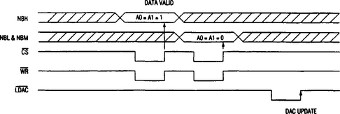
FIGURE 7-12 Timing sequence for 8-bit or 16-bit microprocessor interface using ![]() function (Maxim New Releases Data Book, 1995, p. 9-34)
function (Maxim New Releases Data Book, 1995, p. 9-34)
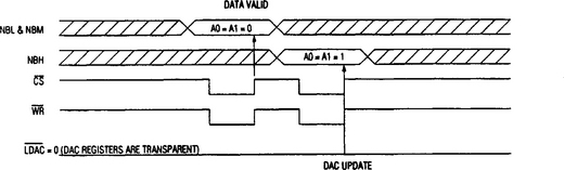
FIGURE 7-13 Timing sequence for 8-bit or 16-bit microprocessor interface with ![]() = 0 (Maxim New Releases Data Book, 1995, p. 9-35)
= 0 (Maxim New Releases Data Book, 1995, p. 9-35)
With ![]() held high, the user can load NBH, or NBL + NBM, in any order, as shown in Fig. 7-12. For the fastest throughput, use the sequence in Fig. 7-13, in which
held high, the user can load NBH, or NBL + NBM, in any order, as shown in Fig. 7-12. For the fastest throughput, use the sequence in Fig. 7-13, in which ![]() is held low. Address lines A0 and A1 are tied together and the DAC is loaded in 2 cycles as 8 + 4. (The DAC latch is transparent in this mode.) Always load NBL and NBM first, followed by NBH.
is held low. Address lines A0 and A1 are tied together and the DAC is loaded in 2 cycles as 8 + 4. (The DAC latch is transparent in this mode.) Always load NBL and NBM first, followed by NBH.
![]() is asynchronous with respect to
is asynchronous with respect to ![]() . If
. If ![]() is brought low before or at the same time
is brought low before or at the same time ![]() goes high,
goes high, ![]() must remain low for at least 50 ns to ensure that the correct data bits are latched. Data bits are latched into the DAC registers on the
must remain low for at least 50 ns to ensure that the correct data bits are latched. Data bits are latched into the DAC registers on the ![]() rising edge.
rising edge.
7.13 Unipolar Operation
Figures 7-14 and 7-15 show the basic connections for unipolar operation. Figures 7-16 and 7-17 show the corresponding unipolar code tables.
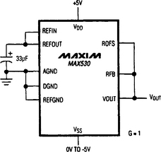
FIGURE 7-14 Basic connections for unipolar operation with 0-V to + 2.048-V output (Maxim New Releases Data Book, 1995, p. 9-35)
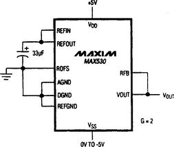
FIGURE 7-15 Basic connections for unipolar operation with 0-V to +4.096-V output (Maxim New Releases Data Book, 1995, p. 9-35)
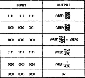
FIGURE 7-16 Unipolar code table for 0-V to +2.048-V output (Maxim New Releases Data Book, 1995, p. 9-36)

FIGURE 7-17 Unipolar code table for 0-V to +4.096-V output (Maxim New Releases Data Book, 1995, p. 9-36)
As shown in Figs. 7-5 and 7-14, the MAX530 is configured for a 0-V to +2.048-V unipolar output when ROFS and RFB are connected to Vout. The IC can operate from either single or dual supplies in this configuration. Figure 7-16 shows the DAC-latch contents (input) versus the analog Vout (output), where 1 LSB = REFin (2-12).
As shown in Figs. 7-5 and 7-15, the MAX530 is configured for a 0-V to +4.096-V unipolar output when ROFS is connected to AGND and RFB is connected to Vout. The IC can operate from either single or dual supplies in this configuration. Figure 7-17 shows the DC-latch contents versus analog Vout, where 1 LSB = (2)(REFin)(2−12) = (REFin)(2−11).
7.14 Bipolar Operation
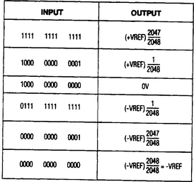
Figures 7-18 and 7-19 show the basic connections and code table, respectively, for bipolar operation. As shown in Figs. 7-5 and 7-18, the MAX530 is configured for −2.048-V to +2.048-V bipolar range when ROFS is connected to REFin and RFB is connected to Vout. Dual supplies (±5 V) must be used in this configuration. Figure 7-19 shows the DAC-latch contents versus analog Vout, where 1 LSB = REFin(2)−11).

7.15 Four-Quadrant Multiplication
Figure 7-20 shows the basic connections for four-quadrant multiplication. This configuration requires that ROFS be connected to REFin, that an offset-dual or two’s-complement code be used, bipolar power supplies be available, and the bipolar analog input at REFin (for multiplication) be in the range of Vss + 2 V to Vdd – 2V
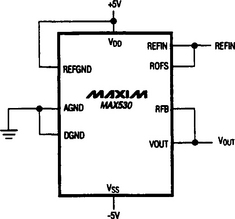
FIGURE 7-20 Basic connections for four-quadrant multiplication (Maxim New Releases Data Book, 1995, p. 9-37)
A 12-bit DAC output is typically (D)(VREFin)(G) where G is the gain (1 or 2) and D is the binary representation of the digital input divided by 212 or 4096. This formula is precise for unipolar operation. However, for bipolar, two’s-complement operation, the MSB is really a polarity bit. No resolution is lost because there are the same number of steps. However, the output voltage has been shifted. For example, 0V to 4.096 V (G = 2) is shifted to a range of −2.048 V to +2.048 V. Keep in mind that when the DAC is used as a four-quadrant multiplier, the scale is skewed. The negative full scale is – VREFin, with the positive full scale at +VREFin – 1 LSB.
7.16 Single-Supply Problems
As in the case of any op amp, there are linearity problems when a single supply is used, and these problems apply to the output op amp of the MAX530. For example, op amp output offset can be positive or negative. There is no major problem when the output offset is positive because this can be corrected (usually by an offset adjustment at the input).
The offset problem becomes aggravated when the offset is negative, and there is only one supply. The output cannot follow in a linear manner when there is no negative supply. In that case, the amplifier output (Vout) remains at ground until the DAC voltage is sufficient to overcome the offset and the offset becomes positive. This results in a stepped transfer function such as shown in Fig. 7-21.

FIGURE 7-21 Stepped-transfer function for single supply (Maxim New Releases Data Book, 1995, p. 9-38)
Linearity normally is measured after one allows for zero error and gain error. However, because the actual value of a negative offset is unknown, the value cannot be accounted for during testing in single-supply operation. In the MAX530, linearity and gain error are measured from code 11 to code 4095. The output-amplifier offset does not affect monotoniticy, and the DACs are guaranteed monotonic starting with code zero. In dual-supply operation, linearity and gain are measured from code 0 to 4095.
7.17 Bypasses, Grounds, and PC-Board Layout
All of the recommendations in Sections 6.13.3 and 6.13.4 apply to the MAX530 (and to most DACs).
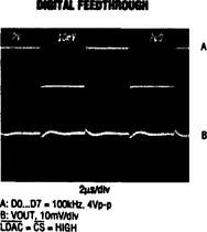
7.18 Digital and Analog Feedthrough
High-speed data at any of the digital-input pins can couple through a DAC and cause internal stray capacitance to appear as noise at the DAC output, even though ![]() and
and ![]() are held high. (This is known as digital feedthrough.) The condition is tested by holding
are held high. (This is known as digital feedthrough.) The condition is tested by holding ![]() and
and ![]() high and toggling the data inputs from all 1s to all 0s. A typical pattern is shown in Fig. 7-22.
high and toggling the data inputs from all 1s to all 0s. A typical pattern is shown in Fig. 7-22.
Because of internal stray capacitance, higher-frequency analog input signals at REFin (for example, for four-quadrant multiplication) can couple to the output, even when the input digital code is all 0s. (This is known as analog feedthrough.) The condition is tested by sweeping REFin and setting CLR to low (which sets the DAC switches to 000 in hex). Typical test results are shown in Fig. 7-23.
