
Chapter 10
Tremendously Talented Transistors
IN THIS CHAPTER
![]() Revolutionizing electronics with the tiny transistor
Revolutionizing electronics with the tiny transistor
![]() Understanding transistor action
Understanding transistor action
![]() Using transistors as teeny-tiny switches
Using transistors as teeny-tiny switches
![]() Giving signals a boost with transistors
Giving signals a boost with transistors
Imagine the world without the amazing electronics building block known as the transistor. Your cellphone would be the size of a washing machine, your laptop wouldn’t fit on your lap (or in a single room), your iPod would be just another pie-in-the-sky idea — and your Apple stock would be worthless.
Transistors are the heart of nearly every electronic device in the world, quietly working away without taking up much space, generating a lot of heat, or breaking down every so often. Generally regarded as the most important technological innovation of the 20th century, transistors were developed as an alternative to the vacuum tube, which drove the development of electronic systems ranging from radio broadcasting to computers but exhibited some undesirable characteristics. The solid-state transistor enabled the miniaturization of electronics, leading to the development of cellphones, iPods, GPS systems, implantable pacemakers — and much more.
In this chapter, you find out what transistors are made of and the secrets of their success. You discover how transistors amplify tiny signals and how to use transistors as microscopic switches. Finally, you observe transistor action firsthand by building a couple of simple transistor circuits.
Transistors: Masters of Switching and Amplifying
Transistors basically do just two things in electronic circuits: switch and amplify. But those two jobs are the key to getting really interesting things done. Here’s why those functions are so important:
Switching: If you can switch electron flow on and off, you have control over the flow, and you can build involved circuits by incorporating lots of switches in the right places.
Consider, for instance, the telephone-switching system: By dialing a 10-digit number, you can connect with any one of millions of people around the world. Or look at the Internet: Switching enables you to access a website hosted in, say, Sheboygan while you’re sitting on a train in, say, London. Other systems that rely on switching are computers, traffic lights, the electric power grid — well, you get the idea. Switching is pretty darn important.
Amplifying: If you can amplify an electrical signal, you can store and transmit tiny signals and boost them when you need them to make something happen.
For instance, radio waves carry tiny audio signals over long distances, and it’s up to the amplifier in your stereo system to magnify the signal so it can move the diaphragm of a speaker so you can hear the sound.
Before the invention of the transistor, vacuum tubes did all the switching and amplifying. In fact, the vacuum tube was widely regarded as the greatest marvel in electricity in the early 20th century. Then, Bardeen, Brattain, and Shockley showed the world that tiny semiconductor transistors could do the same job — only better (and for less money). The trio was awarded the 1956 Nobel Prize in Physics for their invention of the transistor.
Transistors these days are microscopically small, have no moving parts, are reliable, and dissipate a heck of a lot less power than their vacuum-tube predecessors. (However, many audiophiles believe tubes offer superior sound quality compared to solid-state transistor technology.)
The two most common types of transistors are
- Bipolar junction transistors
- Field-effect transistors
Figure 10-1 shows the circuit symbols commonly used for various types of transistors. The sections that follow provide a closer look at bipolar transistors and field-effect transistors.
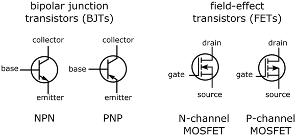
FIGURE 10-1: Circuit symbols for bipolar junction transistors and field-effect transistors, with labeled leads.
Bipolar junction transistors
One of the first transistors to be invented was the bipolar junction transistor (BJT), and BJTs are what most hobbyists use in home-brewed circuits. BJTs consist of two pn-junctions fused together to form a three-layer sandwich-like structure. As Chapter 9 explains, a pn-junction is the boundary between two different types of semiconductors: a P-type semiconductor, which contains positive charge carriers (known as holes), and an N-type semiconductor, which contains negative charge carriers (electrons).
Leads are attached to each section of the transistor, and are labeled the base, collector, and emitter. There are two types of bipolar transistors (see Figure 10-2):
- NPN transistor: A thin piece of P-type semiconductor is sandwiched between two thicker pieces of N-type semiconductor, and leads are attached to each of the three sections.
- PNP transistor: A thin piece of N-type semiconductor is sandwiched between two thicker pieces of P-type semiconductor, and leads are attached to each section.
 Bipolar transistors essentially contain two pn-junctions: the base-emitter junction and the base-collector junction. By controlling the voltage applied to the base-emitter junction, you control how that junction is biased (forward or reverse), ultimately controlling the flow of electrical current through the transistor. (In Chapter 9, I explain that a small positive voltage forward-biases a pn-junction, allowing current to flow, and that a negative voltage reverse-biases a pn-junction, prohibiting current from flowing.)

FIGURE 10-2: Bipolar junction transistors contain two pn-junctions: the base-emitter junction and the base-collector junction.
Field-effect transistors
A field-effect transistor (FET) consists of a channel of N- or P-type semiconductor material through which current can flow, with a different material (laid across a section of the channel) controlling the conductivity of the channel (see Figure 10-3).

FIGURE 10-3: In a field-effect transistor (FET), voltage applied to the gate controls the flow of current through a channel from the source to the drain.
One end of the channel is known as the source, the other end of the channel is called the drain, and the control mechanism is called the gate. By applying a voltage to the gate, you control the flow of current from the source to the drain. Leads are attached to the source, drain, and gate. Some FETs include a fourth lead so you can ground part of the FET to the chassis of the circuit. (But don’t confuse these four-legged creatures with dual-gate MOSFETs, which also have four leads.)
FETs (pronounced “fetts”) come in two flavors — N-channel and P-channel — depending on the type of semiconductor material (N-type or P-type, respectively) through which current flows. There are two major subtypes of FET: MOSFET (metal-oxide-semiconductor FET) and JFET (junction FET). Which is which depends on how the gate is constructed — which results, in turn, in different electrical properties and different uses for each type. The details of gate construction are beyond the scope of this book, but you should be aware of the names of the two major types of FETs.
FETs (particularly MOSFETs) have become much more popular than bipolar transistors for use in integrated circuits (ICs), which I discuss in Chapter 11, where thousands of transistors work together to perform a task. That’s because they’re low-power devices whose structure allows thousands of N- and P-channel MOSFETs to be crammed like sardines on a single piece of silicon (that is, semiconductor material).
 Electrostatic discharge (ESD) can damage FETs. If you purchase FETs, be sure to keep them in an antistatic bag or tube — and leave them there until you’re ready to use them. You can read more about the harmful effects of ESD in Chapter 13.
Recognizing a transistor when you see one
The semiconductor material in a transistor is the size of a grain of sand or even smaller, so manufacturers put these teensy components in a metal or plastic case with leads sticking out so you can connect them in your circuits. You can find literally dozens upon dozens of different shapes and sizes of transistors, some of which are shown in Figure 10-4.
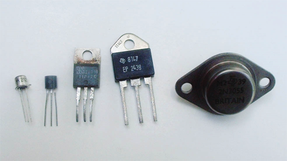
FIGURE 10-4: The drab, dull packaging of the average transistor is just a cover for its exciting, game-changing interior.
The smaller packages generally house signal transistors, which are rated to handle smaller currents. Larger packages contain power transistors, which are designed to handle larger currents. Most signal transistors come in plastic cases, but some precision applications require signal transistors housed in metal cases to reduce the likelihood of stray radio-frequency (RF) interference.
Bipolar transistors typically have three wire leads so you can access the base, collector, and emitter of the transistor. One exception to this is a phototransistor (which I discuss in Chapter 12), which is packaged in a clear case and has just two leads (collector and emitter) — light is used to bias the transistor, so you don’t have to apply a voltage to the base. All FETs have leads for the source, drain, and gate, and some include a fourth lead so you can ground the transistor’s case to the chassis of your circuit, or for the second gate of a dual-gate MOSFET.
To figure out which package lead is which, consult the documentation for the specific transistor. Be careful how you interpret the documentation: Transistor connections are often (though not always) shown from the underside of the case, as if you’ve turned the transistor over and are gazing at it from the bottom.
You absolutely must install transistors the proper way in your circuits. Switching the connections around can damage a transistor and may even damage other circuit components.
Making all kinds of components possible
Transistors can be combined in all sorts of ways to make lots of incredible things happen. Because the semiconductor material that makes up a transistor is so small, it’s possible to create a circuit containing hundreds or thousands of transistors (along with resistors and other components) and plop the entire circuit into a single component that fits easily into the palm of your hand. These amazing creations, known as integrated circuits (ICs), enable you to build really complex circuits with just a few parts. The next chapter takes a look at some of the ICs that are available today as a result of the semiconductor revolution.
Examining How Transistors Work
BJTs and FETs work basically the same way. The voltage you apply to the input (base, for a BJT, or gate, for a FET) determines whether or not current flows through the transistor (from collector to emitter for a BJT, and from source to drain for a FET).
 To get an idea of how a transistor works (specifically, a FET), think of a pipe connecting a source of water to a drain with a controllable valve across a section of the pipe, as shown in Figure 10-5. By controlling whether the valve is fully closed, fully open, or partially open, you control the flow of water from the source to the drain.

FIGURE 10-5: Like a valve, a transistor can be off (no current), fully on (maximum current), or partially on (amount of current depends on how wide the gate is open, so to speak).
You can set up the control mechanism for your valve in two ways. The control mechanism can
- Act like an on/off switch, either fully opening or fully closing with nothing in between.
- Open partially, depending on how much force you exert on it. When it’s partially open, you can adjust the valve a little to allow more or less water to flow from source to drain; small changes in the force you exert on the valve create similar, yet larger, changes in the flow of water. That’s how a transistor acts as an amplifier.
Bipolar transistors work in a similar way: The base acts like the controllable valve in Figure 10-5, controlling the flow of electrons from the emitter to the collector (or, in circuit-speak, the flow of conventional current from the collector to the emitter). By controlling the base, you can turn the transistor fully on or fully off, or you can allow small changes at the base to control large changes in current from collector to emitter.
Using a model to understand transistors
Exactly how a transistor works internally involves technical details about free electrons, moving holes, pn-junctions, and biasing. You don’t have to know all that technical stuff by chapter and verse to use transistors in circuits. Instead, familiarize yourself with a functional model of a transistor, and you’ll know enough to get going.
Figure 10-6 shows a simple model of an NPN transistor on the left, and the circuit symbol for an NPN transistor on the right. The model includes a diode representing the base-emitter junction, and a variable resistance, RCE, between the collector and the emitter. The value of the variable resistance is controlled by the diode in this model. Voltages, currents, and transistor terminals are labeled so you can see how the model corresponds to the actual device.

FIGURE 10-6: A transistor works as a switch or an amplifier, depending on what you input to the base.
Here’s what the voltages and currents represent:
- VBE is the voltage across the base-emitter junction, which is a pn-junction, just like a diode.
- IB (the base current) is the current flowing into the base of the transistor.
- VCE is the voltage from the collector to the emitter. This voltage will vary depending on what is going on at the base.
- IC (the collector current) is the current flowing into the collector.
- IE (the emitter current) is the current flowing out of the emitter. The emitter current is the sum of the collector current and the base current:
 .
.
The transistor has three operating modes, or possibilities for how it operates:
- Cutoff (transistor off): If
 , the diode is off, so
  . This makes the resistance RCE infinite, which means
  . The output of the transistor (collector-to-emitter) is like an open switch: No current is flowing. This mode of operation is called cutoff.
 - Active (transistor partially on): If
 , the diode is on, so base current flows. If IB is small, the resistance RCE is reduced and some collector current, IC, flows. IC is directly proportional to IB, with a current gain, hFE, equal to IC/IB, and the transistor is functioning as a current amplifier — that is, operating in active mode.
 - Saturation (transistor fully on): If
 and IB is increased a lot, the resistance RCE is zero and the maximum possible collector current, IC, flows. The voltage from collector to emitter, VCE, is nearly zero, so the output of the transistor (collector-to-emitter) is like a closed switch: All current that can flow through it is flowing; the transistor is saturated. In this mode, the collector current, IC, is much larger than the base current, IB, and since
 , you can approximate IE as follows:
  .
.
Operating a transistor
When you design a transistor circuit, you choose components that will put the transistor into the right operating mode (cutoff, active, or saturation), depending on what you want the transistor to do. Here’s how:
- Transistor amplifier: If you want to use the transistor as an amplifier (active mode), you select supply voltages and resistors to connect to the transistor so that you forward-bias the base-emitter junction and allow just enough base current to flow — but not so much that the transistor becomes saturated. This selection process is known as biasing the transistor.
- Transistor switch: If you want the transistor to act like an on/off switch, you choose values of supply voltages and resistors so that the base-emitter junction is either nonconducting (the voltage across it is less than 0.7 V) or fully conducting — with nothing in between. When the base-emitter junction is nonconducting, the transistor is in cutoff mode and the switch is off. When the base-emitter junction is fully conducting, the transistor is in saturation mode and the switch is on.
Amplifying Signals with a Transistor
Transistors are commonly used to amplify small signals. (See the sidebar titled “Deciphering electrical signals” for details on what signals are.)
Suppose that you produce an audio signal as the output of one stage of an electronic circuit, and you’d like to amplify it before shipping it off to another stage of electronics, such as a speaker. You use a transistor, as shown in Figure 10-7, to amplify the small up-and-down fluctuations in the audio signal (vin), which you input to the base of the transistor (labeled Q in the schematic). The transistor transforms them into large signal fluctuations (vout), which appear at the output (collector) of the transistor. Then you take the transistor output and apply it to the input of your speakers.

FIGURE 10-7: By strategically positioning a few resistors in a transistor circuit, you can properly bias a transistor and control the gain of this amplifier circuit.
Biasing the transistor so it acts like an amplifier
A transistor must be partially on to work as an amplifier. To put a transistor in this state, you bias it by applying a small voltage to the base. In the example that was shown in Figure 10-7, resistors R1 and R2 are connected to the base of the transistor and configured as a voltage divider (for more about how a voltage divider works, see Chapter 6), dividing the supply voltage, Vsupply. The output of this voltage divider, ![]() , supplies enough voltage to the base to turn the transistor on and allow current to flow through it, biasing the transistor so it’s in the active mode (that is, partially on).
, supplies enough voltage to the base to turn the transistor on and allow current to flow through it, biasing the transistor so it’s in the active mode (that is, partially on).
Capacitor C1 allows only AC to pass through to the transistor, blocking any DC component of the input signal (an effect known as a DC offset), as shown in Figure 10-8. Without that blocking capacitor, any DC offset in the input signal would be added to the bias voltage, potentially saturating the transistor or shutting it off (cutoff) so it no longer acts like an amplifier.

FIGURE 10-8: Blocking capacitor C1 helps maintain the bias of the transistor by filtering out DC offsets in the input signal before the signal gets to the transistor.
Controlling the voltage gain
With the transistor in Figure 10-7 partially on, fluctuations in the base current caused by the AC input signal get amplified by the transistor. Because the current gain, hFE, of any transistor you happen to choose can be somewhat variable (schizophrenic, in fact), you design your amplifier circuit to eliminate any dependency on the flaky current gain. You’ll give up some strength of amplification, but you’ll get stability and predictability in return.
By placing resistors R3 and R4 in the circuit, you can control the voltage gain, or how much the input signal is amplified — without worrying about the exact current gain of the specific transistor at the heart of your circuit. (This is truly amazing stuff!) The AC voltage gain of a transistor circuit with resistors as shown in Figure 10-7 is –R4/R3. The negative sign just means that the input signal is inverted: As the input voltage varies up and then down, the output voltage varies down and then up, as shown by the input and output signal waveforms in Figure 10-7. Before sending the output signal to, say, a speaker, you pass it through another blocking capacitor (C2) to remove any DC offset.
Configuring transistor amplifier circuits
The type of transistor setup I discuss in the preceding section is known as a common-emitter amplifier (so-named because the emitter is tied to common ground); this circuit is just one of many ways to configure transistor circuits for use as amplifiers. You use different configurations to achieve different goals, such as high power gain versus high voltage gain. How the circuit behaves depends on
- How you connect the transistor to the power supplies
- The location of the load
- What other circuit components (such as resistors, capacitors, and other transistors) you add to the circuit
- Where you add other components in the circuit
For instance, you can piggyback two bipolar transistors in a setup known as a Darlington pair to produce multiple stages of amplification. (In the section “Gaining Experience with Transistors,” later in this chapter, you find out how to configure a simple Darlington pair.) Or you can get the same result the easy way: Purchase a three-lead component called a Darlington transistor, which includes a Darlington pair already hooked up.
Designing transistor amplifier circuits is a field of study on its own, and many excellent books have been written on the subject. If you’re interested in learning more about transistors and how to design amplifier circuits using transistors, try getting your hands on a good electronics design book, such as The Art of Electronics, 3rd Edition by Paul Horowitz and Winfield Hill (Cambridge University Press). It isn't cheap, but it’s a classic.
Switching Signals with a Transistor
You can also use a transistor as an electrically operated switch. The base lead of the transistor works like the toggle on a mechanical switch as follows:
- The transistor switch is off when no current flows into the base (in cutoff), and the transistor acts like an open circuit — even if there is a voltage difference from collector to emitter.
- The transistor switch is on when current flows into the base (in saturation), and the transistor acts like a closed switch, fully conducting current from collector to emitter — and out to whatever load you want to turn on.
How do you get this on/off thing to work? Say you use an electronic gadget to scatter chicken feed automatically at dawn. You can use a photodiode, which conducts current when exposed to light, to control the input to a transistor switch that delivers current to your gadget (the load). At night, the photodiode doesn’t generate any current, so the transistor is off. When the sun rises, the photodiode generates current, turning the transistor on and allowing current to flow to your gadget. The gadget then starts scattering chicken feed — keeping the chickens happy while you continue to snooze.
Are you’re wondering why you don’t just supply the current from the photodiode to the gadget? Your gadget might need a larger current than can be supplied by the photodiode. The small photodiode current controls the on/off action of the transistor, which acts like a switch to allow a larger current from a battery to power your gadget.
 One of the reasons transistors are so popular for switching is that they don’t dissipate a lot of power. Remember that power is the product of current and voltage. When a transistor is off, no current flows, so the power dissipated is zero. When a transistor is fully on, VCE is nearly zero, so the power dissipated is nearly zero.
Choosing Transistors
Transistors have become so popular that thousands upon thousands of different transistors are available. So how do you choose one for your circuit, and how do you make sense of all the choices on the market?
If you’re designing a transistor circuit, you need to understand how your circuit will operate under various conditions. What is the maximum amount of collector current your transistor will have to handle? What is the minimum current gain you need to amplify an input signal? How much power could possibly be dissipated in your transistor under extreme operating conditions (for instance, when the transistor is off and the entire power supply voltage may be dropped across the collector-emitter)?
After you understand the ins-and-outs of how your circuit will operate, you can start looking up transistor specifications to find one that meets your needs.
Important transistor ratings
Loads of parameters are used to describe the loads of different transistors, but you need to know only a few parameters to choose the right transistor for your circuit. For bipolar (NPN or PNP) transistors, here’s what you need to know:
- Maximum collector current (ICmax): The maximum DC current that the transistor can handle. When designing a circuit, make sure you use a resistor to limit the collector current so it doesn’t exceed this value.
- DC current gain (hFE or β): The ratio of collector current to base current (that is, IC/IB), which provides an indication of the amplifying capability of the transistor. Typical values are 50 to 200. Because the current gain can vary — even among transistors of the same type — you need to know the guaranteed minimum value of hFE, and that’s what this parameter tells you. The hFE value also varies for different values of IC, so sometimes hFE is given for a specific value of IC, such as 20 mA.
- Maximum collector-to-emitter voltage (VCEmax): The maximum voltage across the collector and emitter; this value is usually at least 30 V. If you’re working with low-power applications such as hobby electronics circuits, don’t worry about this value.
Total power dissipation (Ptotal): The total power that the transistor can dissipate; this value is roughly VCE×ICmax. No need to worry about this rating if you’re using the transistor as a switch because power dissipation is nearly zero anyway. If you’re using the transistor as an amplifier, however, you need to be aware of this rating.
If you think your circuit will approach the total power dissipation value, be sure you attach a heat sink to the transistor.
To determine these characteristics, consult the component's data sheet, which provides technical specifications for the component, on the manufacturer’s website. If you’re building a circuit someone else designed, you don’t have to worry too much about the specs; you can simply use the transistor specified by the designer or consult a cross-reference to find a similar model to substitute.
Identifying transistors
Many bipolar transistors originating in North America are identified by a five- or six-digit code that is part of an industry-standard semiconductor identification system. The first two digits are always 2N for transistors, with the 2 specifying the number of pn-junctions and the N signifying a semiconductor. The remaining three or four digits indicate the specific features of the transistor. However, different manufacturers may use different coding schemes, so your best bet is to consult the appropriate website, catalog, or specification sheet to make sure you’re getting what you need for your circuit.
Many suppliers categorize transistors according to the type of application they are used in, such as low-power, medium-power, high-power, audio (low-noise), or general-purpose. Knowing the category that describes your project can help guide you to choose the right transistor for your particular circuit.
Gaining Experience with Transistors
In this section, you see how tiny transistors control the current in one circuit (at the output of the transistor) using electronic components in another circuit (at the input of the transistor). That’s what transistor action is all about!
Amplifying current
You can use the circuit in Figure 10-9 to demonstrate the amplification capabilities of a transistor.

FIGURE 10-9: A pair of LEDs helps you visualize the amplification capabilities of a transistor.
Here are the parts you need to build the circuit:
- One 9-volt battery with battery clip
- One 2N3904 or BC548 (or any general-purpose) NPN bipolar transistor
- One 470 Ω resistor (yellow-violet-brown)
- One 10 kΩ resistor (brown-black-orange)
- One 1 MΩ potentiometer
- Two LEDs (any size, any color)
- One solderless breadboard and jumpers
Refer to Chapter 2 or Chapter 19 for information on where to get parts.
Using Figure 10-10 as your guide, follow these steps:
Build the circuit using a general-purpose NPN bipolar transistor, such as a 2N3904 or a BC548.
Be careful to connect the base, collector, and emitter leads properly (consult the transistor package or datasheet), and to orient the LEDs correctly (as shown in Chapter 9)
Dial the potentiometer all the way up so that the resistance is 1 MΩ.
You’ll probably see a tiny glow from LED2, but you may not see any light coming from LED1 — although there is a teeny current passing through LED1.
Now slowly dial the pot down and observe the LEDs.
You should see LED2 getting steadily brighter as you dial the pot down. At some point, you'll start to see light from LED1 as well. As you continue to dial the pot down, both LEDs will glow brighter, but LED2 will be clearly much brighter than LED1.
You’re witnessing transistor action: The tiny base current passing through LED1 is amplified by the transistor, which allows a much larger current to flow through LED2. You see a dim glow from LED1 due to the tiny base current, and a bright glow from LED2 due to the stronger collector current. You can measure each current, if you’d like. (See the sidebar “Measuring teeny tiny currents” for a tip on how to measure the small base current.)
With the pot set to 1 MΩ, I measured a base current of 6.7 μA (that’s 0.0000067 A) and a collector current of 0.94 mA. Dividing the collector current by the base current, I found that the current gain of this transistor circuit is 140. With the pot set to 0 Ω, I measured a base current of 0.65 mA and a collector current of 14 mA, for a current gain of approximately 21.5. Pretty intense!
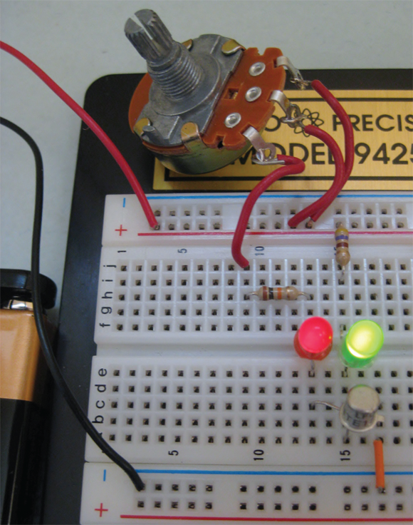
FIGURE 10-10: The small base current barely lights the red LED, while the larger collector current brightly illuminates the green LED.
The switch is on!
The circuit in Figure 10-11 is a touch switch. It uses a pair of NPN transistors to amplify a really teeny base current enough to light the LED. This piggyback configuration of two bipolar transistors, with their collectors connected and the emitter of one feeding into the base of the other, is known as a Darlington pair. (The letter Q is used to label transistors in schematics.)
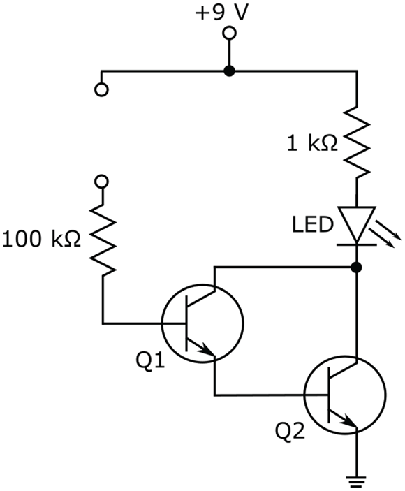
FIGURE 10-11: A Darlington pair can be used as a touch switch.
To test it, set up the circuit as shown in Figure 10-12 using the following parts:
- One 9-volt battery with battery clip
- One 100 kΩ resistor (brown-black-yellow)
- One 1 kΩ resistor (brown-black-red)
- One LED (any size, any color)
- Two 2N3904 or BC548 (or any general-purpose) NPN bipolar transistors
- One solderless breadboard and jumper wires
Close the circuit by placing your finger across the open circuit, as shown in Figure 10-12 (don’t worry, my ten-year-old son didn’t get hurt and you won’t either). Did the LED turn on? When you close the circuit, your skin conducts a teeny tiny current (a few microamps), which is amplified by the pair of transistors, lighting the LED.

FIGURE 10-12: One way to set up the touch switch transistor circuit. You can turn on the LED by placing your finger across the red wire and the 100 kΩ resistor.
If you touch the unconnected lead of the 100 kΩ resistor (without closing the circuit), you may see the LED light up briefly and go out (especially if you shuffle your feet on a carpet first). That’s because you’ve built up a minute amount of charge on your finger, and when you touch the resistor, the charge flows into the base of the first transistor and is amplified enough by the Darlington pair to light the LED. (If the nominal gain, hFE, of your transistors is 100, the total gain of the Darlington pair is ![]() .) After the charge has dissipated, the LED goes out. (Note that if you use an antistatic wrist strap when you touch the resistor, the LED will not light.)
.) After the charge has dissipated, the LED goes out. (Note that if you use an antistatic wrist strap when you touch the resistor, the LED will not light.)