
Chapter 11
Innovating with Integrated Circuits
IN THIS CHAPTER
![]() Corralling components onto a chip
Corralling components onto a chip
![]() Speaking the language of bits
Speaking the language of bits
![]() Thinking logically about gates
Thinking logically about gates
![]() Reading into IC packages
Reading into IC packages
![]() Pondering IC pinouts
Pondering IC pinouts
![]() Boosting signals with op amps
Boosting signals with op amps
![]() Timing, counting, and controlling everything in sight
Timing, counting, and controlling everything in sight
Space exploration, programmable pacemakers, consumer electronics, and much more would be nothing but the idle dreams of creative minds were it not for the integrated circuit (IC). This incredible innovation — really, a series of incredible innovations — makes possible your smartphone, tablet, iPod, and GPS navigation system, as well as newer disruptive technologies, such as 3D printing and autonomous (self-driving) vehicles. Who knows? One day ICs may enable you to 3D-print your own driverless car!
An integrated circuit incorporates anywhere from a few dozen to many billions (yes — billions!) of circuit components into a single device that fits easily into the palm of your hand. Each IC contains an intricate mesh of tiny transistor-based taskmasters, with access to the outside world provided by a finite number of inputs and outputs.
This chapter explores how integrated circuits came to be, identifies the three major IC flavors, and dissects the inner workings of one variety — digital ICs. You get a look at how computers and other digital devices manipulate two distinct voltage levels to process information using special rules known as logic. Next up is an explanation of how to read an IC to understand what the heck it does (because you can’t tell by its cover) and how to connect it for use in circuits. Finally, you get a closer look at three best-selling ICs, what they do, and how you can use them to create your own innovative circuits.
Why ICs?
The integrated circuit (IC) was invented in 1958 (see the sidebar, “The birth of the IC”) to solve the problems inherent in manually assembling mass quantities of tiny transistors. Also called chips, integrated circuits are miniaturized circuits produced on a single piece of semiconductor. A typical integrated circuit contains hundreds of transistors, resistors, diodes, and capacitors; the most advanced ICs contain several billion components. Because of this circuit efficiency, you can build complex circuits with just a few parts. ICs are the building blocks of larger circuits. You string them together to form just about any electronic device you can think up.
Linear, Digital, or Combination Plate?
Over the years, chip makers have come out with lots of different ICs, each of which performs a specific function depending on how the components inside are wired. Many of the integrated circuits you encounter are so popular they have become standardized, and you can find a wealth of information about them online and in books. A lot of different chip makers offer these standardized ICs, and manufacturers and hobbyists the world over buy and use them in various projects. Other special-purpose ICs are designed to accomplish a unique task. More often than not, only a single company sells a particular special-purpose chip.
Whether standardized or special-purpose, you can separate ICs into three main categories: linear (analog), digital, and mixed signal. These terms relate to the kinds of electrical signals (more about those Chapter 10) that work in the circuit:
- Linear (analog) ICs: These ICs contain circuits that process analog signals, which consist of continuously varying voltages and currents. Such circuits are known as analog circuits. Examples of analog ICs are power-management circuits, sensors, amplifiers, and filters.
- Digital ICs: These ICs contain circuits that process digital signals, which are patterns consisting of just two voltage (or current) levels representing binary digital data, for instance, on/off, high/low, or 1/0. (I discuss digital data a bit more in the next section.) Such circuits are known as digital circuits. Some digital ICs, such as microprocessors, contain millions — or billions — of tiny circuits in just a few square millimeters.
- Mixed signal ICs: These ICs contain a combination of analog and digital circuits and are commonly used to convert analog signals to digital signals for use in digital devices. Analog-to-digital converters (ADCs), digital-to-analog converters (DACs), and digital radio processors are examples of mixed signal chips.
Making Decisions with Logic
When you first learned to add numbers, you memorized facts such as “2 + 2 = 4” and “3 + 6 = 9.” Then, when you learned to add multi-digit numbers, you used those simple facts as well as a new one — “carrying” numbers to us older folks, “regrouping” numbers to the younger generation. By applying a few simple addition facts and one simple rule, you can add two large numbers together fairly easily.
 The microprocessor in your computer works in much the same way. It uses lots of teeny digital circuits — known among computer types as digital logic — to process simple functions similar to “2 + 2 = 4.” Then the logic combines the outputs of those functions by applying rules similar to carrying/regrouping to get an answer. By piggybacking lots of these “answers” together in a complex web of circuitry, the microprocessor can perform some complicated mathematical tasks. Deep down inside, though, there’s just a bunch of logic applying simple little rules.
In this section, you get a look at how digital logic circuits work.
Beginning with bits
When you add two digits together, you have ten choices for each digit (0 through 9) because that’s how our numbering system (known as a base 10, or decimal, system) works. When a computer adds two digits together, it uses only two possible digits: 0 and 1 (this is known as a base 2 or binary system). Because there are only two, these digits are known as binary digits, or bits. Bits can be strung together to represent letters or numbers — for instance, the bit string 1101 represents the number 13. The sidebar “Adding bits of numbers” offers a glimpse of how this process works.
In addition to representing numbers and letters, bits can be used also to carry information. As information carriers, data bits are versatile. They can represent many two-state (binary) things: a screen’s pixel is either on or off; a CTRL key is either up or down; a laser pit is either present or absent on a DVD surface; an ATM transaction is either authorized or not; and much more. By assigning logical values of 1 and 0 to a particular on/off choice, you can use bits to carry information about physical events — and allow that information to control other things by processing the bits in a digital circuit.
Logical 1 and logical 0 are also referred to as true and false, or high and low. But what exactly are these ones and zeros in a digital circuit? They are simply high or low currents or voltages that are controlled and processed by transistors. (In Chapter 10, I discuss how transistors work and how they can be used as on/off switches.) Common voltage levels used to represent digital data are 0 volts for logical 0 (low), and (often) 5 volts for logical 1 (high).
 A byte, which you’ve probably heard about quite a bit, is a grouping of eight bits used as a basic unit of information for storage in computer systems. Computer memory, such as random access memory (RAM), and storage devices such as CDs and flash drives, use bytes to organize gobs of data. Just as banks pack 40 quarters into a quarter roll, 50 dimes into a dime roll, and so forth to simplify the process of supplying merchants with change for their cash registers, so computer systems pack data bits together in bytes to simplify the storage of information.
Processing data with gates
Logic gates, or simply gates, are tiny digital circuits that accept one or more data bits as inputs and produce a single output bit whose value (1 or 0) is based on a specific rule. In the same way that different arithmetic operators produce different outputs for the same two inputs (for instance, three plus two produces five, while three minus two produces one), different types of logic gates produce different outputs for the same inputs:
- NOT gate (inverter): This single-input gate produces an output that inverts the input. An input of 1 generates an output of 0, and an input of 0 generates an output of 1. A more common name for a NOT gate is an inverter.
- AND gate: The output is 1 only if both inputs are 1. If either input is 0, the output is 0. A standard AND gate has two inputs, but you can also find three-, four-, and eight-input AND gates. For those gates, the output is 1 only if all inputs are 1.
- NAND gate: This function behaves like an AND gate followed by an inverter (hence the NAND, which means NOT AND). It produces an output of 0 only if all of its inputs are 1. If any input is 0, the output is 1.
- OR gate: The output is 1 if at least one of its inputs is 1. It produces an output of 0 only if both inputs are 0. A standard OR gate has two inputs, but three- and four-input OR gates are also available. For these gates, an output of 0 is generated only when all inputs are 0; if one or more inputs is 1, the output is 1.
- NOR gate: This behaves like an OR gate followed by a NOT gate. It produces an output of 0 if one or more of its inputs are 1, and generates an output of 1 only if all inputs are 0.
- XOR gate: The exclusive OR gate produces an output of 1 if either one — but not both — of the inputs is 1; otherwise, it produces an output of 0. All XOR gates have two inputs, but multiple XOR gates can be cascaded together to create the effect of XORing multiple inputs.
- XNOR gate: The exclusive NOR gate produces an output of 0 if either one — but not both — of the inputs is 1. All XNOR gates have two inputs.
Figure 11-1 shows the circuit symbols for these common logic gates.
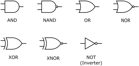
FIGURE 11-1: Circuit symbols for logic gates.
Most logic gates are built using diodes and transistors, which I discuss in Chapters 9 and 10. Inside each logic gate is a circuit that arranges these components in just the right way, so that when you apply input voltages (or currents) representing a specific combination of input bits, you get an output voltage (or current) that represents the appropriate output bit. The circuitry is built into a single chip with leads, known as pins, providing access to the inputs, outputs, and power connections in the circuit.
You usually find multiple logic gates sold in integrated circuits, such as an IC containing four two-input NAND gates (called a quad 2-input NAND gate), as shown in Figure 11-2. The package sports pins that connect to each gate’s inputs and output, as well as other pins that connect a power supply to the circuitry. Look on the website of the IC’s manufacturer for a datasheet that tells you which pins are inputs, outputs, V+ (voltage), and ground. (A datasheet is like a user’s manual; it provides technical specifications and performance information about the chip.)
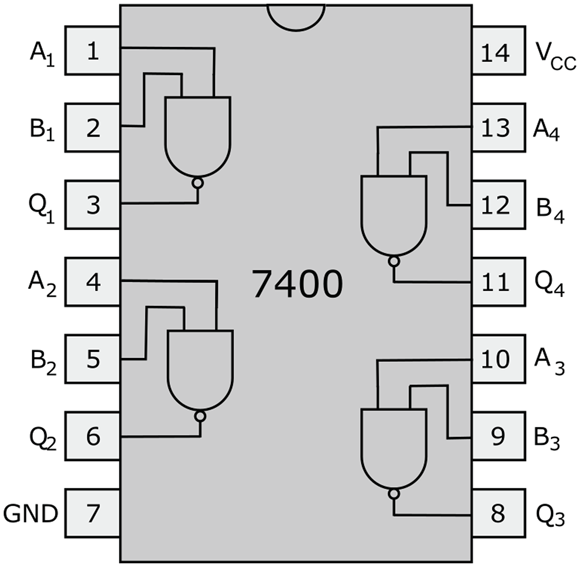
FIGURE 11-2: Functional diagram of the industry-standard 7400 quad 2-input NAND gate IC.
You may see labels in addition to V+ for the positive power supply pin on an IC. Different chip manufacturers use different conventions, but it’s common to see VDD used in CMOS chips and VCC used in TTL chips (see Figure 11-2). Refer to the sidebar “Meet the logic families” for details on CMOS and TTL.
 Make sure that the part you buy has the number of inputs that you need for your project. Remember that you can buy logic gates with more than two inputs. For example, you can find a 3-input NAND gate from most electronics suppliers.
By combining just NAND gates or just NOR gates in just the right way, you can create any of the other logical functions. That’s why NAND and NOR gates are sometimes called universal gates. Chip makers typically build digital circuits using just NAND gates so that they can focus their research and development efforts on improving the process and design of just one basic logic gate.
Simplifying gates with truth tables
Tracking all the 0 and 1 inputs to logic gates and the outputs they produce can get a bit confusing — especially for gates with more than two inputs — so designers use a tool called a truth table to keep things organized. This table lists all the possible combinations of inputs and corresponding outputs for a given logical function.
Figure 11-3 shows the truth tables for the NOT (inverter), AND, NAND, OR, NOR, XOR, and XNOR logic gates, along with labeled symbols for each gate. Each row in the truth table represents a logic statement. For instance, the second row in the NAND truth table is really telling you the following:
You can use truth tables also for other digital circuits, such as a half-adder circuit, which is designed to add two bits and produce an output consisting of a sum bit and a carry bit. For instance, for the binary equation 1 + 1 = 10, the sum bit is 0 and the carry bit is 1. The truth table for the half adder is shown in Figure 11-4.
If you look at the carry-bit column in the truth table for the half adder, you may notice that it looks just like the output for the two-input AND gate shown in Figure 11-3: That is, the carry bit is the same as A AND B, where A and B are the two input bits. Similarly, the sum bit is the same as A XOR B. What’s the significance of this? You can build a half adder using an AND gate and an XOR gate. You feed the input bits into both gates, and use the AND gate to generate the carry bit and the XOR gate to generate the sum bit. (See Figure 11-5.)
Creating logical components
By connecting several adders together in just the right way, you can create a larger digital circuit that takes two multi-bit inputs, such as 10110110 and 00110011, and produces their sum, 11101001. (In decimal notation, that sum is 182+51=233.)
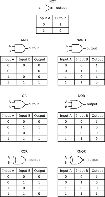
FIGURE 11-3: Truth tables tell you the outputs of a logic gate for each combination of inputs.

FIGURE 11-4: The truth table for the half-adder circuit.

FIGURE 11-5: The half-adder circuit consists of an AND gate and an XOR gate.
You can create loads of other complex functions by combining multiple AND, OR, and NOT gates. It’s all a matter of which gates you use and how you interconnect them. Think about forming words from letters. With just 26 different choices, you can create millions of words. Likewise, you can create circuits that perform math functions (such as adders, multipliers, and many others) by connecting a whole bunch of gates in the right combination.
Over the years, digital circuit designers have perfected the design of adders and other commonly used digital circuits, figuring out clever ways to speed up the computation time, reduce power dissipation, and ensure that the results are accurate, even under harsh circuit conditions such as extreme temperatures. Tried-and-true digital circuit designs are commonly turned into standardized IC product offerings — so you and other circuit builders don’t have to re-create the wheel over and over again.
Using ICs
Integrated circuits are nothing like discrete components — such as individual resistors, capacitors, and transistors — which have two or more leads connected directly to the component inside the package. The miniature prebuilt components inside an IC are already interconnected in one big happy circuit, ready to perform a specific task. You just have to add a few ingredients — say, power and one or more input signals — and the IC will do its thing. Sounds simple, right? Well, it is. You just have to know how to read IC packages — because they all look like black multilegged critters — so you know how to make the right connections.
Identifying ICs with part numbers
Every IC has a unique code, such as 7400 or 4017, to identify the type of device — really, the circuit — that’s inside. You can use this code, also known as a part number, to look up specifications and parameters about an IC in an online resource. The code is printed on the top of the chip.
Many ICs also contain other information, including the manufacturer’s catalog number and maybe even a code that represents when the chip was made. Don’t confuse the date code or catalog number with the part number used to identify the device. Manufacturers don’t have a universal standard for how they stamp the date code on their integrated circuits, so you may have to do some detective work to pick out the actual part number of the IC.
Packaging is everything
Great things really do come in small packages. Many ICs that can fit in the palm of your hand contain incredibly complex circuitry; for example, an entire AM/FM radio circuit (minus the battery and antenna) fits in an IC package the size of a nickel. The actual circuit is so small that manufacturers have to mount it onto a reasonable-size plastic or ceramic package so humans can use it. During the process of chip assembly, leads are attached to the appropriate circuit access points and fed out of the package enclosure so you and others like you can get current flowing to, through, and from the circuit inside.
Many ICs used in hobby electronics projects are assembled into dual in-line packages (DIPs), such as the ones in Figure 11-6. DIPs (sometimes called DILs) are rectangular-shaped plastic or ceramic packages with two parallel rows of leads, called pins, down either side. DIPs contain between 4 and 64 pins, but the most common sizes are 8-, 14-, and 16-pin.
DIPs are designed to be through-hole mounted onto a printed circuit board (PCB), with the pins extending through holes in the board and soldered on the other side. You can solder DIP pins directly onto a circuit board or use sockets designed to hold the chip without bending the pins. You solder the socket connections into your circuit, and then insert the chip into the socket. DIPs also fit nicely into the contact holes of solderless breadboards (which I cover in Chapter 15), making it easy to prototype a circuit.
FIGURE 11-6: A popular form of integrated circuit is the dual in-line package (DIP).
ICs used in mass-produced products are generally more complex and require a higher number of pins than DIPs can provide, so manufacturers have developed (and continue to develop) clever ways of packaging ICs and connecting them to printed circuit boards. To save space on the board (known as real estate), most ICs today are mounted directly to metal connections built onto the PCBs. This is known as surface-mount technology (SMT), and many IC packages are specially designed to be used this way. One such surface-mount IC package is the small-outline integrated circuit (SOIC), which looks like a shorter, narrower DIP with bent leads (called gull wing leads).
SMT packaging has become so widely adopted that it is often difficult to find certain ICs sold in a DIP package. If you want to use a surface-mount IC in a solderless breadboard (because you may not be able to find the DIP variety), look for special DIP adapter modules that convert various surface-mount IC packages to pin-compatible DIP packages you can plug directly into your breadboard. (Enter “DIP adapter” into your favorite Internet search engine to get a list of suppliers of such devices.)
 Some ICs are very sensitive to static electricity (which I discuss in Chapter 13), so when you store your ICs, be sure to enclose them in special conductive foam (sold by most electronics suppliers). And before handling an IC, make sure you wear an antistatic wrist strap or discharge yourself by touching a conductive material that is connected to earth ground (such as the grounded metal case of your home computer) so that you don’t zap your IC and wonder why it’s not working. (Don’t count on the metal pipes in your house to provide a conduit for static charge dissipation. Many home plumbing systems use plastic pipes along the way, so the metal pipes you see in your house aren’t necessarily electrically connected to the earth.)
Probing IC pinouts
The pins on an IC package provide connections to the tiny integrated circuits inside, but alas, the pins are not labeled on the package so you have to rely on the datasheet for the particular IC to make the proper connections. Among other things, the datasheet provides you with the IC’s pinout, which describes the function of each pin.
Use a search engine, such as Google or Yahoo!, to find datasheets for most common (and many uncommon) ICs.
To determine which pin is which, you look down on the top of the IC (not up at the little critter’s underbelly) for the clocking mark, which is usually a small notch in the packaging but might instead be a little dimple or a white or colored stripe. (Some ICs have multiple marks.) By convention, the pins on an IC are numbered counterclockwise, starting with the upper-left pin closest to the clocking mark. So, for example, with the clocking notch orienting the chip at the 12 o’clock position, the pins of a 14-pin IC are numbered 1 through 7 down the left side and 8 through 14 up the right side, as shown in Figure 11-7.

FIGURE 11-7: IC pin numbering runs counterclockwise from the upper left.
Don’t assume that all ICs with the same number of pins have the same pinouts (arrangement of external connections — in this case, pins), or even that they use the same pins for power connections. And never — never! — make random connections to IC pins, under the misguided notion that you can explore different connections until you get the IC to work. That’s a sure-fire way to destroy a poor, defenseless circuit.
Many circuit diagrams (schematics) indicate the connections to integrated circuits by showing an outline of the IC with numbers beside each pin. The numbers correspond to the counterclockwise sequence of the device’s pins, as viewed from the top. (Remember, you start with 1 in the upper left and count up as you go counterclockwise around the chip.) You can use these kinds of diagrams to easily wire an IC because you don’t need to look up the device in a book or a datasheet. Just make sure that you follow the schematic and that you count the pins properly.
If a schematic lacks pin numbers, you need to find a copy of the pinout diagram. For standard ICs, you can find these diagrams online; for nonstandard ICs, you have to visit the manufacturer’s website to get the datasheet.
Relying on IC datasheets
IC datasheets are like owner’s manuals, providing detailed information about the insides, outsides, and recommended use of an integrated circuit. They are created by the IC manufacturer and are usually several pages long. Typical information contained in a datasheet includes
- Manufacturer’s name
- IC name and part number
- Available packaging formats (for instance, 14-pin DIP) and photos of each format
- Dimensions and pinout diagrams
- Brief functional description
- Minimum/maximum ratings (such as power-supply voltages, currents, power, and temperature)
- Recommended operating conditions
- Input/output waveforms (showing how the chip changes an input signal)
Many datasheets include sample circuit diagrams, illustrating how to use the IC in a complete circuit. You can get lots of guidance and good ideas from IC datasheets. Sometimes it really pays to read the owner’s manual!
Manufacturers often publish application notes for their integrated circuits. An application note (often called an app note) is a multipage document that explains in greater detail than the datasheet how to use the IC in an application — a circuit designed for a specific practical task.
Using Your Logic
In this section, you find out firsthand how to make the right connections to a NAND logic gate IC, and you watch the output change as you fiddle around with various combinations of inputs. Then you find out how to create another type of logic gate, an OR gate, by combining NAND gates in just the right way.
Here are the parts you need to build the two circuits in this section:
- Four 1.5-volt AA batteries
- One four-battery holder (for AA batteries) with battery clip
- One 74C00 or 74HC00 quad 2-input NAND gate IC
- Four 10 kΩ resistors (brown-black-orange)
- Two 470 Ω resistors (yellow-violet-brown)
- Four single-pole, double-throw (SPDT) switches
- Two LEDs (any size, any color)
- One solderless breadboard and assorted jumper wires
The 74C00 and 74HC00 are CMOS chips (see the sidebar “Meet the logic families,” earlier in this chapter). You may use a different 2-input NAND, as long as you check the pinout and power supply requirements. For instance, the 4011 is another CMOS 2-input NAND gate, but it has a different pinout from the 74HC00 IC. The 7400 IC is a TTL 2-input NAND chip with the same pinout as the 74HC00 IC, but it requires a fairly steady 5-volt power supply, so you'll need to use a voltage regulator, such as the LM7805, along with a couple of capacitors. You supply 9 volts to the LM7805, and it outputs a steady 5 volts that you can use to power the 7400 IC.
Seeing the light at the end of the NAND gate
The circuit in Figure 11-8 uses an LED to indicate the high (1) or low (0) state of the output of a two-input NAND gate.

FIGURE 11-8: Use an LED to show the output of a NAND logic gate.
Set up the circuit using Figure 11-9 as a guide and noting the following important information:
- The 74HC00 IC is a high-speed CMOS chip that is sensitive to static, so be sure to review the precautions outlined in Chapter 13 to avoid damaging the chip, and insert the IC last — but before you apply power — when you build the circuit, as suggested in Chapter 15.
- You use only one side of each SPDT switch in this circuit so that each switch functions as an on/off switch (refer to Chapter 4 for details). You connect the middle terminal and one end terminal to your circuit and leave the other end terminal unconnected.
Remember that the output of a NAND (NOT AND) gate is high whenever either or both inputs are low, and the output of a NAND gate is low only when both inputs are high. High is defined by the positive power supply (6 V) and low is 0 V.

FIGURE 11-9: With SW1 (top switch) on (slider right) and SW2 (bottom switch) off (slider left), the LED lights up to show that 1 NAND 0 = 1. (Pin number labels have been added.)
When you close one of the switches, you make that input high because you connect the positive power-supply voltage to the input. When you open one of the switches, you make that input low because it’s connected through a resistor to ground (0 V).
Test the functionality of the NAND gate by trying all four combinations of open and closed switches, filling in the chart given here (which is essentially a truth table).
Input 1 |
Input 2 |
Output (High = LED on; Low = LED off) |
Low (SW1 open) |
Low (SW2 open) |
|
Low (SW1 open) |
High (SW2 closed) |
|
High (SW1 closed) |
Low (SW2 open) |
|
High (SW1 closed) |
High (SW2 closed) |
Did you see the LED light up when either or both switches were open? Did the LED turn off when both switches were closed? Be sure to tell the truth!
Turning three NAND gates into an OR gate
You can combine several NAND gates to create any other logical function. In the circuit in Figure 11-10, three NAND gates are combined to create an OR gate. The inputs to the OR gate are controlled by switches SW3 and SW4. The output of the OR gate is indicated by the on/off state of the LED.
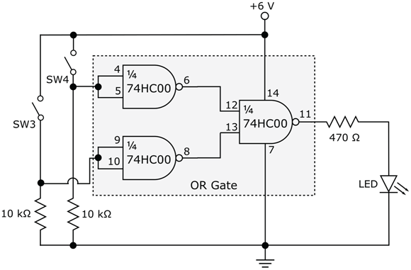
FIGURE 11-10: Three NAND gates configured to create an OR gate.
Each of the two NAND gates on the left functions as a NOT gate (or inverter). Each NAND gate ties the inputs together so that a low input produces a high output, and a high input produces a low output. The NAND gate on the right produces a high output when either or both of its inputs are low, which happens when either or both switches (SW3 and SW4) are closed. The bottom line is that if either or both switches are closed, the output of the circuit is high. That’s an OR gate!
Set up the circuit, being careful to avoid static. You can use the remaining three NAND gates on the 74HC00 IC that you used to build the circuit in Figure 11-9. Figure 11-11 shows the circuits in Figure 11-8 and 11-10 set up together using a single 74HC00. Try not to get your wires crossed!
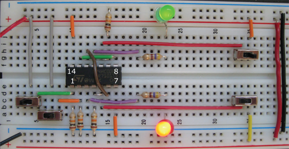
FIGURE 11-11: Using the 74HC00 to demonstrate both a single NAND gate and an OR gate consisting of three NAND gates. (Labels for the four corner pins have been added.)
Test the functionality by opening and closing the switches. The LED should turn on when either or both switches are closed.
Hanging Out with Some Popular ICs
You can find a seemingly endless supply of integrated circuits on the market today, but two in particular are known far and wide for their outstanding versatility and ease of use: the operational amplifier (really a class of ICs) and the 555 timer. It pays to get to know these two circuits fairly well if you intend to get even remotely serious about developing your electronics habit.
In this section, I describe these two popular ICs and one additional IC, the 4017 CMOS decade counter. You encounter the 555 timer IC and the 4017 decade counter IC in projects in Chapter 17, so the upcoming sections provide a quick rundown on how they work.
Operational amplifiers
The most popular type of linear (analog) IC is undoubtedly the operational amplifier, nicknamed the op amp, which is designed to add muscle to (that is, amplify) a weak signal. An op amp contains several transistors, resistors, and capacitors, and offers more robust performance than a single transistor. For example, an op amp can provide uniform amplification over a much wider range of frequencies (bandwidth) than can a single-transistor amplifier.
Most op amps come in 8-pin DIPs (as shown in Figure 11-12), and include two input pins (pin 2, known as the inverting input, and pin 3, known as the non-inverting input) and one output pin (pin 6). An op amp is one type of differential amplifier: The circuitry inside the op amp produces an output signal that is a multiple of the difference between the signals applied to the two inputs. Used a certain way, this setup can help eliminate noise (unwanted voltages) in the input signal by subtracting it out of what’s amplified.
You can configure an op amp to multiply an input signal by a known gain factor that is determined by external resistors. One such configuration, known as an inverting amplifier, is shown in Figure 11-13.
The values of the resistors connected to the op amp determine the gain of the inverting amplifier circuit:
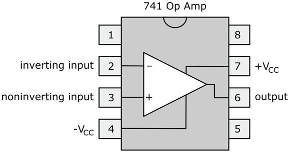
FIGURE 11-12: Pinout of a standard 8-pin op amp, such as the LM741.

FIGURE 11-13: An inverting op-amp circuit provides uniform gain over a wide range of frequencies.
The negative sign indicates that the input signal is flipped, or inverted, to produce the output signal. Say, for instance, that the value of R2 is 10 kΩ and that of R1 is 1 kΩ. The gain is –10. With a gain of –10, a 1 V input signal (peak value) produces an inverted 10 V (peak) output signal.
To use the inverting amplifier, you just apply a signal (for instance, the output of a microphone) between the input pins. The signal, amplified several times, then appears at the output, where it can drive a component, such as a speaker.
Most op amps require both positive and negative supply voltages. A positive supply voltage, VCC, in the range of 8 to 12 V (connected to pin 7) and a negative supply voltage, –VCC, in the range of –8 to –12 V (connected to pin 4) works. (If you’re looking for some light reading, you can find application notes on how to operate such dual-supply op amps using a single power supply.)
Gobs of different op amps are available at prices ranging from just a few cents for standard op-amp ICs, such as the LM741 general-purpose op amp, to $10 or more for high-performance op amps.
IC time machine: the 555 timer
One of the most popular and easy-to-use integrated circuits is the versatile 555 timer, introduced in 1971 and still in wide use today, with more than one billion units produced every year. This little workhorse can be used for a variety of functions in both analog and digital circuits, most commonly for timing (ranging from microseconds to hours), and is the cornerstone of many projects you can build (as you see in Chapter 17).
Figure 11-14 illustrates the pin assignments for the 555 timer. Among the pin functions are
- Trigger input: When you apply a low voltage to pin 2, you trigger the internal timing circuit to start working. This is known as an active low trigger.
- Output pin: The output waveform appears on pin 3.
- Reset: If you apply a low voltage to pin 4, you reset the timing function, and the output pin (pin 3) goes low. (Some circuits don’t use the reset function, and this pin is tied to the positive supply.)
- Control voltage input: If you want to override the internal trigger circuit (which normally you don’t do), you apply a voltage to pin 5. Otherwise, you connect pin 5 to ground, preferably through a 0.01 μF capacitor.
- Threshold input: When the voltage applied to pin 6 reaches a certain level (usually two-thirds the positive power-supply voltage), the timing cycle ends. You connect a resistor between pin 6 and the positive supply. The value of this timing resistor influences the length of the timing cycle.
- Discharge pin: You connect a capacitor to pin 7. The discharge time of this timing capacitor influences the length of the timing intervals.
You can find various models of the 555 timer IC. The 556 timer is a dual version of the 555 timer, packaged in a 14-pin DIP. The two timers inside share the same power supply pins.
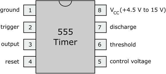
FIGURE 11-14: 555 timer IC pinout.
By connecting a few resistors, capacitors, and switches to the various pins of the 555 timer, you can get this little gem to perform loads of different functions — and it’s remarkably easy to do. You can find detailed, easy-to-read information about its various applications on datasheets. I discuss three popular ways to configure a timing circuit using a 555 here.
Astable multivibrator (oscillator)
The 555 can behave as an astable multivibrator, which is just a fancy term to describe a sort of electronic metronome. By connecting components to the chip (as shown in Figure 11-15), you configure the 555 to produce a continuous series of voltage pulses that automatically alternate between low (0 volts) and high (the positive supply voltage, VCC), as shown in Figure 11-16. (The term astable refers to the fact that this circuit does not settle down into a stable state, but keeps changing on its own between two different states.) This self-triggering circuit is also known as an oscillator.

FIGURE 11-15: A 555 astable multivibrator circuit configuration.
You can use the 555 astable multivibrator for lots of fun things:
- Flash lights: A low-frequency (<10 Hz) pulse train can control the on/off operation of an LED or lamp (see the LED flasher project in Chapter 17).
- Create an electronic metronome: Use a low-frequency (<20 Hz) pulse train as the input to a speaker or piezoelectric transducer to generate a periodic clicking sound.
- Sound an alarm: By setting the frequency to the audio range (20 Hz to 20 kHz) and feeding the output into a speaker or piezoelectric transducer, you can produce a loud, annoying tone (see the siren and light-sensing alarm projects in Chapter 17).
- Clock a logic chip: You can adjust the pulse widths to match the specifications for the signal that clocks the logic inside a chip, such as the 4017 decade counter I describe later in this chapter (see the light chaser and traffic light simulator projects in Chapter 17).
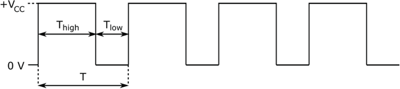
FIGURE 11-16: Series of voltage pulses from a 555 astable multivibrator circuit. External components control the pulse width.
The frequency f (in hertz), which is the number of complete up-and-down cycles per second, of the square wave produced is determined by your choice of three external components, according to this equation:
If you flip the numerator and dominator in that equation, you get the time period (T), which is the length of time (in seconds) of one complete up-and-down pulse:
You can set up your circuit so that the width of the high part of the pulse is different from the width of the low part of the pulse. To find the width of the high part of the pulse (expressed as Thigh), use the following equation:
You find the width of the low part of the pulse (expressed as Tlow) like this:
If R2 is much, much bigger than R1, the high and low pulse widths will be fairly equal. If R2=R1, the high portion of the pulse will be twice as wide as the low portion. You get the idea.
You can also use a potentiometer (variable resistor) in series with a small resistor as R1 or R2 and adjust its resistance to vary the pulses.
To choose values for R1, R2, and C1, I suggest you follow these steps:
- Choose C1. Decide what frequency range you want to generate and choose an appropriate capacitor. The lower the frequency range, the higher the capacitor you should choose. (Assume that R1 and R2 will be somewhere in the 10 kΩ to 1 MΩ range.) For many low-frequency applications, capacitor values of between 0.1 μF and 10 μF work well. For higher-frequency applications, choose a capacitor in the range of 0.01 μF to 0.001 μF.
- Choose R2. Decide how wide the low part of the pulse should be, and choose the value of R2 that will produce that width, given the value of C1 you’ve already determined.
- Choose R1. Decide how wide the high part of the pulse should be. Using the values of C1 and R2 already selected, calculate the value of R1 that will produce the desired high pulse width.
For instance, one way to produce a pulse that is high for about 3 seconds and low for about 1.5 seconds is to use a 10 μF capacitor for C1 and 220 kΩ resistors for both R1 and R2. (Plug those values into the equations for Thigh and Tlow and see for yourself!)
Monostable multivibrator (one-shot)
By configuring the 555 timer as shown in Figure 11-17, you can use it as a monostable multivibrator that generates a single pulse when triggered. This configuration is sometimes called a one-shot. Without a trigger, this circuit produces a low (zero) voltage; this is its stable state. When triggered by closing the switch between pin 2 and ground, this circuit generates an output pulse at the level of the supply voltage, VCC. The width of the pulse, T, is determined by the values of R1 and C1, as follows:
Because capacitor values can often vary by as much as 20%, you may need to choose a resistor with a different value than the formula suggests to produce the pulse width you desire.
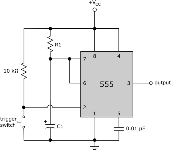
FIGURE 11-17: Triggered by closing the momentary switch at pin 2, the 555 monostable circuit produces a single pulse whose width is determined by the values of R1 and C1.
You can use a one-shot to safely trigger a digital logic device (such as the 4017 CMOS decade counter described later in this chapter). Mechanical switches tend to “bounce” when closed, producing multiple voltage spikes which a digital IC can misinterpret as multiple trigger signals. Instead, if you trigger a one-shot with a mechanical switch, and use the output of the one-shot to trigger the digital IC, you can effectively “de-bounce” the switch.
Bistable multivibrator (flip-flop)
If an astable circuit has no stable state and a monostable circuit has one stable state, what’s a bistable circuit? If you guessed that a bistable circuit is a circuit with two stable states, you are correct.
The 555 bistable multivibrator shown in Figure 11-18 produces alternating high (VCC) and low (0 V) voltages, switching from one state to the other only when triggered. Such a circuit is commonly known as a flip-flop. There’s no need to calculate resistor values; activating the trigger switch controls the timing of the pulses generated.

FIGURE 11-18: The 555 bistable circuit (or flip-flop) produces a high output when triggered by the switch at pin 2, and a low output when reset by the switch at pin 4.
You can witness firsthand how a 555 timer works as a flip-flop by building the circuit shown in Figure 11-19. Here are the parts you need:
- Four 1.5-volt AA batteries
- One four-battery holder (for AA batteries) with battery clip
- One 555 timer IC
- Two 10 kΩ resistors (brown-black-orange)
- One 470 Ω resistor (yellow-violet-brown)
- One LED (any size, any color)
- One single-pole, double-throw (SPDT) switch
- One solderless breadboard
- Assorted jumper wires
Set up the circuit, using Figure 11-20 as your guide. Note that one end of the SPDT switch is connected to pin 2 (trigger) of the 555 timer, the other end is connected to pin 4 (reset) of the 555 timer, and the center terminal is connected to ground. Depending on the position of the slider on the SPDT switch, the switch either triggers or resets the 555 timer.

FIGURE 11-19: Use an LED to visualize the output of a flip-flop circuit.
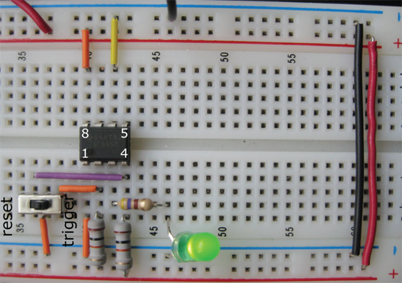
FIGURE 11-20: The SPDT switch is used to both trigger and reset the 555 timer in this flip-flop circuit. (Pin and switch labels have been added.)
After you set up the circuit, slide the switch to the trigger position. Does the LED light? Does it stay lit as long as you leave the switch in the trigger position? Now slide the switch to the reset position. Does the LED go off and stay off as long as the switch is in the reset position?
Because a flip-flop's output stays high (or low) until triggered (or reset), it can be used to store a data bit. (Remember, a bit is a 0 or a 1, which is a low voltage or a high voltage, respectively.) The registers used to store temporary outputs between stages of logic consist of multiple flip-flops. Flip-flops are also used in certain digital-counter circuits, holding bits in a series of interconnected registers that form an array, the outputs of which make up a bit string representing the count. (Refer to the sidebar, “Storing bits in registers,” earlier in this chapter, for more information on registers.)
You can use various types of 555 timer circuits to trigger other 555 timer circuits. For instance, you can use an oscillator to trigger a flip-flop (useful for clocking registers). Or you can use a one-shot to produce a temporary low-volume tone — and when it ends, change the state of a flip-flop, whose output triggers an oscillator that pulses a speaker on and off. Such a circuit might be used in a home alarm system: Upon entering the home, the homeowner (or intruder) has 10 seconds or so to deactivate the system (while hearing a low-volume warning tone) before the siren wakes up the neighbors.
Counting on the 4017 decade counter
The 4017 CMOS decade counter shown in Figure 11-21 is a 16-pin IC that counts from 0 to 9 when triggered. Pins 1–7 and 9–11 go from low to high one at a time when a trigger signal is applied to pin 14. (They don’t go from low to high in strict counterclockwise order; you have to check the pinout to determine the order.) You can use the count outputs to light LEDs (as in the light chaser and traffic light projects in Chapter 17) or trigger a one-shot that controls another circuit.

FIGURE 11-21: Pinout of the 4017 CMOS decade counter.
Counting can take place only when the disable pin (pin 13) is low; you can disable counting by applying a high signal to pin 13. You can also force the counter to reset to zero (meaning that the zero-count output, which is pin 3, goes high) by applying a high signal to pin 14.
By piggybacking multiple 4017 ICs, you can count up tens, hundreds, thousands, and so forth. Pin 12 is high when the count is 0 to 4 and low when the count is 5 to 9, so it looks like a trigger signal that changes from low to high at one-tenth the rate of the count. If you feed the output of pin 12 into the trigger input (pin 14) of another decade counter, that second counter will count up tens. By feeding the second counter’s pin-12 output into pin 14 of a third counter, you can count up hundreds. With enough 4017 ICs, you may even be able to tally the national debt!
You can also connect two or more of the counter’s outputs using diodes to produce a variable timing sequence. To do this, connect each anode (positive side of a diode) to an output pin, and connect all the cathodes (negative sides of the diodes) together and then through a resistor. With this arrangement, when any one of the outputs is high, current will flow through the resistor. For instance, you can simulate the operation of a traffic light by tying outputs 0–4 together and feeding the result (through a resistor) into a red LED, connecting output 5 to a yellow LED, and tying outputs 6–9 together to control a green LED. (See the traffic light project in Chapter 17.)
Microcontrollers
One of the most versatile integrated circuits you can find is the microcontroller. A microcontroller is a small, complete computer on a chip. To program it, you place it on a development board that allows the IC to interface with your personal computer. After it’s programmed, you mount the microcontroller into a socket on your electronic device (which could be a solderless breadboard). You add a few other components to provide an interface between the microcontroller and LEDs, motors, or switches — and voilà! Your little programmed IC makes things happen (for instance, it can control the motion of a robot). The nice thing about a microcontroller is that you can simply alter a few lines of code (or reprogram it completely) to change what it does; you don’t need to swap out wires, resistors, and other components to get this flexible IC to take on a new personality.
Hundreds of microcontrollers are available, but a handful are geared specifically for first-timers. Some, such as the one shown on the PCB in Figure 11-22, can be purchased as part of a complete development package: You get a pre-assembled printed circuit board populated with the microcontroller IC, discrete components, and standard connectors so that you can connect the microcontroller to a circuit during operation or to your computer for programming. Many of these kits also include an integrated development environment (IDE), which contains software tools for programming the microcontroller. (See Chapter 18 for more on microcontroller kits.)

FIGURE 11-22: The square chip that Mr. Washington is gazing at is a microcontroller that is surface-mounted to a mini PCB populated with additional components and a connector.
Other popular ICs
Among the other common functions provided by ICs are mathematical operations (addition, subtraction, multiplication, and division), multiplexing (selecting a single output from among several inputs), and the conversion of signals between analog and digital:
- You use an analog-to-digital (A/D) converter to convert a real-world analog signal into a digital signal so you can process it with a computer or other digital electronics system.
- You use a digital-to-analog (D/A) converter to convert a processed digital signal back into an analog signal. (For example, you need an analog signal to vibrate the speakers in your home computer system.)
Of course, the microprocessor that runs your personal computer (and maybe even your personal life) is also quite popular as ICs go.
There are so many more integrated circuits than I can possibly cover in this book. Really smart circuit designers are always coming up with new ideas and improvements on some old ideas, so there are a lot of choices in the world of integrated circuits.