
Chapter 3
Opamps and Their Properties
Introduction
Audio design has for many years relied on a very small number of opamp types; the TL072 and the 5532 dominated the audio small-signal scene for many years. The TL072, with its JFET inputs, was used wherever its negligible input bias currents and low cost were important. For a long time the 5534/5532 was much more expensive than the TL072, so the latter was used wherever feasible in an audio system, despite its inferior noise, distortion, and load-driving capabilities. The 5534 was reserved for critical parts of the circuitry. Although it took many years, the price of the 5534 is now down to the point where you need a very good reason to choose any other type of opamp for audio work.
The TL072 and the 5532 are dual opamps; the single equivalents are TL071 and 5534. Dual opamps are used almost universally, as the package containing two is usually cheaper than the package containing one, simply because it is more popular.
There are however other opamps, some of which can be useful, and a selected range is covered here.
Opamp Properties: Noise
There is no point in regurgitating manufacturer’s data sheets, especially since they are readily available on the internet. Here I have simply ranked the opamps most commonly used for audio in order of voltage noise (Table 3.1).
The great divide is between JFET input opamps and BJT input opamps. The JFET opamps have more voltage noise but less current noise than bipolar input opamps, the TL072 being particularly noisy. If you want the lowest voltage noise, it has to be a bipolar input. The difference however between a modern JFET input opamp such as the OPA2134 and the old faithful 5532 is only 4 dB; but the JFET part is a good deal more costly. The bipolar AD797 seems to be out on its own here, but it is a specialised and expensive part. The LT1028 is not suitable for audio use because its bias-current cancellation system makes it noisy in most circumstances. The LM741 has no noise specs on its data sheets, and the 20 nV/rtHz is from measurements.
Opamp |
### |
### |
Input device type |
Bias cancel? |
|---|---|---|---|---|
LM741 |
20 |
?? |
BJT |
No |
TL072 |
18 |
0.01 |
FET |
No |
OPA604 |
11 |
0.004 |
FET |
No |
NJM4556 |
8 |
Not spec’d |
BJT |
No |
OPA2134 |
8 |
0.003 |
FET |
No |
OP275 |
6 |
1.5 |
BJT+FET |
No |
OPA627 |
5.2 |
0.0025 |
FET |
No |
5532A |
5 |
0.7 |
BJT |
No |
LM833 |
4.5 |
0.7 |
BJT |
No |
MC33078 |
4.5 |
0.5 |
BJT |
No |
5534A |
3.5 |
0.4 |
BJT |
No |
OP270 |
3.2 |
0.6 |
BJT |
No |
OP27 |
3 |
0.4 |
BJT |
Yes |
LM4562 |
2.7 |
1.6 |
BJT |
No |
AD797 |
0.9 |
2 |
BJT |
No |
LT1028 |
0.85 |
1 |
BJT |
Yes |
Both voltage and current noise increase at 6 dB/octave below the 1/f corner frequency, which is usually around 100 Hz. The only way to minimise this effect is to choose an appropriate opamp type
Opamps with bias-cancellation circuitry are normally unsuitable for audio use due to the extra noise this creates. The amount depends on circuit impedances and is not taken into account in Table 3.1. The general noise behaviour of opamps in circuits is dealt with in Chapter 1.
Opamp Properties: Slew Rate
Slew rates vary more than most parameters; a range of 100:1 is shown here in Table 3.2. The slowest is the LM741, which is the only type not fast enough to give full output over the audio band. There are faster ways to handle a signal, such as current-feedback architectures, but they usually fall down on linearity. In any case, a maximum slew rate greatly in excess of what is required appears to confer no benefits whatever.
The 5532 slew rate is typically ±9 V/us. This version is internally compensated for unity-gain stability, not least because there are no spare pins for compensation when you put two opamps in an 8-pin dual package. The single-amp version, the 5534, can afford a couple of compensation pins, and so is made to be stable only for gains of 3x or more. The basic slew rate is therefore higher at ±13 V/us.
Compared with power amplifier specs, which often quote 100 V/us or more, these opamp speeds may appear rather sluggish. In fact they are not; even ±9 V/us is more than fast enough. Assume you are running your opamp from ±18V rails and that it can give a ±17V swing on its output. For most opamps this is distinctly optimistic, but never mind. To produce a full-amplitude 20 kHz sine wave you only need 2.1 V/us, so even in the worst case there is a safety margin of at least four times. Such signals do not of course occur in actual use, as opposed to testing. More information on slew-limiting is given in the section on opamp distortion.
Opamp |
V/us |
|---|---|
LM741 |
0.5 |
OP270 |
2.4 |
OP27 |
2.8 |
NJM4556 |
3 |
MC33078 |
7 |
LM833 |
7 |
5532A |
9 |
LT1028 |
11 |
TL072 |
13 |
5534A |
13 |
OPA2134 |
20 |
LM4562 |
20 |
AD797 |
20 |
OP275 |
22 |
OPA604 |
25 |
OPA627 |
55 |
Opamp Properties: Common-Mode Range
This is simply the range over which the inputs can be expected to work as proper differential inputs. It usually covers most of the range between the rail voltages, with one notable exception. The data sheet for the TL072 shows a common-mode (CM) range that looks a bit curtailed at −12V. This bland figure hides the deadly trap this IC contains for the unwary. Most opamps, when they hit their CM limits, simply show some sort of clipping. The TL072, however, when it hits its negative limit, promptly inverts its phase, so your circuit either latches up or shows nightmare clipping behaviour with the output bouncing between the two supply rails. The positive CM limit is in contrast trouble-free. This behaviour can be especially troublesome when TL072s are used in highpass Sallen and Key filters.
Opamp Properties: Input Offset Voltage
A perfect opamp would have its output at 0 V when the two inputs were exactly at the same voltage. Real opamps are not perfect, and a small voltage difference—usually a few millivolts—is required to zero the output. These voltages are large enough to cause switches to click and pots to rustle, and DC blocking is often required to keep them in their place.
The typical offset voltage for the 5532A is ±0.5 mV typical, ±4 mV maximum at 25 °C; the 5534A has the same typical spec but a lower maximum at ±2 mV. The input offset voltage of the new LM4562 is only ±0.1 mV typical, ±4 mV maximum at 25 °C.
Opamp Properties: Bias Current
Bipolar-input opamps not only have larger noise currents than their JFET equivalents, they also have much larger bias currents. These are the base currents taken by the input transistors. This current is much larger than the input offset current, which is the difference between the bias current for the two inputs. For example, the 5532A has a typical bias current of 200 nA, compared with a much smaller input offset current of 10 nA. The LM4562 has a lower bias current of 10 nA typical, 72 nA maximum. In the case of the 5532/4 the bias current flows into the input pins as the input transistors are NPN.
Bias currents are a considerable nuisance when they flow through variable resistors; they make them noisy when moved. They will also cause significant DC offsets when they flow through high-value resistors.
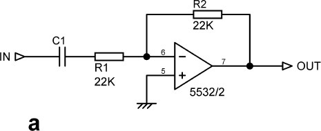
It is often recommended that the effect of bias currents can be cancelled out by making the resistance seen by each opamp input equal. Figure 3.1a shows a shunt- feedback stage with a 22 kΩ feedback resistor. When 200 nA flows through this it will generate a DC offset of 4.4 mV, which is rather more than we would expect from the input offset voltage error.
If an extra resistance, Rcompen, of the same value as the feedback resistor, is inserted into the noninverting input circuit then the offset will be cancelled. This strategy works well and is done almost automatically by many designers. However, there is a snag. The resistance Rcompen generates extra Johnson noise, and to prevent this it is necessary to shunt the resistance with a capacitor, as in Figure 3.1b. This extra component costs money and takes up PCB space, so it is questionable if this technique is actually very useful for audio work. It is usually more economical to allow offsets to accumulate in a chain of opamps and then remove the DC voltage with a single output blocking capacitor. This assumes that there are no stages with a large DC gain and that the offsets are not large enough to significantly reduce the available voltage swing. Care must also be taken if controls are involved, because even a small DC voltage across a potentiometer will cause it become crackly, especially as it wears.
FET-input opamps have very low bias current at room temperature; however it doubles for every 10 degree Centigrade rise. This is pretty unlikely to cause trouble in most audio applications, but a combination of high internal temperatures and high-value pots could lead to some unexpected crackling noises.
Opamp Properties: Cost
While it may not appear on the data sheet, the price of an opamp is obviously a major factor in deciding whether or not to use it. Table 3.3 was derived from the averaged prices for 1+ and 25+ quantities across a number of UK distributors. At the time of writing the cheapest popular opamps are the TL072 and the 5532, and these happened to come out at exactly the same price for 25+, so their price is taken as unity and used as the basis for the price ratios given.
Table 3.3 was compiled using prices for DIL packaging and the cheapest variant of each type. Price is per package and not per opamp section. It is obviously only a rough guide. Purchasing in large quantities or in different countries may change the rankings somewhat (even going from 1+ to 25+ causes some changes) but the basic look of things will not alter too much. One thing is obvious—the 5532 is one of the great opamp bargains of all time.
Price ratio |
Price ratio |
|||
|---|---|---|---|---|
Type |
Format |
1+ |
Type |
25+ |
LM833 |
Dual |
1.45 |
5532 |
1.00 |
5532 |
Dual |
1.64 |
TL072 |
1.00 |
MC33078 |
Dual |
1.97 |
LM833 |
1.12 |
TL072 |
Dual |
2.45 |
MC33078 |
1.27 |
OPA604 |
Single |
5.09 |
TL052 |
2.55 |
OPA2134PA |
Dual |
5.55 |
OP275GP |
3.42 |
TL052 |
Dual |
5.76 |
OPA2134PA |
4.45 |
OP275GP |
Dual |
7.18 |
OPA604 |
5.03 |
OP27 |
Single |
8.67 |
OP27 |
6.76 |
LM4562 |
Dual |
12.45 |
LM4562 |
9.06 |
AD797 |
Single |
25.73 |
AD797 |
13.09 |
OP270 |
Dual |
29.85 |
LT1028 |
17.88 |
LT1028 |
Single |
30.00 |
OPA270 |
24.42 |
OPA627 |
Single |
51.91 |
OPA627 |
48.42 |

Opamp Properties: Distortion
Relatively few discussions of opamp behaviour deal with nonlinear distortion, perhaps because it is a complex business. Opamp “accuracy” is closely related, but the term is often applied only to DC operation. Accuracy here is often specified in terms of bits, so “20-bit accuracy” means errors not exceeding one part in 2 to the 20, which is −120 dB or 0.0001%. Audio signal distortion is of course a dynamic phenomenon, very sensitive to frequency, and DC specs are of no use at all in estimating it.
Distortion is always expressed as a ratio and can be quoted as a percentage, as number of decibels, or in parts per million. With the rise of digital processing, treating distortion as the quantisation error arising from the use of a given number of bits has become more popular. Figure 3.2 hopefully provides a way of keeping perspective when dealing with these different metrics.
There are several different causes of distortion in opamps. We will now examine them.
Opamp Internal Distortion
This is what might be called the basic distortion produced by the opamp you have selected. Even if you scrupulously avoid clipping, slew-limiting, and common-mode issues, opamps are not distortion free, though some types such as the 5532 and the LM4562 have very low levels. If distortion appears when the opamp is run with shunt feedback, to prevent common-mode voltages on the inputs, and with very light output loading, then it is probably wholly internal and there is nothing to be done about it except pick a better opamp.
If the distortion is higher than expected, the cause may be internal instability provoked by putting a capacitative load directly on the output or neglecting the supply decoupling. The classic example of the latter effect is the 5532, which shows high distortion if there is not a capacitor across the supply rails close to the package; 100 nF is usually adequate. No actual HF oscillation is visible on the output with a general purpose oscilloscope, so the problem may be instability in one of the intermediate gain stages.

Slew Rate Limiting Distortion
While this is essentially an overload condition, it is wholly the designer’s responsibility. If users whack up the gain until the signal is within a hair of clipping, they should still be able to assume that slew-limiting will never occur, even with aggressive material full of high frequencies.
Arranging this is not too much of a problem. If the rails are set at the usual maximum voltage, i.e. ±18V, then the maximum possible signal amplitude is 12.7 Vrms, ignoring the saturation voltages of the output stage. To reproduce this level cleanly at 20 kHz requires a minimum slew rate of only 2.3 V/usec. Most opamps can do much better than this, though with the OP27 (2.8 V/usec) you are sailing rather close to the wind. The old LM741 looks as though it would be quite unusable, as its very limited 0.5 V/usec slew rate allows a full output swing only up to 4.4 kHz.
Horrific as it may now appear, audio paths full of LM741s were quite common in the early 1970s. Entire mixers were built with no other active devices, and what complaints there were tended to be about noise rather than distortion. The reason for this is that full-level signals at 20 kHz simply do not occur in reality; the energy at the HF end of the audio spectrum is well known to be much lower than that at the bass end.
This assumes that slew-limiting has an abrupt onset as level increases, rather like clipping. This is in general the case. As the input frequency rises and an opamp gets closer to slew-limiting, the input stage is working harder to supply the demands of the compensation capacitance. There is an absolute limit to the amount of current this stage can supply, and when you hit it the distortion shoots up, much as it does when you hit the supply rails and induce voltage clipping. Before you reach this point, the linearity may be degraded, but usually only slightly until you get close to the limit. It is not normally necessary to keep big margins of safety when dealing with slew-limiting. If you are employing the Usual Suspects in the audio opamp world—the TL072, the 5532, and the LM4562, with maximal slew rates of 13, 9, and 20 V/usec respectively—you are most unlikely to suffer any slew rate nonlinearity.
Distortion Due to Loading
Output stage distortion is always worse with heavy output loading because the increased currents flowing exacerbate the gain changes in the Class-B output stage. These output stages are not individually trimmed for optimal quiescent conditions (as are audio power amplifiers), and so the crossover distortion produced by opamps tends to be both higher and can be more variable between different specimens of the same chip. Distortion increases with loading in different ways for different opamps. It may rise only at the high-frequency end, (e.g. the OP2277), or there may be a general rise at all frequencies. Often both effects occur, as in the TL072.
The lowest load that a given opamp can be allowed to drive is an important design decision. It will typically be a compromise between the distortion performance required and opposing factors such as number of opamps in the circuit, cost of load-capable opamps, and so on. It even affects noise performance, for the lower the load resistance an amplifier can drive, the lower the resistance values in the negative feedback can be, and hence the lower the Johnson noise they generate. There are limits to what can be done in noise reduction by this method, because Johnson noise is proportional to the square root of circuit resistance and so improves only slowly as opamp loading is increased.
Thermal Distortion
Thermal distortion is that caused by cyclic variation of the properties of the amplifier components due to the periodic release of heat in the output stage. The result is a rapid rise in distortion at low frequencies, which gets worse as the loading becomes heavier.
Those who have read my work on audio power amplifiers will be aware that I am highly sceptical—in fact totally sceptical—about the existence of thermal distortion in amplifiers built from discrete components.[1] The power devices are too massive to experience per-cycle parameter variations, and there is no direct thermal path from the output stage to the input devices. There is no rise, rapid or otherwise, in distortion at low frequencies in a properly designed discrete power amplifier.
The situation is quite different in opamps, where the output transistors have much less thermal inertia and are also on the same substrate as the input devices. Nonetheless, opamps do not normally suffer from thermal distortion; there is generally no rise in low-frequency distortion, even with heavy output loading. Integrated- circuit power amplifiers are another matter, and the much greater amounts of heat liberated on the substrate do appear to cause serious thermal distortion, rising at 12 dB/octave below 50 Hz. I have never seen anything resembling this in any normal opamp.
Common-Mode Distortion
This is the general term for extra distortion that appears when there is a large signal voltage on both the opamp inputs. The voltage difference between these two inputs will be very small, assuming the opamp is in its linear region, but the common-mode (CM) voltage can be a large proportion of the available swing between the rails.
It appears to be by far the least understood mechanism, and gets little or no attention in opamp textbooks, but it is actually one of the most important influences on opamp distortion. It is simple to separate this effect from the basic forward-path distortion by comparing THD performance in series and shunt-feedback modes; this should be done at the same noise gain. The distortion is usually a good deal lower for the shunt-feedback case where there is no common-mode voltage. Bipolar and JFET input opamps show different behaviour, and they are treated separately. See Figure 3.3 for the various configurations examined.
Common-Mode Distortion: Bipolar Input Opamps
Figure 3.4 shows the distortion from a 5532 working in shunt mode with low-value resistors of 1 kΩ and 2k2 setting a gain of 2.2 times, at an output level of 5 Vrms. This is the circuit of Figure 3.3a with Rs set to zero; there is no CM voltage. The distortion is well below 0.0005% up to 20 kHz; this underlines what a superlative bargain the 5532 is.


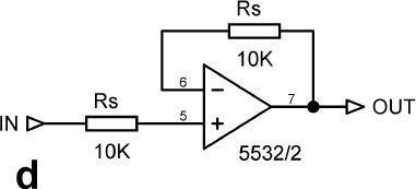

Figure 3.5 shows the same situation but with the output increased to 10 Vrms (the clipping level on ±18V rails is about 12 Vrms) and there is now significant distortion above 10 kHz, though it only exceeds 0.001% at 18 kHz.
This remains the case when Rs in Figure 3.3a is increased to 10 kΩ and 47 kΩ—the noise floor is higher, but there is no real change in the distortion behaviour. The significance of this will be seen in a moment.
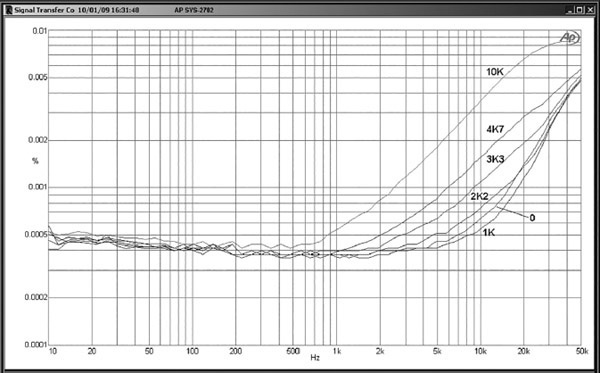
We will now connect the 5532 in the series-feedback configuration, as in Figure 3.3b; note that the stage gain is greater at 3.2 times but the opamp is working at the same noise gain. The CM voltage is 3.1 Vrms. With a 10 Vrms output we can see in Figure 3.6 that even with no added source resistance the distortion starts to rise from 2 kHz, though it does not exceed 0.001% until 12 kHz. But when we add some source resistance Rs, the picture is radically worse, with serious mid-band distortion rising at 6 dB/octave and roughly proportional to the amount of resistance added. We will note it is 0.0085% at 10 kHz with Rs = 47 kΩ.


The worst case for CM distortion is the voltage- follower configuration, as in Figure 3.3c, where the CM voltage is equal to the output voltage. Figure 3.7 shows that even with a CM voltage of 10 Vrms, the distortion is no greater than for the shunt mode. However, when source resistance is inserted in series with the input, the distortion mixture of second, third, and other low-order harmonics increases markedly. It increases with output level, approximately quadrupling as the level doubles. The THD is now 0.018% at 10 kHz with Rs = 47 kΩ, more than twice that of the series-feedback amplifier, due to the increased CM voltage.
It would be highly inconvenient to have to stick to the shunt-feedback mode because of the phase inversion and relatively low input impedance that comes with it, so we need to find out how much source resistance we can live with. Figure 3.8 zooms in on the situation with resistance of 10 kΩ and below; when the source resistance is below 2k2, the distortion is barely distinguishable from the zero source resistance trace. This is why the lowpass Sallen and Key filters in Chapter 13 have been given series resistors that do not in total exceed this figure.

Close examination reveals the intriguing fact that a 1 kΩ source actually gives less distortion than no source resistance at all, reducing THD from 0.00065% to 0.00055% at 10 kHz. Minor resistance variations around 1 kΩ make no difference. This must be due to the cancellation of distortion from two different mechanisms. It is hard to say whether it is repeatable enough to be exploited in practice; I wouldn’t want to rely on it.
So, what’s going on here? Is it simply due to nonlinear currents being drawn by the opamp inputs? Audio power amplifiers have discrete input stages which are very simple compared with those of most opamps and draw relatively large input currents. These currents show appreciable nonlinearity even when the output voltage of the amplifier is virtually distortion free, and if they flow through significant source resistances will introduce added distortion.[2]
If this was the case with the 5532 then the extra distortion would manifest itself whenever the opamp was fed from a significant source resistance, no matter what the circuit configuration. But we have just seen that it only occurs in series-feedback situations; increasing the source resistance in a shunt feedback does not perceptibly increase distortion. The effect may be present, but if so it is very small, no doubt because opamp signal input currents are also very small and it is lost in the noise.
The only difference is that the series circuit has a CM voltage of about 3 Vrms while the shunt circuit does not, and the conclusion is that with a bipolar input opamp, you must have both a CM voltage and a significant source resistance to see extra distortion. The input stage of a 5532 is a straightforward long-tailed pair with a simple tail current source and no fancy cascoding, and I suspect that Early effect operates on it when there is a large CM voltage, modulating the quite high input bias currents, and this is what causes the distortion. The signal input currents are much smaller, due to the high open-loop gain of the opamp, and as we have seen appear to have a negligible effect.
Common-mode Distortion: JFET Opamps
FET-input opamps behave differently from bipolar input opamps. Take a look at Figure 3.9, taken from a TL072 working in shunt and in series configuration with a 5 Vrms output. The circuits are as in Figure 3.3a, except that the resistor values have to be scaled up to 10 kΩ and 22 kΩ because the TL072 is nothing like so good at driving loads as the 5532. This unfortunately means that the inverting input is seeing a source resistance of 10k||22k = 6.9k, which introduces a lot of common-mode (CM) distortion—five times as much at 20 kHz as for the shunt case. Adding a similar resistance in the input path cancels out this distortion, and the trace then is the same as the “Shunt” trace in Figure 3.9. Disconcertingly, the value that achieved this was not 6.9k but 9.1k. That means adding −113 dBu of Johnson noise, so it’s not always appropriate.

It’s worth mentioning that the flat part of the shunt trace below 10 kHz is not noise, as it would be for the 5532; it is distortion.
A voltage-follower has no inconvenient medium- impedance feedback network, but it does have a much larger CM voltage. Figure 3.10 shows a voltage- follower working at 5 Vrms. With no source resistance the distortion is quite low, due to the 100% NFB, but as soon as a 10 kΩ source resistance is added we are looking at 0.015% at 10 kHz.
Once again, this can be cured by inserting an equal resistance in the feedback path of the voltage-follower, as in Figure 3.3d. This gives the “Cancel” trace in Figure 3.10. Adding resistances for distortion cancellation in this way has the obvious disadvantage that they introduce extra Johnson noise into the circuit. Another point is that stages of this kind are often driven from pot wipers, so the source impedance is variable, ranging between zero and one-quarter of the pot track resistance. Setting a balancing impedance in the other opamp input to a mid-value, i.e. one-eighth of the track resistance, should reduce the average amount of input distortion, but it is inevitably a compromise.
With JFET inputs the problem is not the operating currents of the input devices themselves, which are negligible, but the currents drawn by the nonlinear junction capacitances inherent in field-effect devices. These capacitances are effectively connected to one of the supply rails. For P-channel JFETs, as used in the input stages of most JFET opamps, the important capacitances are between the input JFETs and the substrate, which is normally connected to the V-rail. See Jung.[3]
According to the Burr-Brown data sheet for the OPA2134, “The P-channel JFETs in the input stage exhibit a varying input capacitance with applied CM voltage”. It goes on to recommend that the input impedances should be matched if they are above 2 kΩ.
Common-mode distortion can be minimised by running the opamp off the highest supply rails permitted, though the improvements are not large. In one test on a TL072, going from ±15V to ±18V rails reduced the distortion from 0.0045% to 0.0035% at 10 kHz.
Opamps Surveyed: BJT Input Types
The rest of this chapter looks at some opamp types and examines their performance, with the 5534A the usual basis for comparison. The parts shown here are not necessarily intended as audio opamps, though some, such as the OPA2134, were specifically designed as such. They have however all seen use, in varying numbers, in audio applications. Bipolar input opamps are dealt with first.

The NE5532/5534 Opamp
The 5532 is a low-noise, low-distortion bipolar dual opamp, with internal compensation for unity-gain stability. The 5534 is a single version internally compensated for gains down to three times, and an external compensation capacitor can be added for unity-gain stability; 22 pF is the usual value. The 5532 achieves unity-gain stability by having degeneration resistors in the emitter circuits of the input transistors, to reduce the open-loop gain, and this is why it is noisier than the 5534.
The common-mode range of the inputs is a healthy ±13V, with no nasty phase inversion problems if this is exceeded; there is more on the CM behaviour of the 5532/4 in the earlier section on common-mode distortion. It has a distinctly higher power consumption than the TL072, drawing approx. 4 mA per opamp section when quiescent. The DIL version runs perceptibly warm when quiescent on ±17 V rails.
The 5534/5532 has bipolar transistor input devices. This means it gives low noise with low source resistances but draws a relatively high bias current through the input pins. The input devices are NPN, so the bias currents flow into the chip from the positive rail. If an input is fed through a significant resistance, then the input pin will be more negative than ground due to the voltage drop caused by the bias current. The inputs are connected together with back-to-back diodes for reverse-voltage protection and should not be forcibly pulled to different voltages. The 5532 is intended for linear operation, and using it as a comparator is not recommended.
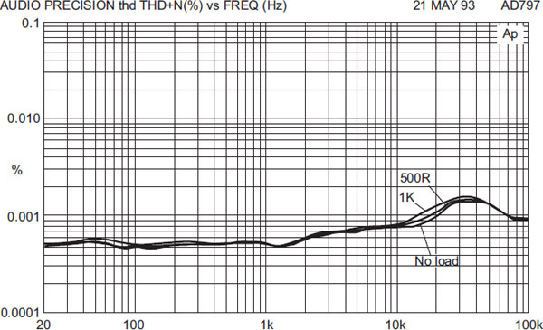
As can be seen from Figure 3.11, the 5532 has low distortion, even when driving the maximum 500 ohm load. The internal circuitry of the 5532 has never been officially explained but appears to consist of nested Miller loops that permit high levels of internal negative feedback. The 5532 is the dual of the 5534 and is much more commonly used than the single as it is cheaper per opamp and does not require an external compensation capacitor when used at unity gain.
The 5532/5534 is made by several companies, but they are not all created equal. Those by Fairchild, JRC, and ON-Semi have significantly lower THD at 20 kHz and above, and we’re talking about a factor of two or three here.
The 5532 and 5534 type opamps require adequate supply decoupling if they are to remain stable; otherwise they appear to be subject to some sort of internal oscillation that degrades linearity without being visible on a normal oscilloscope. The essential requirement is that the +ve and −ve rails should be decoupled with a 100 nF capacitor between them, at a distance of not more than a few millimetres from the opamp; normally one such capacitor is fitted per package as close to it as possible. It is not necessary, and often not desirable, to have two capacitors going to ground; every capacitor between a supply rail and ground carries the risk of injecting rail noise into the ground.
The 5534, and particularly the 5534A, have voltage and current noise parameters that are well suited to giving a good noise performance with MM cartridges. Using a standard cartridge with a series resistance of 610 Ω and a series inductance of 470 mH, (derived from the popular Shure M75ED Mk2), the calculated equivalent input noise is −122.5 dBu, so the output noise of a phono amplifier with +30 dB of gain (1 kHz) is −92.5 dBu. The effect of all circuit resistances is included with Rin = 47 kΩ and R0 = 220 Ω. Naturally this is with RIAA equalisation. A completely noiseless amplifier with all of the noise-generating resistances still present would have an EIN of −124.9 dBu with the same cartridge, which is only 2.4 dB better. This shows that using discrete devices instead of opamps can offer only small advantages. The subject of MM noise is dealt with in detail in Chapter 9.
Reducing 5532 Distortion by Output Stage Biasing
There is a useful, though relatively little-known (and where it is known, almost universally misunderstood and misapplied) technique for reducing the distortion of the 5532 opamp. While the method may be applicable to some other opamps, here I concentrate on the 5532, and it must not be assumed that the results will be emulated by any other opamp.
If a biasing current of the right polarity is injected into the opamp output, then the output stage distortion can be significantly reduced. This technique is sometimes called “output stage biasing”, though it must be understood that this is current biasing and that the DC voltage conditions are not significantly altered. Because of the high level of voltage feedback, the DC potential at the output is shifted by only a tenth of a millivolt or so.
You may have recognised that this scheme is very similar to the crossover displacement (Class XD) system I introduced for power amplifiers, which also injects an extra current, either steady or signal-modulated, into the amplifier output.[4] It is not however quite the same in operation. In power amplifiers the main aim of crossover displacement is to prevent the output stage from traversing the crossover region at low powers. In the 5532, at least, the crossover region is not easy to spot on the distortion residual, the general effect being of second- and third-harmonic distortion rather than spikes or edges; it appears that the 5532 output stage is more linear when it is pulling rather than pulling up, and the biasing current is compensating for this.
For the 5532, the current must be injected from the positive rail; currents from the negative rail make the distortion emphatically worse. This confirms that the output stage of the 5532 is in some way asymmetrical in operation, for if it was simply a question of suppressing crossover distortion by crossover displacement, a bias current of either polarity would be equally effective. The continued presence of the crossover region, albeit displaced, would mean that the voltage range of reduced distortion would be quite small and centred on 0 V. It is rather the case that there is a general reduction in distortion across the whole of the 5532 output range, which seems to indicate that the 5532 output stage is better at sinking current than sourcing it, and therefore injecting a positive current is effective at helping out.
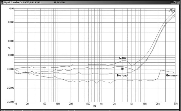
Figure 3.12a shows a 5532 running in shunt-feedback mode with a moderate output load of 1 kΩ; the use of shunt feedback makes it easier to see what’s going on by eliminating the possibility of common-mode distortion. With normal operation we get the upper trace in Figure 3.13, labelled “No bias”. If we then connect a current-injection resistor between the output and to the V+ rail, we find that the LF distortion (the flat bit) drops almost magically, giving the trace labelled “3K3”, which is only just above the gen-mon trace. Since noise makes a significant contribution to the THD residual at these levels, the actual reduction in distortion is greater than it appears.
The optimum resistor value for the conditions shown (5 Vrms and 1 kΩ load) is about 3k3, which injects a 5.4 mA current into the output pin. A 2k2 resistor gives greater distortion than 3k3, no doubt due to the extra loading it imposes on the output; in AC terms the injection resistor is effectively in parallel with the output load. In fact, 3k3 seems to be close to the optimal value for a wide range of output levels and output loadings.
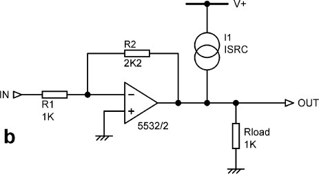
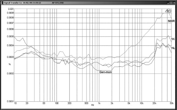
The extra loading that is put on the opamp output by the injection resistor is a disadvantage, limiting the improvement in distortion performance that can be obtained. By analogy with the canonical series of Class-A power amplifier outputs,[5] a more efficient and elegant way to inject the required biasing current is by using a current source connected to the V+ rail, as in Figure 3.12b. Since this has a very high output impedance the loading on the opamp output is not increased. Figure 3.12c shows practical way to do this; the current source is set to the same current that the 3k3 resistor injects when the output is at 0 V, (5.4 mA), but the improvement in distortion is greater. There is nothing magical about 5.4 mA; however, increasing the injection current to, say, 8 mA, gives only a small further improvement in the THD figure, and in some cases may make it worse; also the circuit dissipation is considerably increased, and in general I would not recommend using a current-source value of greater than 6 mA. Here in Table 3.4 are typical figures for a unity-gain shunt amplifier as before, with the loading increased to 680 Ω to underline that the loading is not critical; output biasing is effective with a wide range of loads.


As mentioned before, at such low THD levels the reading is largely noise, and the reduction of the distortion part of the residual is actually greater than it looks from the raw figures. Viewing the residual shows a dramatic difference.
You might be concerned about the Cbc of the transistor, which is directly connected to the opamp output. The 5532/5534 is actually pretty resistant to HF instability caused by load capacitance, and in the many versions of this configuration I tested I have had no problems whatever. The presence of the transistor does not reduce the opamp output swing.
Output biasing is also effective with series-feedback amplifier stages in some circumstances. Table 3.5 shows it working with a higher output level of 9.6 Vrms and a 1 kΩ load. The feedback resistors were 2k2 and 1 kΩ to keep the source resistance to the inverting input low.
Injection method |
THD at 1 kHz (22 kHz bandwidth) |
|---|---|
None |
0.00034% |
3k3 resistor |
0.00026% |
5.4 mA current source |
0.00023% |
8.1 mA current source |
0.00021% |
Injection method |
THD at 1 kHz (22 kHz bandwidth) |
|---|---|
None |
0.00037% |
3k3 resistor |
0.00033% |
5.4 mA current source |
0.00027% |
8.1 mA current source |
0.00022% |
The output biasing technique is in my experience only marginally useful with voltage followers, as the increased feedback factor with respect to a series amplifier with gain reduces the output distortion below the measurement threshold. Table 3.6 demonstrates this.
As a final example, Figure 3.14 shows that the output biasing technique is still effective with higher gains, here 14 times. The distortion with the 5.4 mA source is barely distinguishable from the testgear output up to 2 kHz. The series-feedback stage had its gain set by 1k3 and 100 Ω feedback resistors, their values being kept low to minimise common-mode distortion. It also underlines the point that in some circumstances an 8.1 mA current source gives worse results than the 5.4 mA version.
When extra common-mode distortion is introduced by the presence of a significant source resistance, this extra distortion is likely to swamp the improvement due to output biasing. In a 5532 amplifier stage with a gain of 3.2 times and a substantial source resistance, the basic output distortion with a 1 kΩ load at 9.6 Vrms, 1 kHz out was 0.0064%. A 3k3 output biasing resistor to V+ reduced this to 0.0062%, a marginal improvement at best, and an 8.1 mA current source could only reduce it to 0.0059%.
Earlier I said that the practice of output stage biasing appears to be pretty much universally misunderstood, judging by how it is discussed on the Internet. The evidence is that every application of it that my research has exposed shows a resistor (or current source) connected between the opamp output and the negative supply rail. This seems to be based on the assumption that displacing the crossover region in either direction is a good idea, coupled with a vague feeling that a resistor to the negative rail is somehow more “natural”, though how that conclusion was reached I cannot guess. However, the assumption that the output stage is symmetrical is usually incorrect; as we have seen, it is certainly not true for the 5532/5534. For the 5532—which surely must be the most popular audio opamp by a long way—a pulldown resistor would be completely inappropriate, as it increases rather than decreases the output stage distortion.
Injection method |
THD at 1 kHz (22 kHz bandwidth) |
|---|---|
None |
0.00018% (almost all noise) |
3k3 resistor |
0.00015% (all noise) |
5.4 mA current source |
0.00015% (all noise) |
8.1 mA current source |
0.00015% (all noise) |

You may be thinking that this is an ingenious method of reducing distortion, but rather clumsy compared with simply using a more linear opamp like the LM4562. This is true, but on the other hand, if the improvement from output biasing is adequate, it will be much cheaper than switching to a more advanced opamp that costs ten times as much.
The LM4562 Opamp
The LM4562 is a new opamp, which first become freely available at the beginning of 2007. It is a National Semiconductor product. It is a dual opamp—there is no single or quad version. It costs about ten times as much as a 5532.
The input noise voltage is typically 2.7 nV/√Hz, which is substantially lower than the 4 nV/√Hz of the 5532. For suitable applications with low source impedances this translates into a useful noise advantage of 3.4 dB. However, with MM cartridges the greater current noise means that the overall noise is higher than that of the 5532 or 5534.
The bias current is 10 nA typical, which is very low and would normally imply that bias cancellation, with its attendant noise problems, was being used. However in my testing I have seen no sign of excess noise, and the data sheet is silent on the subject. No details of the internal circuitry have been released so far, and quite probably never will be.
It is not fussy about decoupling, and as with the 5532, 100 nF across the supply rails close to the package should ensure HF stability. The slew rate is typically ±20 V/us, more than twice as quick as the 5532.
The first THD plot in Figure 3.15 shows the LM4562 working at a closed-loop gain of 2.2x in shunt-feedback mode, at a high level of 10 Vrms. The top of the THD scale is 0.001%, something you will see with no other opamp in this survey. The no-load trace is barely distinguishable from the AP SYS-2702 output, and even with a heavy 500 Ω load driven at 10 Vrms there is only a very small amount of extra THD, reaching 0.0007% at 20 kHz.
Figure 3.16 shows the LM4562 working at a gain of 3.2x in series-feedback mode, both modes having a noise gain of 3.2x. There is little extra distortion from 500 Ω.
For Figures 3.15 and 3.16 the feedback resistances were 2k2 and 1 kΩ, so the minimum source resistance presented to the inverting input is 687 Ω. In Figure 3.17 extra source resistances were then put in series with the input path, (as was done with the 5532 in the earlier section on common-mode distortion), and this revealed a remarkable property of the LM4562—it is much more resistant to common-mode distortion than the 5532. At 10 Vrms and 10 kHz, with a 10 kΩ source resistance, the 5532 generates 0.0014% THD (see Figure 3.6), but the LM4562 gives only 0.00046% under the same conditions. I strongly suspect that the LM4562 has a more sophisticated input stage than the 5532, probably incorporating cascoding to minimise the effects of common-mode voltages.

Note that only the rising curves to the right represent actual distortion. The raised levels of the horizontal traces at the LF end are due to Johnson noise from the extra series resistance.
It has taken an unbelievably long time—nearly thirty years—for a better audio opamp than the 5532 to come along, but at last it has happened. At present it also has a much higher price, but hopefully that will change. The LM4562 is superior in just about every parameter, except for its higher current noise. This leads to an EIN with the standard cartridge of −117.9 dB, a significant 4.6 dB noisier than the humble 5534A.

The AD797 Opamp
The AD797 (Analog Devices) is a single opamp with very low voltage noise and distortion. It appears to have been developed primarily for the cost-no-object application of submarine sonar, but it works very effectively with normal audio—if you can afford to use it. The cost is something like twenty times that of a 5532. No dual version is available, so the cost ratio per opamp section is forty times.
Early versions appeared to be rather difficult to stabilise at HF, but the current product is no harder to apply than the 5532. Possibly there has been a design tweak, or on the other hand my impression may be wholly mistaken.
The AD797 incorporates an ingenious feature for internal distortion cancellation. This is described on the manufacturer’s data sheet. Figure 3.18 shows that it works effectively.
This is a remarkably quiet device in terms of voltage noise, but current noise is correspondingly high due to the high collector currents in the input devices, and so it is noisy when used with an MM cartridge. The EIN is −116.6 dBu, a big 6.0 dB worse than the 5534A and a poor return for an expensive part. It has however been used for MC inputs, for which it is more suitable.
The OP27 Opamp
The OP27 from Analog Devices is a bipolar input single opamp primarily designed for low noise and DC precision. It was not intended for audio use, but in spite of this it is frequently recommended for applications as RIAA phono amplifiers. This is most unfortunate, because while at first sight it appears that the OP27 is quieter than the 5534/5532, as the en is 3.2 nV/rtHz compared with 4 nV/rtHz for the 5534, in practice it is usually slightly noisier. This is because the OP27 is in fact optimised for DC characteristics and so has input bias-current cancellation circuitry that generates common-mode noise. When the impedances on the two inputs are very different—which is the case in RIAA preamps—the CM noise does not cancel, and this appears to degrade the overall noise performance significantly. This opamp may be useful in other parts of the circuitry, but is not recommended for MM input amplifiers.
For a bipolar input opamp, there appears to be a high level of common-mode input distortion, enough to bury the output distortion caused by loading; see Figures 3.19 and 3.20. It is likely that this too is related to the bias- cancellation circuitry, as it does not occur in the 5532.
The maximum slew rate is low compared with other opamps, being typically 2.8V/us. However, this is not the problem it may appear. This slew rate would allow a maximum amplitude at 20 kHz of 16 Vrms, if the supply rails permitted it. I have never encountered any particular difficulties with decoupling or stability of the OP27.
Because the effects on noise of the input bias-current cancellation circuitry depend very much on external circuit resistances, it is not possible to compare the OP27 with other opamps directly. However my experience is that there is at least a 2 dB noise penalty compared with the 5534A.
Opamps Surveyed: JFET Input Types
Opamps with JFET inputs tend to have higher voltage noise and lower current noise than BJT input types and are therefore give a better noise performance with high source resistances. Their very low bias currents often allow circuitry to be simplified.


The TL072 Opamp
The TL072 is one of the most popular opamps, having very high-impedance inputs with effectively zero bias and offset currents. The JFET input devices give their best noise performance at medium impedances, in the range 1 kΩ–10 kΩ. It has a modest power consumption, at typically 1.4 mA per opamp section, which is significantly less than the 5532. The slew rate is higher than for the 5532, at 13 V/us against 9 V/us. The TL072 is a dual opamp. There is a single version called the TL071 which has offset null pins.
However, the TL072 is not THD-free in the way the 5532 is. In audio usage, distortion depends primarily upon how heavily the output is loaded. The maximum loading is a trade-off between quality and circuit economy, and I would put 2 kΩ as the lower limit. This opamp is not the first choice for audio use unless the near-zero bias currents (which allow circuit economies by making blocking capacitors unnecessary), the low price, or the modest power consumption are dominant factors.
It is an unhappy quirk of this device that the input common-mode range does not extend all the way between the rails. If the common-mode voltage gets to within a couple of volts of the V-rail, the opamp suffers phase reversal and the inputs swap their polarities. There may be really horrible clipping, where the output hits the bottom rail and then shoots up to hit the top one, or the stage may simply latch up until the power is turned off. There is more on the CM behaviour of the TL072 in the earlier section on common-mode distortion.
TL072s are relatively relaxed about supply rail decoupling, though they will sometimes show very visible oscillation if they are at the end of long, thin supply tracks. One or two rail-to-rail decoupling capacitors (e.g. 100 nF) per few centimetres is usually sufficient to deal with this, but the usual practice is to not take chances and allow one capacitor per package, as with other opamps.
Because of common-mode distortion, a TL072 in shunt configuration is always more linear. In particular compare the results for a 3k3 load in Figures 3.21 and 3.22. At heavier loadings the difference is barely visible because most of the distortion is coming from the output stage.
Distortion always gets worse as the loading increases. This factor together with the closed-loop NFB factor determines the THD.
TL072/71 opamps are prone to HF oscillation if faced with significant capacitance to ground on the output pin; this is particularly likely when they are used as unity-gain buffers with 100% feedback. A few inches of track can sometimes be enough. This can be cured by an isolating resistor, in the 47–75 Ω range, in series with the output, placed at the opamp end of the track.


The TL072 has low current noise, because of its JFET inputs, but the voltage noise is high at 18nV/√Hz, leading to an EIN with the standard cartridge of −113.4 dBu, 9.1 dB worse than the 5534A. It is the worst noise result so far.
The OPA2134 Opamp
The OPA2134 is a Burr-Brown product, the dual version of the OPA134. The manufacturer claims it has superior sound quality due to its JFET input stage. Regrettably, but not surprisingly, no evidence is given to back up this assertion. The slew rate is typically ±20 V/us, which is ample. It does not appear to be optimised for DC precision, the typical offset voltage being ±1 mV, but this is usually good enough for audio work. I have used it many times as a DC servo in power amplifiers, the low bias currents allowing high resistor values and correspondingly small capacitors.
The OPA2134 does not show phase reversal anywhere in the common-mode range, which immediately marks it as superior to the TL072.
The two THD plots in Figures 3.23 and 3.24 show the device working at a gain of 3x in both shunt and series-feedback modes. It is obvious that a problem emerges in the series plot, where the THD is higher by about three times at 5 Vrms and 10 kHz. This distortion increases with level, which immediately suggests common-mode distortion in the input stage. Distortion increases with even moderate loading; see Figure 3.25.
This is a relatively modern and sophisticated opamp. When you need JFET inputs (usually because significant input bias currents would be a problem), this definitely beats the TL072; it is however four to five times more expensive.
The input noise voltage is 8 nV/√Hz, more than twice that of the 5532, and despite the low current noise this leads to an EIN of −116.6 dBu with the standard cartridge; this is 5.9 dB noisier than the 5534A.
Other Opamps
This chapter has only space to cover the opamps most likely to be useful in electronics for vinyl. Other opamps are examined in Small Signal Audio Design;[5] the LM741, OP270, and OP275 with BJT input devices, and the TL052, OPA604, and OP627 with JFET input devices. Opamps for operation from a +5V rail are also analysed. None of these devices have performance that exceeds the opamps described in this chapter; their noise performance can however be found in Chapter 9 of this book.


Selecting the Right Opamp
Until recently, the 5532/4 was pre-eminent in almost all audio electronics. It is found in almost every mixing console and in a large number of preamplifiers. Distortion is almost very low, even when driving 600 Ω loads. Noise is very low, and the balance of voltage and current noise in the input stage is well-matched to moving-magnet phono cartridges; using exotic discrete devices cannot give more than a dB or two advantage. Large-quantity production has brought the price down to a point where a powerful reason is required to pick any other device. The lowest noise version, and the best noise match to an MM cartridge, is the 5534A, but this comes in a single package and so costs more per opamp.
The 5532 is not, however, perfect. It suffers common-mode distortion. It has high bias and offset currents at the inputs as an inevitable result of using a bipolar input stage (for low noise) without any sort of bias- cancellation circuitry. The 5532 is not in the forefront for DC accuracy, though it’s not actually that bad. The offset voltage spec is 0.5 mV typical, 4 mV max, compared with 3 mV typical, 6 mV max for the popular TL072. I have actually used 5532s to replace TL072s when offset voltage was a problem, but the increased bias current was acceptable.
With horrible inevitability, the very popularity and excellent technical performance of the 5532 has led to it being criticised by Subjectivists who have contrived to convince themselves that they can tell opamps apart by listening to music played through them. This always makes me laugh like a drain, because there is probably no music on the planet that has not passed through a hundred or more 5532s on its way to the consumer.
There are two distinct roles for opamps in phono amplifiers. The critical first stage driven by an MM cartridge requires not only low voltage noise but also low current noise for the lowest noise output, and the 5534A wins this handily. It is the first choice, though the 5532 is not far behind and saves money because of its dual package.
The other role is in what might be called general purpose signal processing; subsonic and ultrasonic filters, flat gain stages, and so on. Here the LM4562, with its lower voltage noise and very low distortion, represents a real advance on the 5532/4. It is however still a good deal more expensive, and is not perfect—it appears to be more easily damaged by excess common-mode voltages, and there is some evidence it is more susceptible to RF demodulation when used as a voltage-follower.
References
1. Self, D. Audio Power Amplifier Design. 6th edition, Focal Press, 2013, p. 120. ISBN 978-0-240-52613-3, 978-0-240-52614-0.
2. Self, D. Audio Power Amplifier Design. 6th edition, Focal Press, 2013, p. 119.
3. Jung, W. ed. Op-amp Applications Handbook. Newnes, 2006, Chapter 5, p. 399.
4. Audio Power Amplifier Design, 6th edition, chapter 18.
5. Audio Power Amplifier Design, 6th edition, p. 425.
6. Self, D. Small Signal Audio Design. 2nd edition. Focal Press, 2015, Chapter 4. ISBN: 978-0-415-70974-3 (hbk) ISBN: 978-0-415-70973-6 (pbk) ISBN: 978-1-315-88537-7 (ebk).